RF PCB

Build Reliable RF PCBs for High-Frequency Applications

Controlled impedance, stable materials, precision fabrication, and engineering support—from rapid prototypes to production.

  • 1 Stable Material Supply for Faster RF PCB Production
  • 2 Advanced Manufacturing for Complex RF PCB Designs
  • 3 RF Engineering & DFM Support to Reduce Manufacturing Risk
  • 4 Rapid Prototyping with a Clear Path to Production

Why PCBMASTER

Why Choose PCBMASTER for RF PCB Manufacturing?

Choosing the right RF PCB manufacturer is critical to maintaining signal integrity, impedance consistency, and stable high-frequency performance. PCBMASTER focuses on the specific manufacturing requirements of RF PCB, from material selection and stack-up design to precision fabrication and quality control.

With experience in high-frequency PCB manufacturing, PCBMASTER supports RF PCB requirements such as controlled impedance, low-loss materials, precise trace geometry, stable dielectric thickness, and reliable multilayer structures. Our engineering team can review your RF PCB design and manufacturing requirements before production to identify potential issues early.

PCBMASTER also provides stable material sourcing for high-frequency laminates and other RF PCB materials, helping reduce material-related delays during prototyping and production. Whether you need an RF PCB prototype or volume manufacturing, you can work with the same manufacturing partner as your project develops.

Supported by ISO 9001, IATF 16949, UL certification, and RoHS compliance, PCBMASTER applies controlled quality processes throughout RF PCB manufacturing. From RF PCB material selection to fabrication and testing, PCBMASTER helps you build reliable RF PCBs with consistent performance and production quality.

Manufacturing Capabilities

Inside Our PCB Manufacturing Facilities

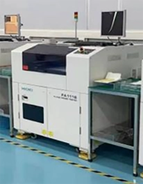
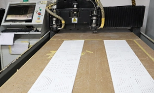
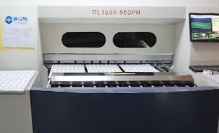
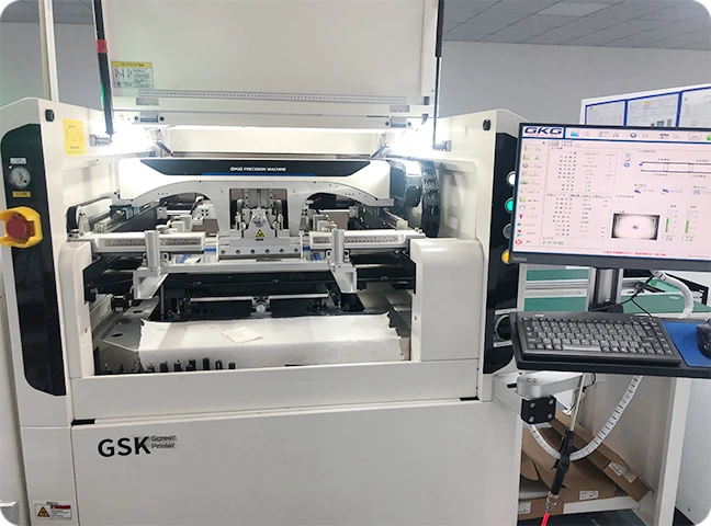
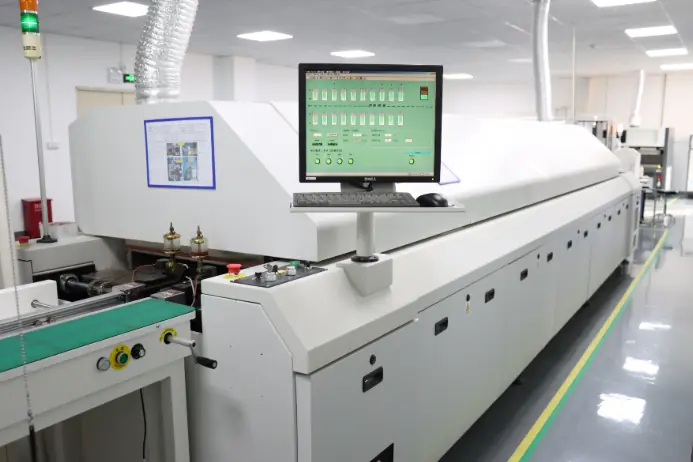
Our production lines cover the full PCB manufacturing process—from inner-layer imaging and lamination to drilling, plating, surface finish, and final inspection. These facilities support the technical requirements behind RF PCB manufacturing, including controlled-impedance routing, low-loss material handling, and precision multilayer registration.

PCB manufacturing facility 1
PCB manufacturing facility 2
PCB manufacturing facility 3
PCB manufacturing facility 4
PCB manufacturing facility 5
PCB manufacturing facility 6
PCB manufacturing facility 7
PCB manufacturing facility 8

Product Introduction

What Is an RF PCB?

An RF PCB (Radio Frequency Printed Circuit Board) is designed to transmit and process RF signals where high-frequency electrical behavior becomes critical. An RF PCB must carefully control transmission lines, ground planes, dielectric properties, trace geometry, and impedance to maintain signal integrity and minimize signal loss and reflection.

Compared with a standard PCB, an RF PCB places greater emphasis on high-frequency performance. Standard PCBs commonly use FR-4 with general dielectric and impedance requirements, while RF PCBs may require specialized high-frequency materials, tighter dielectric control, RF-specific stack-ups, controlled impedance, and carefully defined trace geometry.

PCBMASTER supports your RF PCB manufacturing through an integrated workflow: Design → Material → Stack-up → Fabrication → Impedance → Testing → Assembly. From RF PCB material selection and engineering review to precision fabrication and quality testing, this process helps reduce manufacturing risks and provides a reliable path from RF PCB prototype to production.

Key Features

RF PCB Features Designed for Stable RF Performance

Your RF PCB is built around the electrical and physical requirements of high-frequency signal transmission. Its material, impedance, transmission-line structure, grounding, and stack-up directly influence signal quality, loss, and overall RF performance.

Feature Description
Maintain Stable High-Frequency Signal Transmission RF PCB construction is optimized for high-frequency signals, helping you maintain more predictable signal behavior across demanding RF applications.
Achieve Consistent Impedance Controlled impedance helps you reduce signal reflections and maintain more predictable RF signal transmission.
Reduce High-Frequency Signal Loss Low-loss dielectric materials can reduce signal attenuation, helping you preserve signal strength as frequency increases.
Maintain Predictable RF Performance Stable dielectric properties provide more consistent electrical behavior, helping you achieve predictable RF performance across your operating frequency range.
Improve Transmission-Line Performance Precisely defined RF traces help you maintain the required electrical characteristics and support consistent high-frequency signal transmission.
Provide a More Reliable Signal Return Path Dedicated ground structures help provide controlled return paths, reducing unwanted coupling and supporting better signal integrity.
Support Controlled RF Signal Routing An RF-optimized stack-up helps you maintain appropriate relationships between signal, ground, and dielectric layers for high-frequency circuits.
Reduce Parasitic Effects Compact RF interconnect structures help minimize unwanted parasitic capacitance and inductance, supporting more predictable RF behavior.

Product Categories

Explore Our RF PCB Solutions

PCBMASTER provides a range of RF PCB types to meet different circuit structures, signal requirements, space constraints, and RF application needs. From simple RF circuits to complex high-frequency systems, you can choose the RF PCB structure that best fits your project.

Product Description
Single-Sided RF PCB A practical RF PCB solution for relatively simple circuits with straightforward routing and lower layout complexity.
Double-Sided RF PCB Provides additional routing and grounding space for RF circuits with moderate complexity and component density.
Multilayer RF PCB Separates RF signals, ground, power, and digital circuits to support more complex high-frequency system designs.
High-Frequency RF PCB Uses suitable high-frequency materials and structures for applications requiring controlled dielectric properties and reduced signal loss.
High-Speed RF PCB Designed for systems where RF circuits operate alongside high-speed digital signals and require controlled signal integrity.
RF HDI PCB Uses high-density interconnect technologies such as microvias to support compact RF layouts and fine-pitch components.
RF Rigid-Flex PCB Combines rigid and flexible sections to provide space-saving routing and reliable interconnections for compact RF devices.
RF Flexible PCB Offers lightweight and bendable circuit structures for RF modules, antennas, and applications with limited installation space.
RF Antenna PCB Integrates PCB antenna structures for wireless communication, RF transmission, and compact antenna applications.

Applications

RF PCB Applications

RF PCB is used across communication, automotive, IoT, aerospace, and test equipment to route, transmit, receive, and process high-frequency signals. Its specific role varies according to the electrical and structural requirements of each application.

Application How RF PCB Works in the Application
5G & Wireless Communication Routes high-frequency signals between antennas, transceivers, filters, and amplifiers, helping maintain controlled impedance and signal integrity.
RF Modules Integrates antennas, filters, amplifiers, mixers, and other RF components into compact circuits for signal transmission and processing.
Radar Systems Carries transmit and receive signals between RF circuits and antennas, supporting stable signal generation, reception, and processing.
Automotive Radar Connects radar transceivers with antenna elements, enabling high-frequency signal transmission for object detection and distance measurement.
IoT Devices Enables wireless transceivers and antennas to communicate through compact, controlled signal paths for reliable wireless transmission and reception.
Satellite Communication Links antennas, amplifiers, filters, and transceivers to support high-frequency signal transmission and reception in communication systems.
Wireless Infrastructure Supports RF transceiver, filtering, amplification, and antenna circuits in base stations and wireless equipment for high-frequency signal processing.
Test & Measurement Provides controlled signal paths between RF sources, connectors, filters, and measurement circuits for high-frequency signal generation and analysis.

Technical Parameters

RF PCB Specifications You Need to Define Before Quoting

Before requesting an RF PCB quote, providing the right technical specifications helps ensure accurate material selection, manufacturing evaluation, pricing, and lead-time estimation.

Parameter What It Means How to Define It for Your RF PCB
Frequency The operating frequency of your RF circuit. Provide the target frequency or frequency range to determine suitable materials and construction.
Dk Describes how the PCB material affects RF signal propagation. Specify the required Dk if defined by your design or application.
Df Indicates dielectric loss in the PCB material. Consider lower-loss materials when signal attenuation is a major concern.
Impedance The electrical characteristic of the RF transmission line. Provide your required impedance, such as 50 Ω, when specified by the design.
Layer Count Determines the arrangement of signal, ground, and power layers. Define it according to routing density, grounding, and circuit complexity.
Board Thickness The overall thickness of the finished RF PCB. Specify based on mechanical, enclosure, and stack-up requirements.
Copper Thickness The thickness of conductive copper layers. Define according to circuit, trace, thermal, and manufacturing requirements.
Trace Width The width of RF transmission lines. Define according to your impedance and stack-up requirements.
Trace Spacing The distance between conductive features. Set according to RF isolation and coupling requirements.
Surface Finish The protective finish applied to exposed copper. Select according to RF, assembly, and reliability requirements.
Via Structure Defines connections between different PCB layers. Specify via structures according to RF routing and grounding needs.
Material The laminate system used for the RF PCB. Select based on frequency, Dk, Df, loss, thermal requirements, and budget.
Tolerance The permitted variation in manufacturing dimensions. Define tighter tolerances where RF performance is particularly sensitive.

Not sure which specifications your RF PCB requires? Send PCBMASTER your Gerber files, stack-up, or basic electrical requirements, and our engineering team can review the available information for your RF PCB quotation.

Ready to Build Your RF PCB?

Upload your RF PCB files and requirements. Get engineering support for material selection, stack-up, controlled impedance, and manufacturing—then move confidently from prototype to production.

Material Options

Choose the Right Material for Your RF PCB

PCBMASTER provides multiple RF PCB material options to match your operating frequency, signal-loss requirements, thermal conditions, and application environment.

RF PCB Material Key Characteristics Typical Application
FR-4 RF PCB Cost-effective and suitable for RF designs with moderate frequency and less demanding loss requirements. General RF circuits, wireless devices
PTFE RF PCB Low-loss dielectric characteristics make it suitable for demanding high-frequency and microwave signal transmission. RF, microwave, antenna circuits
Rogers RF PCB Offers specialized high-frequency laminate systems with controlled dielectric and loss characteristics. 5G, radar, RF modules, high-frequency communication
Ceramic RF PCB Combines high-frequency performance with strong thermal and dimensional stability for demanding environments. High-frequency, high-temperature, high-reliability applications
Hybrid RF PCB Combines RF materials with FR-4 in different layers to balance RF performance, manufacturability, and cost. RF + digital mixed systems

Material selection directly affects RF PCB signal loss, impedance control, thermal performance, and transmission stability. For your project, PCBMASTER can help evaluate the required material based on frequency, circuit structure, electrical specifications, and application conditions.

Quality Assurance

Quality Assurance for Your RF PCB

PCBMASTER applies controlled quality processes throughout RF PCB manufacturing, supported by internationally recognized quality and compliance standards.

ISO 9001
IATF 16949
UL Certification
RoHS

Case Studies

RF PCB Case Studies: From Design Challenges to Production

Explore how PCBMASTER addresses different RF PCB requirements through practical projects, from material and stack-up selection to impedance control and precision manufacturing.

01

5G RF Module

28 GHz12 LayersLow-Loss RF Laminate50 Ω

The customer was developing a 28 GHz 5G RF module and needed a 12-layer RF PCB measuring approximately 120 × 80 mm. The design required low-loss laminate and 50 Ω controlled-impedance RF lines, while RF, power, and high-speed digital signals had to fit within a compact stack-up. Maintaining consistent impedance was the main challenge.

PCBMASTER reviewed the material, stack-up, dielectric thickness, trace geometry, and grounding structure before fabrication. The engineering team also used impedance test coupons to verify critical manufacturing parameters.

The prototype was completed for engineering validation, and the finalized construction was retained for subsequent production.

02

Automotive Radar PCB

77 GHz4 LayersPTFE-Based RF Laminate50 Ω

The project involved a 77 GHz automotive radar module for an ADAS application. The customer required a compact 4-layer RF PCB using a low-loss PTFE-based laminate, with 50 Ω transmission lines and a dedicated antenna area. At this frequency, small variations in dielectric thickness and trace geometry could affect RF performance.

PCBMASTER evaluated the material construction and stack-up, then optimized the critical RF geometries and controlled fabrication tolerances around the antenna and transmission-line areas.

The prototype passed the customer's initial PCB-level validation and was prepared for the next NPI stage.

03

Wireless Communication PCB

8 Layers100 × 70 mmControlled ImpedanceWireless Communication

The customer needed an 8-layer RF PCB for wireless communication equipment, combining RF transceiver circuits, power management, and digital control on a 100 × 70 mm board. Multiple controlled-impedance paths had to coexist with high-speed digital routing without excessive coupling.

PCBMASTER reviewed the layer arrangement and grounding strategy, separating sensitive RF paths from high-speed digital sections and establishing appropriate reference planes.

The finished RF PCB supported prototype assembly and functional verification, while the same construction could be carried into subsequent production.

04

RF Test Equipment PCB

6 Layers50 ΩRF Connectors, Filters & AttenuatorsRF Signal Measurement

For an RF test equipment project, the customer required a 6-layer PCB for a high-frequency signal-generation and measurement module. The board included RF connectors, filters, attenuators, and measurement circuits with 50 Ω controlled-impedance paths. Connector transitions and via structures were particularly sensitive.

PCBMASTER reviewed the RF stack-up and routing, controlled critical trace dimensions, and incorporated impedance test structures into the production panel.

The prototype was used for equipment-level validation and subsequent design optimization.

Customer Reviews

What Customers Say About Our RF PCB Manufacturing

See what customers value most when working with PCBMASTER on demanding RF PCB projects—from consistent quality and engineering support to fast prototyping and complex manufacturing.

RF PCB Quality
I don't judge an RF PCB supplier by the first batch alone. What matters to me is whether the board construction stays consistent when we build it again. With PCBMASTER, we paid close attention to impedance, dielectric thickness, and critical trace geometry. The consistency of the RF PCBs gave us much more confidence during our RF validation, and we didn't have to spend time investigating unexpected board-to-board variation.
Daniel Foster · Senior RF Engineer · Telecommunications · Austin, Texas, USA Daniel Foster · Senior RF Engineer · Telecommunications · Austin, Texas, USA
Engineering Support
The biggest benefit for me wasn't simply getting the RF PCBs manufactured. It was having the engineering team involved before production. PCBMASTER reviewed our stack-up and raised questions about several details that could have caused manufacturing problems later. We resolved those points before fabrication, which saved our team from dealing with redesigns after the boards were already in production. That level of engineering support is something I value in an RF PCB manufacturing partner.
Maya Schneider · Hardware Development Manager · Industrial Wireless Systems · Munich, Germany Maya Schneider · Hardware Development Manager · Industrial Wireless Systems · Munich, Germany
Quick Prototype
We were under time pressure, so I didn't need a long discussion—I needed prototype boards. PCBMASTER responded quickly, reviewed the files, and moved our RF PCB prototype into production without unnecessary delays. Once the boards arrived, we could start wireless testing immediately instead of pushing the development schedule back another cycle. For an early-stage RF project, that turnaround made a real difference.
Ethan Brooks · Electronics Design Engineer · IoT & Connected Devices · Toronto, Canada Ethan Brooks · Electronics Design Engineer · IoT & Connected Devices · Toronto, Canada
Complex PCB Manufacturing
This was definitely not a simple PCB job. Our design combined a multilayer RF structure, controlled-impedance paths, high-density routing, and very limited space around the RF section. My main concern was whether the manufacturer could handle all of those requirements together. PCBMASTER's engineers went through the stack-up, routing structure, and critical dimensions with us before fabrication. I appreciated that they treated the difficult parts as engineering issues to solve, not just specifications to copy into a production order.
Kenji Tanaka · RF Systems Engineer · Automotive Electronics · Nagoya, Japan Kenji Tanaka · RF Systems Engineer · Automotive Electronics · Nagoya, Japan
13 Knowledge Base

RF PCB Engineering Knowledge & Insights

Understanding RF PCB performance requires more than selecting a high-frequency material. Factors such as transmission-line geometry, impedance matching, grounding, vias, surface roughness, and signal coupling can all affect the final result.

Knowledge · 01

RF PCB vs High-Frequency PCB: What Is the Difference?

RF PCB refers to a PCB designed to handle radio-frequency signals, while high-frequency PCB generally emphasizes the use of materials and constructions suitable for higher operating frequencies. The two terms can overlap, but they describe different aspects of a circuit. An RF PCB may require controlled impedance, specialized transmission-line structures, and RF-specific grounding. A high-frequency PCB focuses more strongly on material properties such as dielectric constant, dissipation factor, and low signal loss. Depending on the application, an RF PCB may also use high-frequency materials.

Knowledge · 02

What Causes Signal Loss in an RF PCB?

RF PCB signal loss comes from several sources, including dielectric loss, conductor loss, copper surface roughness, impedance discontinuities, vias, connectors, and transmission-line structures. As frequency increases, these effects become more significant. Material selection affects dielectric loss, while conductor geometry and copper surface characteristics influence conductor loss. Poor impedance transitions or unnecessary vias can also introduce additional attenuation and reflections. For this reason, RF PCB performance depends on the combined design of the laminate, stack-up, transmission lines, grounding, and interconnect structures rather than on material selection alone.

Knowledge · 03

How Do RF PCB Vias Affect High-Frequency Signals?

Vias provide electrical connections between PCB layers, but they can also introduce parasitic inductance and capacitance that affect high-frequency signals. Via stubs may create additional discontinuities, particularly as operating frequency increases. RF PCB designs therefore need to consider via location, geometry, transition structure, and connection to the reference plane. Blind or buried vias may be useful in high-density RF PCB designs when appropriate, while ground-via structures can help establish a more controlled return path. The right via structure depends on the frequency, stack-up, routing architecture, and electrical requirements of the RF PCB.

Knowledge · 04

Why Is Grounding Important in RF PCB Design?

A controlled ground structure provides a defined return-current path for RF signals and helps maintain the intended electromagnetic environment around transmission lines. An interrupted or poorly designed return path can increase unwanted coupling, radiation, and impedance discontinuities. RF PCB grounding typically involves continuous reference planes, strategically placed ground vias, and appropriate via stitching. The grounding strategy should be considered together with the RF transmission lines and stack-up rather than added after routing is completed. For compact RF PCB layouts, maintaining a predictable return path becomes especially important around component transitions, connectors, and layer changes.

Knowledge · 05

How Does Trace Geometry Affect RF PCB Performance?

RF transmission-line performance depends strongly on the physical relationship between the trace and its surrounding PCB structure. Trace width, copper thickness, dielectric thickness, trace-to-plane spacing, and trace spacing can all influence characteristic impedance and signal behavior. A change in trace width or dielectric thickness, for example, can alter the impedance of an RF transmission line. Excessive spacing changes or abrupt geometry transitions can also affect coupling and signal continuity. Therefore, RF PCB trace dimensions should be defined together with the stack-up and required impedance rather than treated as independent layout parameters.

Knowledge · 06

What Is RF PCB Impedance Matching and Why Does It Matter?

Impedance matching aims to reduce unwanted signal reflections between connected RF components and transmission lines. Many RF systems use 50 Ω interfaces, but the required impedance should always follow the electrical design of the specific system. If an RF PCB transmission line does not maintain the intended characteristic impedance, part of the signal can be reflected at discontinuities. This can reduce transmission efficiency and affect overall RF performance. Achieving consistent impedance requires coordination between material properties, dielectric thickness, copper thickness, trace geometry, stack-up, and manufacturing tolerances.

Knowledge · 07

How Does Surface Roughness Affect RF PCB Signal Loss?

Copper surface roughness can contribute to conductor loss at high frequencies because of the skin effect, which causes RF current to concentrate near the conductor surface. As frequency increases, the effective current-carrying region becomes smaller, making the condition of the copper surface more relevant to signal attenuation. Rougher copper can increase the effective path taken by high-frequency current and contribute to additional conductor loss. For demanding RF PCB applications, copper foil characteristics should therefore be considered together with the laminate, operating frequency, transmission-line structure, and required loss performance.

Knowledge · 08

How Can You Reduce Crosstalk in an RF PCB?

Crosstalk occurs when electromagnetic energy from one signal path couples into another. In an RF PCB, unwanted coupling can be reduced through appropriate trace spacing, routing direction, reference planes, grounding structures, layer arrangement, and RF isolation. Avoiding unnecessarily long parallel runs between sensitive RF traces can help reduce coupling. Separating RF paths from noisy digital or power circuits can also improve isolation. The most effective approach depends on the complete RF PCB layout, because spacing alone cannot compensate for an unsuitable stack-up or poor return-current path.

Knowledge · 09

What Should You Verify After Receiving an RF PCB Prototype?

Before moving an RF PCB prototype into the next development stage, verify that the delivered boards match the approved manufacturing requirements. Important checks can include board dimensions, layer construction, material, copper thickness, critical trace geometry, impedance requirements, vias, surface finish, and overall workmanship. You should also compare the delivered construction against the approved Gerber files, stack-up, and manufacturing specifications. For RF applications, electrical validation should follow the requirements of the specific circuit and test plan. Early prototype verification helps identify manufacturing or design issues before committing to larger production quantities.

Knowledge · 10

How to Choose an RF PCB Manufacturer for Your Project?

Evaluate an RF PCB manufacturer based on more than general PCB production capability. Your supplier should have relevant experience with high-frequency materials, controlled impedance, RF stack-ups, precision trace fabrication, complex vias, and material sourcing. You should also review the manufacturer’s engineering support, quality system, prototype capability, production capacity, and ability to maintain consistent construction as your project scales. For complex RF PCB projects, it is particularly useful to have the manufacturer review your design before production. This can help identify material, stack-up, impedance, and manufacturability risks before they become production problems.

14 FAQ

RF PCB Frequently Asked Questions

Choosing the right RF PCB manufacturer requires attention to technical requirements, manufacturing capabilities, cost, and lead time. Here are answers to common questions before you order an RF PCB from PCBMASTER.

FAQ · 01

How Do You Control RF PCB Impedance?

PCBMASTER controls RF PCB impedance through the coordinated management of material selection, dielectric thickness, copper thickness, trace width, trace spacing, and stack-up structure. Before manufacturing, our engineering team reviews the RF PCB design and the specified impedance requirements to determine whether the proposed construction can achieve the required electrical characteristics. During fabrication, critical parameters are controlled according to the approved stack-up and manufacturing specifications, helping you maintain consistent impedance across the RF PCB.

FAQ · 02

How Do You Test RF PCBs Before Shipment?

PCBMASTER performs inspection and testing according to the requirements of your RF PCB project. Depending on the board design and production requirements, quality control can cover dimensions, appearance, layer alignment, electrical connectivity, impedance-related requirements, and other specified characteristics. All boards are fully tested before shipment. This helps identify manufacturing issues before the RF PCB reaches your assembly or system-level testing stage.

FAQ · 03

What Manufacturing Tolerances Can You Support for RF PCBs?

RF PCB manufacturing tolerances depend on the board structure, material system, layer count, trace geometry, impedance requirements, and other design specifications. Parameters such as trace width, dielectric thickness, copper thickness, board thickness, hole dimensions, and registration can affect RF performance. When you submit your RF PCB files, PCBMASTER’s engineering team can review the critical dimensions and identify requirements that may need tighter manufacturing control before production.

FAQ · 04

What Copper Thickness Can You Manufacture for RF PCBs?

The appropriate copper thickness for an RF PCB depends on the circuit’s electrical, thermal, mechanical, and manufacturing requirements. RF transmission lines may require carefully controlled copper geometry because conductor dimensions can affect impedance and high-frequency loss. PCBMASTER evaluates the specified copper thickness together with the material, dielectric thickness, trace width, and stack-up rather than treating copper thickness as an isolated parameter. You can provide your required copper specification during the RF PCB quotation process for engineering review.

FAQ · 05

What Surface Finishes Are Available for RF PCBs?

Surface finish selection for an RF PCB should consider electrical performance, component assembly, reliability, storage requirements, and the specific application. PCBMASTER can evaluate the appropriate surface finish according to your RF PCB construction and assembly requirements. For RF designs, the finish should also be considered together with conductor geometry and other factors that may influence high-frequency performance. If your project has a specified surface finish, include it in the RF PCB fabrication requirements when requesting a quote.

FAQ · 06

What Files Do I Need to Request an RF PCB Quote?

For an accurate RF PCB quotation, you should provide your Gerber files whenever available, together with the relevant stack-up and technical specifications. Depending on the project, additional information such as material requirements, layer count, board thickness, copper thickness, impedance requirements, surface finish, quantity, and delivery requirements may also be needed. The more complete your RF PCB information is, the easier it is for the engineering and quotation teams to evaluate manufacturing requirements and provide an appropriate quotation.

FAQ · 07

Can You Review My RF PCB Design Before Quoting?

Yes. PCBMASTER can review your RF PCB design before production to identify potential manufacturing and performance-related issues. The engineering review can consider the proposed material, stack-up, dielectric structure, trace geometry, impedance requirements, via structure, and other critical manufacturing details. If adjustments are necessary, identifying them before fabrication can help you avoid unnecessary prototype delays, redesigns, and additional costs. You can send your RF PCB Gerber files and technical requirements for engineering evaluation.

FAQ · 08

How Quickly Can You Quote an RF PCB?

RF PCB quotation time depends on the complexity and completeness of the information you provide. A straightforward design with complete Gerber files and specifications can generally be evaluated more efficiently, while complex RF PCBs may require additional engineering review of materials, stack-up, impedance, and manufacturing requirements. To speed up the RF PCB quotation process, provide your Gerber files, quantity, material, layer count, board thickness, copper requirements, and any controlled-impedance specifications available.

FAQ · 09

How Quickly Can You Manufacture an RF PCB Prototype?

RF PCB prototype lead time depends on the board structure, material availability, layer count, manufacturing complexity, and quantity. PCBMASTER supports quick-turn PCB prototypes and maintains stable material sourcing for high-frequency PCB materials, helping reduce delays caused by material procurement. Once your RF PCB files are reviewed and the required materials and specifications are confirmed, the production schedule can be determined according to your project requirements.

FAQ · 10

Can I Order a Small Quantity of RF PCBs?

Yes. You can start your RF PCB project with a prototype or small production quantity before moving to larger-volume manufacturing. This approach allows you to validate RF performance, assembly, and system-level functionality before committing to production. PCBMASTER can support your RF PCB project as it progresses from prototype to production, helping maintain consistency in material selection, stack-up, and manufacturing requirements when the design is released for higher-volume production.

FAQ · 11

How Much Does an RF PCB Cost?

RF PCB cost depends on several factors, including material selection, layer count, board dimensions, copper thickness, board thickness, manufacturing complexity, impedance requirements, surface finish, quantity, and production requirements. Specialized high-frequency materials and tighter manufacturing requirements can increase cost compared with standard PCB construction. Instead of relying on a generic RF PCB price, you should provide your actual design files and specifications so the manufacturer can evaluate the construction and prepare a project-specific quotation.

FAQ · 12

Can You Scale My RF PCB from Prototype to Mass Production?

Yes. PCBMASTER supports RF PCB projects from prototype through production. During the transition to higher volume, the approved material system, stack-up, critical dimensions, impedance requirements, and manufacturing specifications can be carried into the production process. This helps reduce unnecessary changes between prototype and production and provides a more consistent manufacturing path. Whether you are validating an initial RF PCB prototype or preparing for volume production, you can work with the same engineering and manufacturing partner as your project develops.


Need a Reliable RF PCB Manufacturer?

Send us your RF PCB files and requirements to get a project-specific quote and move your design toward production.

Home Quote Order
Get Coupon