mSAP PCB

mSAP PCB Manufacturing for Fine-Line, High-Density Designs

Achieve finer circuit patterns and higher routing density with PCBMASTER’s mSAP PCB solutions, tailored to your design needs.

  • 1 Fine-line patterning for high-density circuit designs.
  • 2 Precision routing for complex interconnection requirements.
  • 3 Process feasibility review for fine-line structures.
  • 4 Engineering support from design validation to production.

Why PCBMASTER

Why Choose PCBMASTER for mSAP PCB Manufacturing?

When you need mSAP PCBs for fine-line routing and high-density interconnections, PCBMASTER helps evaluate manufacturing feasibility before production. Our engineering team reviews line width and spacing, substrate thickness, layer configuration, copper structure, and material selection against project-specific process capabilities.

We also assess material compatibility and surface finish requirements to identify potential manufacturing constraints. By reviewing your design files and technical specifications early, we help reduce avoidable design revisions and align manufacturing requirements with your performance, dimensional, and quality expectations.

From prototype planning to production preparation, PCBMASTER provides engineering support to help you evaluate design feasibility, material availability, and process requirements, supporting a smoother transition from design validation to production.

Manufacturing Capabilities

Inside Our PCB Manufacturing Facilities

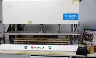
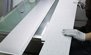
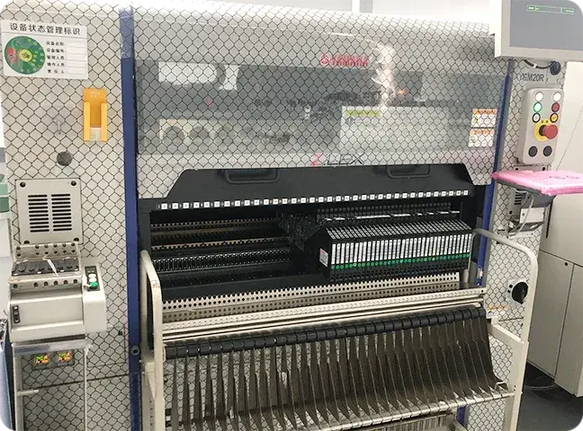
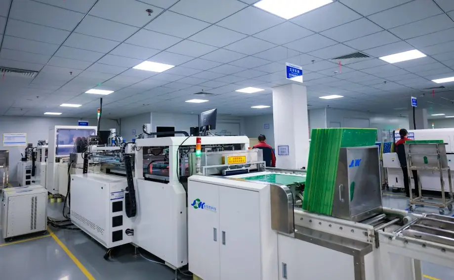
Our production lines cover the full PCB manufacturing process—from inner-layer imaging and lamination to drilling, plating, surface finish, and final inspection. These facilities support the technical requirements behind mSAP PCB manufacturing, including seed-layer formation, selective copper plating, and fine-line patterning.

PCB manufacturing facility 1
PCB manufacturing facility 2
PCB manufacturing facility 3
PCB manufacturing facility 4
PCB manufacturing facility 5
PCB manufacturing facility 6
PCB manufacturing facility 7
PCB manufacturing facility 8

Product Introduction

What Is mSAP PCB? A Manufacturing Approach for Fine-Line Circuits

mSAP (Modified Semi-Additive Process) PCB is a circuit board manufactured using a modified semi-additive process to create fine copper traces and support high-density interconnections. Unlike conventional subtractive etching, which forms circuits by removing unwanted copper from a thicker copper layer, mSAP builds copper selectively over a thin conductive seed layer. This approach helps control conductor geometry and enables finer circuit patterns for compact electronic designs.

The process typically involves substrate preparation, seed-layer formation, photoresist imaging, selective copper plating, resist stripping, seed-layer etching, and final inspection. Each stage requires careful control to maintain trace width, spacing, and dimensional consistency. Although mSAP and SAP share the semi-additive principle, their process implementations and manufacturing capabilities may differ. The appropriate method depends on the required circuit geometry, substrate, copper thickness, and production conditions.

For your mSAP PCB project, PCBMASTER can evaluate Gerber files, stack-up specifications, and critical dimensional requirements to assess manufacturing feasibility. Material selection and stack-up planning help align the design with electrical, thermal, and mechanical demands. Where applicable, prototype builds and dimensional measurements can support process validation before production planning. Relevant inspection records and quality documentation can also be provided according to the agreed project specifications.

Key Features

Key Features of mSAP PCB Technology

mSAP PCB technology combines selective copper plating and seed-layer removal to produce fine circuit patterns. These characteristics help you optimize routing density, accommodate compact component layouts, and meet demanding interconnection requirements.

Product Feature Description
Fine-Line Circuit Patterns Accommodate more routing paths within limited board space for compact electronic designs.
Thin Conductive Seed Layer Enables fine circuit formation with less unwanted base copper to remove.
Selective Copper Plating Builds copper on defined circuit areas to achieve the required conductor thickness.
Semi-Additive Circuit Formation Supports finer circuit geometries than conventional subtractive processing under suitable manufacturing conditions.
Controlled Trace Geometry Helps maintain specified trace widths and spacing for reliable circuit layout implementation.
Fine-Pitch Circuit Capability Facilitates routing between closely spaced component pads in high-density electronic designs.

Product Categories

Explore mSAP PCB Solutions for Different Design Requirements

PCBMASTER provides mSAP PCB solutions for fine-line circuits, high-density interconnections, multilayer designs, and fine-pitch components. Each solution is tailored to specific design requirements and manufacturing constraints.

Product Description
Fine-Line mSAP PCB Solutions Fit more circuit connections into limited substrate space with fine-line routing. Ideal for designs that require narrow traces and tight spacing to meet demanding layout and miniaturization requirements.
High-Density Interconnection mSAP PCB Solutions Accommodate more interconnections within a compact footprint. This solution helps you address limited routing space and complex connection requirements while evaluating the appropriate layer structure and circuit layout.
Multilayer mSAP PCB Solutions Manage complex routing across multiple layers to support more demanding interconnection designs. Stack-up planning helps you organize signal paths and power distribution while balancing board thickness, electrical requirements, and manufacturing feasibility.
Fine-Pitch Component mSAP PCB Solutions Route connections between closely spaced component pads, including those used in suitable BGA packages. Fine-line circuit formation helps you address tight package escape-routing requirements and make more effective use of available substrate space.

Build Smaller, Route Smarter with mSAP PCB Solutions.

PCBMASTER supports your fine-line PCB projects with engineering review, manufacturing process evaluation, and quality verification tailored to your design requirements.

Applications

mSAP PCB Applications Across Advanced Electronics

mSAP PCB technology enables fine-line circuits and dense interconnections, helping electronic designers connect more components within limited substrate space.

Application How mSAP PCB Is Used
Smartphones Enables fine-pitch connections between application processors, memory, and wireless components while reducing routing space in compact device assemblies.
Wearable Devices Integrates sensor, processor, and wireless circuitry into compact substrates, helping reduce circuit footprint in smartwatches and fitness trackers.
Communication Equipment Supports dense interconnections among RF, signal-processing, and control circuits in compact wireless communication modules.
Tablets and Computing Accommodates high-density connections between processors, memory, and supporting components in compact computing platforms.
Medical Electronics Enables fine-line routing for compact diagnostic, patient-monitoring, and portable medical devices where space is limited and reliability requirements must be met.
Imaging Equipment Connects image sensors, signal-processing circuits, and control components within compact camera and imaging modules.
Automotive Electronics Supports dense circuit routing in selected camera, radar, sensing, and control modules where compact layouts are required.
IoT Devices Integrates sensing, processing, and wireless communication connections within small devices with limited PCB or substrate area.
Advanced Packaging Forms fine-line interconnections between semiconductor dies, package terminals, and external circuitry in compatible IC package substrates, supporting high I/O density and compact package layouts.

Case Studies

mSAP PCB Engineering Solutions for Complex Designs

PCBMASTER serves customers across a wide range of industries, delivering mSAP PCB solutions that support fine-line circuitry, high-density interconnections, and compact electronic designs tailored to diverse application requirements.

01

Smartphone PCB Miniaturization

0.4 mm-Pitch BGASmartphoneMiniaturization

A smartphone manufacturer needed to integrate a high-performance processor and memory into a thinner device. The 0.4 mm-pitch BGA packages created dense escape-routing requirements, leaving insufficient routing space around component pads.

PCBMASTER optimized the BGA fan-out layout, redistributed signal connections across available layers, and used mSAP fine-line patterning in congested routing areas. The team also adjusted via placement and routing paths to reduce local congestion without unnecessarily increasing the substrate area.

These changes enabled more signal connections to fit within the available routing space. The resulting mSAP PCB served as the high-density interconnection platform for the processor, memory, and supporting components, supporting the smartphone's compact internal layout.

02

Wearable Device Circuit Integration

WearableSensor/Processor/WirelessCompact Substrate

A wearable device manufacturer needed to integrate sensor interfaces, processing circuits, power management, and wireless connectivity into a compact substrate. The restricted footprint made it difficult to route sensor signals and control connections while retaining sufficient space for power delivery.

PCBMASTER reorganized component placement and signal-routing paths, applied mSAP fine-line patterning to densely routed signal areas, and retained wider traces where power-current requirements demanded them. The team also optimized layer allocation to reduce routing conflicts between functional circuits.

This approach made better use of the available substrate area while accommodating the different routing requirements of signal and power circuits. The mSAP PCB connected the wearable's sensing, processing, power-management, and wireless functions within the compact device.

03

High-Density Communication Module

Communication ModuleRF + Signal Processing50 Ω Impedance

A communications equipment manufacturer needed a compact module combining RF, signal-processing, and control circuits. Dense routing competed with the need to maintain 50 Ω controlled impedance and appropriate signal-return paths.

PCBMASTER adjusted the signal-layer arrangement and reference-plane configuration, then coordinated trace geometry with the substrate's dielectric properties and copper thickness. Fine-line mSAP routing was applied where additional routing density was required, while critical RF traces were dimensioned to meet the specified impedance target rather than simply minimized.

The revised routing arrangement accommodated dense signal connections while preserving the design requirements for controlled impedance. The mSAP PCB provided the interconnection structure for the module's RF and processing circuits within the required footprint.

04

Compact Medical Electronics

Portable DiagnosticFine-PitchCompact Medical

A medical electronics manufacturer needed to fit sensing, data-processing, and communication circuits into a portable diagnostic device. Limited board space created routing bottlenecks around fine-pitch components, while the design also had to satisfy dimensional and assembly requirements.

PCBMASTER rearranged congested routing paths, applied mSAP fine-line patterning where narrow trace geometry was necessary, and adjusted the layer configuration to accommodate connections within the available area. The team also aligned substrate thickness, component clearances, and dimensional tolerances with the device's mechanical and assembly requirements.

These design changes helped accommodate the required circuit connections within the compact substrate while maintaining compatibility with the intended assembly process. The mSAP PCB served as the interconnection platform linking the device's sensing, processing, and communication functions.

Customer Reviews

What Customers Value in PCB Manufacturing Partnerships

With proven mSAP PCB manufacturing expertise, advanced fine-line capabilities, and reliable quality control, PCBMASTER helps customers bring complex, high-density designs to production with confidence.

Engineering Support
We had very little routing space around the BGA on our smartphone board. With this mSAP PCB project, getting the fine-line routing right was critical. I appreciated that PCBMASTER discussed fan-out routing, via placement, and layer allocation with our actual layout in mind, rather than simply focusing on minimum line width. That made the engineering discussions much more useful for our design decisions.
Michael Weber · Hardware Engineering Manager · Consumer Electronics · Germany Michael Weber · Hardware Engineering Manager · Consumer Electronics · Germany
Fine-Line Manufacturing Capability
Fine lines look good on a capability sheet, but the real question is whether the geometry can be manufactured consistently. For our mSAP PCB evaluation, we paid close attention to line width and spacing, copper thickness, and registration accuracy. I wanted to understand the manufacturing controls behind the specifications, not just the headline numbers. Those details are what matter when assessing a supplier for fine-line applications.
Emily Chen · Senior Process Engineer · Semiconductor Packaging · United States Emily Chen · Senior Process Engineer · Semiconductor Packaging · United States
Project Coordination and Delivery
The difficult part of our mSAP PCB project was keeping design revisions and prototype preparation aligned. A layout change can affect more than the design file—it can also change fabrication requirements and the production schedule. We needed clear communication on what had changed and what needed to be confirmed before moving forward. That was the part of the PCBMASTER collaboration I valued most.
DF Daniel Fischer · NPI Project Manager · Telecommunications · Sweden
Quality Assurance
I don't approve an mSAP PCB supplier based on general quality claims. I need agreed acceptance criteria, inspection results that can be reviewed, and documentation that matches the requirements of the order. For compact diagnostic electronics, those details are essential to our supplier assessment. My priority is knowing exactly how the delivered boards will be evaluated—not simply being told that quality comes first.
Sophie Laurent · Quality Assurance Manager · Medical Electronics · France Sophie Laurent · Quality Assurance Manager · Medical Electronics · France
10 FAQ

More About mSAP PCB

Explore these frequently asked questions to better understand mSAP PCB technology, evaluate manufacturing options, and make informed decisions about design, materials, costs, and supplier selection.

FAQ · 01

What Is the Difference Between mSAP PCB and Conventional PCB Fabrication?

Conventional subtractive PCB fabrication forms circuit patterns by removing unwanted copper from a copper-clad substrate. mSAP , by contrast, uses a seed layer and patterned plating to build copper traces, followed by removal of the exposed seed layer. This approach enables finer circuit geometries for applications where conventional etching may struggle to meet routing-density requirements. The appropriate process depends on the required line width and spacing, copper thickness, substrate type, and manufacturing capability.

FAQ · 02

SAP vs. mSAP: Which Process Fits Your Design?

SAP (Semi-Additive Process) and mSAP (Modified Semi-Additive Process) both use selective copper deposition to form fine circuit patterns. However, their process implementations, starting copper structures, and achievable feature dimensions can differ by manufacturing platform.

Comparison factor SAP mSAP
Circuit formation Builds copper selectively over a seed layer, followed by seed-layer removal Uses a modified semi-additive flow to form fine copper traces over a seed layer
Starting copper structure Typically uses a very thin seed layer Commonly uses a thin seed layer, with process details varying by manufacturer
Fine-line capability Suitable for very fine circuit geometries on compatible manufacturing platforms Supports fine-line patterns for high-density circuit designs
Typical application focus Advanced packaging substrates and applications requiring very fine circuit features Fine-line substrates and high-density interconnection designs
FAQ · 03

When Should I Choose mSAP PCB Instead of HDI PCB?

mSAP and HDI describe different aspects of PCB technology: mSAP is a circuit-patterning process, while HDI refers to high-density interconnection design and construction. They are not mutually exclusive options. Consider mSAP when your design requires fine copper traces and tight spacing; consider HDI features such as microvias, sequential lamination, and dense layer-to-layer connections when interconnection density is the primary challenge. A design may use both mSAP patterning and HDI construction.

FAQ · 04

Is mSAP PCB Suitable for Prototypes and Small-Volume Production?

Yes, mSAP PCBs can be used for prototypes and small-volume production when the design requirements justify the process and a suitable manufacturing route is available. However, advanced substrate processing, specialized materials, and process setup may increase initial costs compared with conventional PCB fabrication. Before ordering prototypes, confirm engineering feasibility, minimum order quantities, tooling or setup charges, and whether the prototype process can support the requirements of subsequent production.

FAQ · 05

What Design Files Are Required for an mSAP PCB Manufacturing Quote?

Prepare the Gerber or ODB++ manufacturing data, drill files, stack-up drawing, fabrication specifications, and bill of materials if assembly is included. For fine-line designs, provide the intended minimum line width and spacing, copper thickness, substrate material, finished thickness, surface finish, and any controlled-impedance requirements. If the design includes specialized packaging or substrate features, include the relevant drawings and tolerances. Complete documentation helps the manufacturer evaluate feasibility and identify potential cost or yield risks before quotation.

FAQ · 06

How Does Copper Thickness Affect mSAP PCB Design?

Copper thickness affects current-carrying capacity, resistance, thermal behavior, and the achievable fine-line geometry. Thicker conductors may be necessary for higher-current paths, but they can make very narrow trace formation more challenging depending on the plating and patterning process. Therefore, line width, spacing, and copper thickness should be specified together rather than selected independently. The final combination should be confirmed with the manufacturer against the electrical requirements and available process window.

FAQ · 07

Which Substrate Materials Are Used for mSAP PCBs?

Material selection depends on the application, electrical performance, dimensional stability, thermal requirements, and packaging structure. BT resin is commonly used in IC package substrates, while ABF build-up materials are used in many advanced semiconductor packaging applications. Other materials may be appropriate for different substrate designs. When selecting a material, confirm its compatibility with the manufacturing process, dielectric properties, thermal expansion behavior, moisture resistance, and the assembly or reliability requirements of the finished product.

FAQ · 08

How Can I Reduce mSAP PCB Manufacturing Costs?

The most effective approach is to match the design complexity to the actual electrical and packaging requirements. Avoid specifying unnecessarily narrow traces, excessive layer counts, overly tight tolerances, or specialized finishes without a clear functional reason. Standardizing material choices and panel dimensions where possible may also improve manufacturing efficiency. Share the intended production volume and expected product lifecycle with your manufacturer, because the most economical design for a prototype may differ from the best option for volume production.

FAQ · 09

What Quality Checks Should I Request for an mSAP PCB?

Quality requirements should reflect the product’s critical features rather than relying on a single generic inspection. Depending on the design, specify checks for line width and spacing, copper thickness, registration, dimensional tolerances, surface finish, and electrical continuity or isolation. Advanced substrates may also require additional inspection of fine circuit features and interconnection structures. Before production, agree on the applicable acceptance criteria, inspection methods, test coverage, and documentation required for lot release.

FAQ · 10

What Should I Confirm Before Placing an mSAP PCB Order?

Before approving production, confirm the final manufacturing data, stack-up, material grade, minimum line width and spacing, copper thickness, finished dimensions, surface finish, and applicable inspection requirements. Also clarify prototype or production quantities, lead time, quotation scope, testing documentation, and change-control procedures. If the design is intended for a regulated or safety-critical application, identify the relevant qualification requirements at the quotation stage. A documented engineering review and approved specification help prevent mismatches between design intent and the delivered substrate.


Related Products

Related PCB Products

Explore more PCB solutions to find the right fit for your design, performance, and manufacturing requirements.

Ready to Evaluate Your mSAP PCB Design?

Share your PCB design and manufacturing requirements with PCBMASTER. Our team can review the project scope, assess relevant process capabilities, and help you identify the next steps toward prototype validation or production.

Home Quote Order
Get Coupon