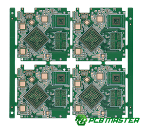
HDI PCB
Highly integrated, Ultra-thin, High-performance
High-Density Interconnect (HDI) PCBs deliver compact, thin and high-performance solutions for modern electronics, enabling smaller, faster and more powerful devices.

1000+ Global Clients Order Our HDI PCBs / Month
+%E6%8B%B7%E8%B4%9D.webp)
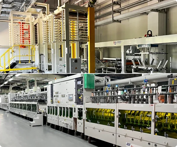
HDI Process Capability
4-64 layers PCB manufacturing
HDI Any-Level
Register now
Enjoy special - price orders for HDI PCB prototypes
Core Advantages of Our HDI PCB
We focus on balancing performance, cost and delivery to solve your project challenges.
Cost-Effective Pricing
Competitive prices with reliable quality as the premise — cost control, no performance loss, for R&D prototyping, small-batch & mass production.
-
4-layer(1-level) Blind via PCB: As low as $180 PCB prototype
without Buried via, S<0.3㎡, qty<20pcs -
6-layer(1-level) Blind via PCB: As low as $250 PCB prototype
without Buried via, S<0.3㎡, qty<20pcs
Fast Delivery
Accelerate your product launch with our efficient production capabilities.
- HDI PCBs delivered in as fast as 7 days
- Supports expedited service for urgent projects
- Consistent turnaround for all HDI types
Whether it is 4-layer 1level-HDI PCBs or Any Level HDI PCBs with more than 10 layers, the same fast delivery efficiency as ordinary quick-turn PCBs can be achieved, helping customers accelerate product R&D and market launch.
Strong Process Capability
Stable mass production to cover high-layer and multi-level needs.
- Layer range: 4-layer 1-level to 64-layer Any-level HDI PCBs
- Proficient in core processes
- Mature experience in Any-Layer HDI
Proficient in core processes such as fine circuits, microvias, stacked/staggered vias and Via-in-Pad; with mature experience in Any Level HDI production, meeting the needs of high-density and complex circuit designs.
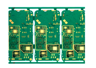
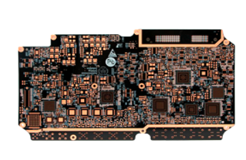
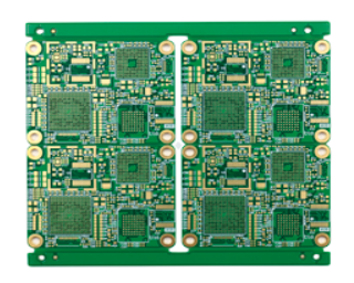
Our HDI PCB Products
Smaller Denser Thinner
Harness these three advantages in our HDI PCBs to create more compact, high-performance products that give you a competitive edge.
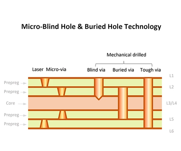
Core Technologies of HDI PCB
High-density interconnection in HDI PCBs relies on Laser drilling, Plated Through Hole, Lamination and fine circuit processes.
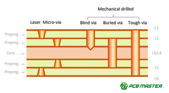
Micro-Blind Hole & Buried Hole Technology
Our advanced drilling technologies create precise connections between layers without sacrificing valuable board space.
- Blind Vias
- Buried Vias
-
The main methods for manufacturing blind vias and buried vias are:
Laser Drilling & Mechanical Drilling
Lamination Technology
Build-up is a core process for constructing micro-blind/buried-blind vias and improving HDI PCB density, with common methods including:
- Build-Up Method
- Sequential Lamination Method
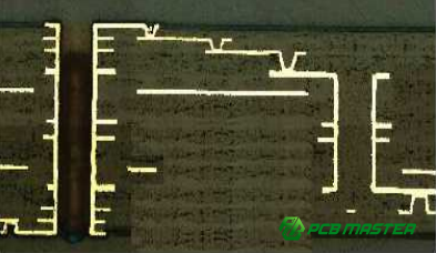
Fine Circuit Manufacturing
Micrometer-level precision with 1.5mil/1.5mil IC substrates for miniaturized electronics.
-
Micrometer-Level Control for HDI PCB Line Width & Spacing
-
Min track/spacing 1.5/1.5mil IC Substrates: Boost Integration, Fit Miniaturized Electronics
Electroplating & Hole-Filling
After the formation of micro-blind vias and circuits, professional electroplating processes are required to ensure electrical conductivity:
- Electroplating Treatment
- Electroplating Hole-Filling
- Quality Assurance
Typical HDI PCB Structures
HDI PCB structures are classified by microvia and lamination levels to match your design requirements.
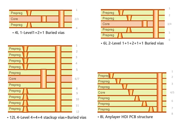
| Structure Level | Key Features |
|---|---|
| 1-Level HDI | Contains one layer of microvias (usually blind vias) |
| 2-Level HDI | Contains two layers of microvias, which can be stacked or staggered |
| 3-level/High-level HDI | Contains three or more layers of microvias, with a more complex structure |
| Any-Level HDI | Direct interconnection between any two layers can be achieved through laser microvias, making it the highest-density structure |
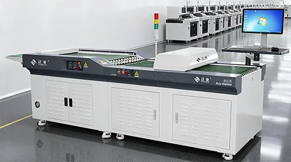
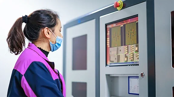
Quality Inspection Full-Process Control
We implement rigorous testing to guarantee HDI PCB quality, fully compliant with IPC Class 2 and Class 3 standards.
AOI aperture detection
-
Automatically inspects the tool diameter of drilling machines to prevent hole diameter deviation caused by tool wear;
-
AOI equipment scans the substrate after drilling to check for defects such as deviated drilling, missing holes and rough hole walls, preventing drilling issues from entering the next process.
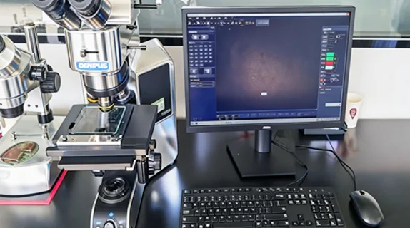
Metallographic Microscope, Plating Thickness Gauge
-
Metallographic Microscope
Analyzes the cross-sectional structure of hole copper and surface copper, verifying plating thickness (ensuring > 20μm) and uniformity.
-
Plating Thickness Gauge
Monitors the electroplating process in real time to prevent excessively thin/thick plating from affecting electrical performance.
AOI Line&Appearance Inspection
-
AOI After LDI Exposure
Checks for issues such as circuit short circuits, open circuits and line width deviation, ensuring circuit precision.
-
AOI for Finished Product Appearance
Fully scans the substrate surface to detect scratches, stains and component pad defects, ensuring appearance and circuit quality meet delivery standards.
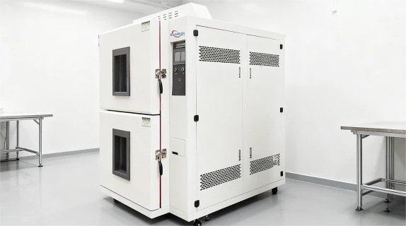
Reliability Testing
-
Key Test Items
Thermal Shock Test (-40℃ ~ 125℃, 1000 cycles), High-Temperature High-Humidity Aging Test;
-
Test Objective & Effect
Simulates harsh operating environments such as automotive electronics and medical equipment, testing the temperature resistance, humidity resistance and vibration resistance of HDI PCBs, verifying the stability of hole wall connections to ensure long-term reliable operation.
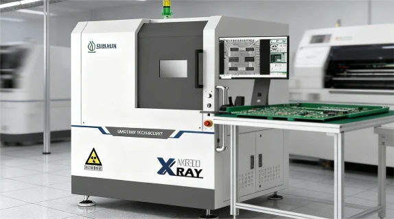
X-Ray Inspection
-
Core Function
Penetrates the substrate to inspect the internal connections of buried vias, checking for invisible defects such as voids and cold solder joints; simultaneously inspects the blind via filling rate (requiring ≥95%) to ensure the conductivity and stability of inner-layer interconnections.
Four-Wire Low-Resistance Test (Kelvin Test)
-
Position in Testing Process
A key link in PCB electrical performance testing
-
Testing Principle & Advantage
Through the separated design of "current lines + voltage lines", it eliminates interference from contact resistance/wire resistance, accurately measures low resistance ≤1Ω (e.g., copper foil circuits, blind/buried via conduction paths) and checks for hidden defects such as cold solder joints and thin hole copper, ensuring current transmission reliability.
.webp)
FAQs About HDI PCB
Have more questions? Our technical team is ready to help.
Contact Technical SupportWhy choose PCBMASTER for your blind/buried via PCB project?
PCBMASTER has decades of HDI manufacturing expertise, with advanced precision laser drilling and fully automated testing. Our engineers specialize in blind/buried via technologies, supporting early design phases for seamless concept-to-production transition—delivering high-performance, high-reliability PCBs.
PCBMASTER Blog & NEWS
We offer an all - inclusive experience. Let us take you on a journey to explore the world of wiring and get you familiar with us.
-
 MoreWhat Is HDI PCB? A Complete Guide to High-Density Interconnect Printed Circuit BoardsHDI PCB (High-Density Interconnect Printed Circuit Board) is an advanced PCB technology designed to accommodate more circuitry in a smaller space through the use of microvias, blind vias, buried vias, and fine-line routing. Compared with co...Jun 18, 2026
 -
MoreWhat Are the Different HDI PCB Levels? 1-Level vs. 2-Level vs. 3-Level vs. Any-Layer HDI Explainedlet dom = document.querySelector('.bg-white-light>.w-full.overflow-x-auto') dom.innerHTML = ` As electronic devices continue to become thinner, faster, and more compact, HDI (High Density Interconnect) technology has evolved from simple mic...Jun 15, 2026
-
MoreThrough-Hole PCB vs. HDI PCB: Is the Stack-Up Design Logic Fundamentally Different?While both through-hole PCBs and HDI (High-Density Interconnect) PCBs aim to achieve signal integrity, power integrity, manufacturability, and mechanical reliability, their stack-up design logic differs significantly due to the type of vias...Jun 9, 2026
-
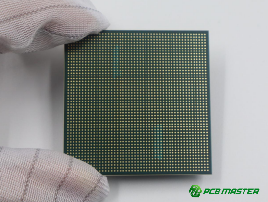
MoreBGA Routing and Via Design Rules: Best Practices for High-Density PCB LayoutsAs electronic products continue to integrate more functions into smaller form factors, BGA (Ball Grid Array) packages have become the preferred solution for high-pin-count devices. However, successful BGA implementation depends heavily on r...Jun 1, 2026