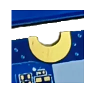
✓Uniform Nickel-Gold Surface for Fine-Pitch Components
✓Controlled ENIG Thickness and Surface Quality
✓Custom PCB Fabrication from Prototype to Production
✓Full Inspection and Engineering Support from PCBMASTER
Why PCBMASTER
Why Choose PCBMASTER for ENIG PCB?
PCBMASTER provides ENIG PCB manufacturing with a focus on surface finish consistency, coating quality, and solderability. By controlling the electroless nickel and immersion gold processes according to project specifications, we help you reduce surface-related assembly risks and achieve consistent results across production batches.
For fine-pitch components such as BGA and QFN, PCBMASTER supports ENIG PCB fabrication designed to meet demanding pad flatness and assembly requirements. Whether you need single-sided, double-sided, or multilayer ENIG PCBs, we customize board thickness, copper weight, stack-up, and other specifications to match your design and application.
PCBMASTER combines ENIG PCB fabrication with SMT assembly, PCBA services, and bare PCB fabrication to finished circuit board assemblies. Our quality management systems comply with ISO 9001 and IATF 16949 requirements, supporting consistent manufacturing processes and quality control.
Electrical testing and visual inspections are performed according to applicable product specifications. Relevant UL certification documentation and RoHS compliance information can be provided where applicable to your product and project requirements.
With stable material sourcing, PCBMASTER helps you maintain material consistency and reduce supply-related production risks. Our engineering team provides one-on-one support from design review and DFM evaluation to manufacturing and delivery, helping you move your ENIG PCB project from prototype to production with greater confidence.
Product Introduction
What Is an ENIG PCB?
An ENIG PCB (Electroless Nickel Immersion Gold Printed Circuit Board) uses a chemical nickel layer and a thin immersion gold layer to protect exposed copper pads and provide a solderable surface. This finish offers a flat surface suitable for fine-pitch components, including BGA and QFN packages, and helps protect pads against oxidation during appropriate storage conditions.
The ENIG process typically involves surface cleaning, micro-etching, activation, electroless nickel deposition, immersion gold deposition, rinsing, drying, and final inspection. The nickel layer acts as a barrier between the copper and gold, while the gold layer protects the nickel surface. However, ENIG performance depends on coating thickness, bath chemistry, process control, and nickel-gold interface quality. Poor process control can lead to defects such as black pad, potentially affecting solder joint reliability.
PCBMASTER supports your ENIG PCB project from initial requirement review and DFM assessment to material selection, stack-up planning, and manufacturing specification review. Our engineering team evaluates pad geometry, solder mask design, board structure, and surface finish requirements to help identify potential manufacturing issues before production. Inspection and testing are conducted according to applicable specifications, with PCB assembly support available to help you move from bare boards to finished PCBAs.
ENIG PCB combines a flat surface finish with a protective nickel-gold coating to meet demanding PCB assembly requirements. Its surface characteristics help you accommodate fine-pitch components, protect exposed pads during storage, and achieve consistent assembly results across a wide range of electronic applications.
Feature
Description
Flat Surface Finish
A relatively flat ENIG surface helps you achieve more uniform solder paste deposition and component placement, particularly for fine-pitch packages such as BGA and QFN.
Nickel-Gold Layer Structure
Combining a nickel barrier with a thin gold coating provides complementary protective functions, helping preserve exposed pad surfaces during storage and before assembly.
Oxidation Protection
The immersion gold layer protects the underlying nickel surface under appropriate storage conditions, helping maintain pad surface quality before soldering.
Solderable Surface
ENIG provides a solderable surface for compatible assembly processes, supporting solder joint formation when coating quality, solder paste, and reflow parameters are properly controlled.
Copper Diffusion Barrier
By separating the copper substrate from the gold coating, the electroless nickel layer limits copper diffusion and helps maintain surface finish integrity.
Consistent Surface Finish
Properly controlled ENIG processing helps achieve uniform coating coverage across exposed pads, providing consistent surface conditions for component assembly and production quality control.
Product Categories
ENIG PCB Types
PCBMASTER offers a wide range of ENIG PCB options to match your board structure, component layout, electrical performance, and application requirements, helping you find the right solution for your project.
Product
Description
Fine-Pitch ENIG PCB
Achieve reliable soldering for BGA, QFN, and other fine-pitch components with a flat surface finish that supports precise placement and consistent solder paste deposition.
Multilayer ENIG PCB
Integrate complex circuits into a compact board with multiple signal, power, and ground layers, giving you greater routing flexibility and design freedom.
HDI ENIG PCB
Fit more functionality into limited space with microvias and fine routing, making it suitable for compact electronics with high component density.
Rigid-Flex ENIG PCB
Combine rigid and flexible circuit sections to reduce connector requirements, save assembly space, and simplify interconnections in compact electronic products.
Heavy Copper ENIG PCB
Support high-current circuit designs with increased copper thickness, helping you meet power distribution and current-carrying requirements while maintaining a solderable surface for assembly.
High-Frequency ENIG PCB
Develop RF and wireless circuits with suitable high-frequency materials and controlled-impedance design, helping you meet demanding signal transmission requirements.
PCBMASTER offers customizable ENIG PCB specifications to match your circuit design, component layout, assembly process, and application requirements. The following parameters help you define the right board configuration for your project. Final capabilities depend on board structure, copper thickness, manufacturing process, and order requirements.
Parameter
What You Can Specify
PCBMASTER Options
Layer Count
Number of layers based on routing density and circuit complexity
Up to 64 layers for rigid PCBs, depending on design and process
Board Thickness
Finished thickness and tolerance
0.5–6.0 mm for applicable PCB configurations.
Copper Weight
Inner and outer copper weight according to current and thermal requirements
Inner layers: 0.5–40 oz; outer layers: 1–10 oz for applicable configurations.
Minimum Trace Width and Spacing
Trace width and spacing based on routing density and copper thickness
3/3 mil to 1/1 mil, depending on PCB type and manufacturing process.
Minimum Drill Size
Mechanical drill diameter, laser-drilled microvia size, and via structure
0.05 mm for applicable PCB technologies; minimum sizes vary by drilling method and board structure.
ENIG Nickel Thickness
Nickel thickness according to the applicable surface-finish specification
Typically 3–6 μm.
ENIG Gold Thickness
Immersion gold thickness according to solderability and finish requirements
Board length, width, outline, and dimensional tolerance
Custom dimensions and tolerances depend on board type and manufacturing process.
Electrical Testing Requirements
Electrical continuity and isolation testing, acceptance criteria, and applicable quality class
Electrical continuity and isolation testing; IPC Class 2 or Class 3 acceptance requirements, as specified for the project.
Get the Right ENIG PCB for Your Project
Looking for ENIG PCBs with consistent surface quality and reliable manufacturability? Contact PCBMASTER to discuss your specifications, get expert engineering support, and receive a tailored quotation for your project.
ENIG PCBs support a wide range of electronic applications, offering a flat solderable surface, pad protection, and compatibility with fine-pitch SMT assembly to meet different product design requirements.
Industry
How ENIG PCB Is Used
Automotive Electronics
Supports fine-pitch ECUs, sensor modules, and vehicle control boards by providing a flat solderable surface for reliable component assembly.
Industrial Control
Protects exposed pads during storage and provides a solderable finish for PLCs, motor controllers, and industrial automation circuits.
Telecommunications
Supports fine-pitch components and dense multilayer layouts in communication equipment, helping accommodate compact designs and complex interconnections.
Medical Electronics
Provides a flat surface for assembling fine-pitch components in diagnostic devices, patient monitoring systems, and other precision medical electronics.
Consumer Electronics
Supports compact PCB layouts and fine-pitch SMT components in smartphones, wearables, and home electronics while helping maintain consistent solderable pad quality.
Computing and Servers
Facilitates BGA and other fine-pitch component assembly in servers, processors, and computing hardware through its relatively flat surface finish.
Power Electronics
Provides a solderable surface for power-control circuits, while copper thickness, board structure, and thermal design are tailored to current and heat dissipation requirements.
IoT and Sensors
Supports compact sensor and wireless modules by providing a flat surface for densely placed components and protecting exposed pads before assembly.
Aerospace Electronics
Provides a controlled surface finish for avionics and aerospace circuit boards, supporting solderability and pad protection when manufacturing, testing, and documentation meet project-specific requirements.
PCBMASTER has supported customers across a wide range of industries with ENIG PCB solutions tailored to their specific design requirements, manufacturing challenges, and application needs.
01
Automotive Control Module ENIG PCB
An automotive electronics customer needed an ENIG PCB for a control module featuring fine-pitch BGA components. The main challenges were maintaining pad consistency, achieving reliable soldering, and controlling batch-to-batch variation. The project used an illustrative 8-layer design with a 1.6 mm finished thickness and 1 oz outer-layer copper.
PCBMASTER reviewed the BGA footprints, solder mask openings, and stack-up during DFM assessment. Our engineers also defined the ENIG coating requirements, with a target nickel thickness of 3–6 μm and gold thickness of 0.05–0.10 μm. Manufacturing quality checks included surface inspection, dimensional verification, and electrical continuity and isolation testing.
The finished PCB provided stable electrical interconnections for the control module and a flat solderable surface for fine-pitch assembly. These manufacturing controls helped address board-level risks before the PCB entered the customer's assembly process.
02
Industrial Controller Multilayer ENIG PCB
An industrial automation customer required a multilayer ENIG PCB to integrate control logic, signal interfaces, and power distribution. The main challenges involved dense routing, layer registration, and consistent surface finish quality. The illustrative board configuration included 10 layers, a 2.0 mm finished thickness, 1 oz outer-layer copper, and 0.5 oz inner-layer copper.
PCBMASTER's engineers reviewed the stack-up, trace geometry, via locations, and drilling requirements before fabrication. The team checked whether the proposed 4/4 mil minimum trace width and spacing matched the selected construction and copper thickness. The manufacturing inspection plan covered layer registration, board dimensions, ENIG surface appearance, and electrical continuity and isolation.
These measures helped verify that the multilayer board met its defined fabrication requirements. The completed PCB served as the electrical platform connecting the controller's processing, communication, and power circuits within a single assembly.
03
Medical Instrumentation ENIG PCB
A medical instrumentation customer needed a compact ENIG PCB for a diagnostic or monitoring device using fine-pitch SMT components. The key challenges were maintaining pad quality in a dense layout and providing inspection records for quality traceability. The illustrative design used 6 layers, a 1.2 mm finished thickness, and 0.5 oz copper on the inner and outer layers.
PCBMASTER reviewed component footprints, solder mask openings, and board dimensions to identify potential fabrication and assembly issues. Our engineers specified the ENIG coating requirements and incorporated visual inspection, dimensional checks, and electrical continuity and isolation testing into the quality plan. Lot identification and inspection records were also aligned with the project's documentation requirements.
The finished PCB provided the interconnections for sensing, signal processing, and control circuits. Consistent pad conditions supported component assembly, while documented inspection results helped the customer manage incoming quality checks and manufacturing traceability.
04
Networking Equipment HDI ENIG PCB
A networking equipment customer required an HDI ENIG PCB for fine-pitch BGA components and dense interconnections within a limited board area. The main challenges were coordinating microvia structures, fine-line routing, and multilayer registration. The illustrative design featured 10 layers, a 1.0 mm finished thickness, 0.5 oz copper, 0.10 mm laser-drilled microvias, and 3/3 mil minimum trace width and spacing.
PCBMASTER reviewed the HDI stack-up, microvia placement, BGA pad geometry, and routing constraints during DFM assessment. Our engineers evaluated the microvia structure against the board construction and established inspection requirements for dimensional accuracy, ENIG surface quality, and electrical continuity and isolation. Microsection analysis was included where required to verify relevant plated interconnections.
The completed HDI PCB enabled dense connections between processors, memory, and communication components. Coordinating HDI fabrication and ENIG finish requirements helped prepare the board for fine-pitch assembly within the customer's space constraints.
Customer Reviews
ENIG PCB Customer Testimonials
PCBMASTER has supplied ENIG PCBs to customers across multiple industries, earning positive feedback for quality, engineering support, and reliable service.
Surface Finish Consistency
★★★★★
When I review an ENIG PCB, I pay close attention to pad condition and nickel-gold finish consistency. These details matter when we evaluate solderability and investigate assembly issues. PCBMASTER discussed the finish specifications and inspection criteria with us before production, which made it easier to align our quality requirements with the manufacturing process.
The main concern with our board was the fine-pitch BGA layout. There was little room for errors in pad geometry or solder mask openings, so I wanted the fabrication details checked before releasing the design. PCBMASTER reviewed these points with us, helping us address manufacturing considerations before the boards reached SMT assembly.
Daniel Brooks · Hardware Design Engineer · Telecommunications · United StatesDelivery and Communication
★★★★★
From a purchasing perspective, I need straightforward answers about specifications, lead times, and order status. I don't want to chase multiple people just to clarify a manufacturing detail. PCBMASTER's communication helped our purchasing and engineering teams coordinate the ENIG PCB order more efficiently.
Sophie Martin · Procurement Manager · Industrial Automation · FrancePrototype-to-Production Support
★★★★★
A prototype is only one milestone; the bigger question is whether the design can move smoothly toward production. I needed our ENIG PCB requirements reviewed early enough to avoid unnecessary changes later. PCBMASTER helped us work through the manufacturing details at the development stage, giving our team a clearer basis for planning the next phase.
Oliver Schmidt · Electronics Project Manager · Medical Electronics · Netherlands
Have questions about ENIG PCB selection, performance, or manufacturing? Find practical answers to help you make informed decisions for your project.
Knowledge · 01
Is ENIG PCB suitable for both prototype and mass production?
Yes. ENIG PCB is suitable for prototypes, pilot runs, and mass production when the design, surface-finish specifications, and manufacturing process are properly controlled. It is particularly useful when a project requires a flat solderable surface, fine-pitch components, or boards that may need to be stored before assembly.
Knowledge · 02
How do I know if ENIG is worth the additional cost?
ENIG is worth considering when component pitch, pad coplanarity, storage conditions, or assembly requirements justify its higher cost compared with simpler finishes such as HASL. For basic designs with larger-pitch components and tight budgets, HASL or another suitable finish may be sufficient. Evaluate the total manufacturing and assembly requirements rather than comparing surface-finish prices alone.
Knowledge · 03
Can ENIG PCBs be stored before soldering?
Yes, but storage conditions and packaging matter. Keep ENIG PCBs in their original protective packaging, in a clean, dry environment, and follow the supplier’s recommended storage period and handling instructions. Before assembly, inspect the boards for contamination, physical damage, or other signs of surface degradation. Do not assume that ENIG makes a PCB immune to improper storage.
Knowledge · 04
Does ENIG affect high-frequency signal performance?
ENIG can influence high-frequency conductor losses because the finish contains a nickel layer, which has different electrical properties from copper. The significance depends on frequency, trace geometry, surface-finish thickness, and signal-loss requirements. For demanding RF or high-speed designs, evaluate the complete stack-up and transmission-line structure with the PCB manufacturer rather than selecting ENIG based on flatness alone.
Knowledge · 05
Can ENIG be used with press-fit connectors or solderless contacts?
Not automatically. ENIG is primarily selected for solderable pads and component assembly. Press-fit contacts, edge connectors, and other repeated-contact interfaces may require finishes specifically suited to their mechanical wear, contact resistance, and mating-cycle requirements. Confirm the connector manufacturer’s finish recommendations before choosing ENIG for these areas.
Knowledge · 06
Is ENIG suitable for wire bonding?
Standard ENIG is not automatically suitable for every wire-bonding process. Wire bonding depends on the bonding method, wire material, bond-pad metallurgy, surface cleanliness, and process parameters. If your design requires gold or aluminum wire bonding, specify the bonding process and pad requirements before fabrication so the appropriate surface finish can be evaluated.
Knowledge · 07
What causes black pad in ENIG PCBs?
Black pad is a surface-finish defect associated with excessive or abnormal nickel corrosion during the immersion-gold process. It can weaken the nickel-gold interface and contribute to solder-joint reliability problems. Prevention depends on controlling nickel deposition, gold immersion chemistry, bath condition, and process parameters. If the application has stringent reliability requirements, discuss the manufacturer’s process controls and relevant inspection methods.
Knowledge · 08
Can ENIG PCBs be reworked or repaired?
Yes, in many cases, but rework must be controlled. Removing and replacing components can damage pads or alter the local surface condition if excessive heat or mechanical force is applied. The appropriate method depends on the component package, board construction, pad geometry, and rework temperature profile. For fine-pitch BGA or high-value assemblies, use a qualified rework process and inspect the repaired joints.
Knowledge · 09
Does ENIG eliminate the need for solderability testing?
No. ENIG provides a solderable surface, but it does not guarantee acceptable solder joints under every condition. Solderability can be affected by surface contamination, finish quality, storage history, solder paste, and the reflow profile. For critical applications or long-stored boards, define suitable solderability verification and assembly acceptance criteria based on the applicable product requirements.
Knowledge · 10
What information should I provide when requesting an ENIG PCB quotation?
Provide the Gerber or other accepted fabrication files, drill data, board dimensions, layer count, stack-up, copper weights, material requirements, quantity, and required delivery date. Also specify ENIG thickness requirements if defined, impedance targets, IPC class, testing requirements, and any special component or assembly constraints. Complete information helps the manufacturer assess manufacturability, identify technical risks, and prepare a more accurate quotation.
Get a Custom ENIG PCB Quote for Your Project
Share your PCB design files, surface finish requirements, and production targets with PCBMASTER to receive engineering feedback and a manufacturing quotation.
We use necessary cookies to ensure basic site functionality (browsing, quotation, login) and optional analytics cookies to optimize our service.
Your data is strictly confidential and will never be sold or shared with any third party.
Your consent is voluntary and revocable.
We use necessary cookies to ensure basic site func...