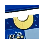
✓Excellent Solderability for Fine-Pitch Components and BGA Packages
✓Flat, Uniform Surface for Advanced SMT Assembly
✓Reliable Nickel-Palladium-Gold Layer Structure
✓Custom ENEPIG PCB Fabrication with Engineering Support
Why PCBMASTER
Why Choose PCBMASTER as Your ENEPIG PCB Manufacturer?
When you choose PCBMASTER for ENEPIG PCB manufacturing, you benefit from carefully controlled surface finishing processes involving electroless nickel, electroless palladium, and immersion gold deposition. We focus on process control to achieve consistent plating thickness, surface uniformity, and finish quality according to your project specifications.
Our stable material supply chain and standardized production procedures support reliable PCB manufacturing across different production batches. With advanced fabrication capabilities, we manufacture diverse board structures, including HDI, multilayer, and rigid-flex PCBs, to accommodate complex designs and demanding electronic applications.
Quality is integrated throughout our manufacturing process. From electrical testing and visual inspection to final quality verification, we implement systematic controls to ensure product quality. Our ISO 9001 and IATF 16949 quality management system certifications, UL certification, and RoHS compliance demonstrate our commitment to manufacturing quality, product safety, and environmental responsibility.
You also receive dedicated engineering and DFM support. Our engineers review your PCB designs, assess manufacturing feasibility, identify potential production risks, and provide technical recommendations to help optimize manufacturability, quality, and production efficiency.
Product Introduction
What Is ENEPIG PCB Surface Finish?
ENEPIG (Electroless Nickel Electroless Palladium Immersion Gold) is a chemical surface finish used in PCB manufacturing. It deposits three metallic layers—nickel, palladium, and gold—onto exposed copper pads. This layered structure protects the copper surface while providing a flat, solderable finish for advanced electronic assembly applications.
Each layer serves a specific purpose. The electroless nickel layer acts as a diffusion barrier between copper and the outer metallic layers. The electroless palladium layer provides an additional barrier between nickel and gold, helping reduce nickel corrosion-related defects. The immersion gold layer protects the underlying palladium from oxidation and maintains surface integrity.
The ENEPIG manufacturing process typically involves copper surface preparation, micro-etching, cleaning, electroless nickel plating, electroless palladium plating, immersion gold deposition, rinsing, drying, and final inspection. Proper control of bath chemistry, deposition time, and individual layer thickness is essential to achieving consistent results.
For your PCB assembly projects, ENEPIG offers a flat surface suitable for fine-pitch components, BGA, and CSP packages. It also supports selected gold wire bonding applications and helps reduce the risk of black pad defects associated with excessive nickel corrosion.
If your design requires reliable solderability, fine-pitch compatibility, and potential wire bonding capability, ENEPIG is a surface finish worth considering.
ENEPIG PCB combines electroless nickel, electroless palladium, and immersion gold to create a uniform metallic finish with distinct functional layers. Its surface characteristics and protective properties help you meet demanding PCB fabrication and assembly requirements.
Feature
Description
Flat and Uniform Surface
A smooth, level finish across exposed copper pads supports precise solder paste printing and fine-pitch component placement in your PCB assembly projects.
Three-Layer Metallic Structure
The nickel, palladium, and gold layers perform distinct functions, providing your PCB pads with multiple levels of protection and a functional metallic surface.
Distinct Metallic Layer Composition
Each metallic layer contributes different material properties, giving you a surface finish that combines nickel’s barrier function, palladium’s intermediate protection, and gold’s surface protection.
Excellent Corrosion Resistance
The multilayer metallic structure helps reduce corrosion-related risks, keeping your PCB pads in better condition throughout manufacturing, storage, and assembly.
Oxidation Protection
The immersion gold layer protects the underlying palladium surface from oxidation, helping preserve surface integrity and solderability under appropriate storage conditions.
Solderable Metallic Surface
The metallic finish provides a suitable surface for solder joint formation, supporting your SMT assembly requirements when compatible solder alloys and process parameters are used.
Product Categories
Explore Our ENEPIG PCB Types
Explore our ENEPIG PCB types based on board structure and assembly requirements. From multilayer and high-density designs to specialized component packaging and fine-pitch assembly, our ENEPIG PCB solutions support a wide range of electronic manufacturing needs.
ENEPIG PCB by Board Structure
Choose an ENEPIG PCB based on your board architecture, interconnection density, and mechanical requirements.
Product
Description
ENEPIG Multilayer PCB
Designed for complex circuits requiring multiple conductive layers, reliable interconnections, and a flat ENEPIG surface finish for component assembly.
ENEPIG HDI PCB
Combines high-density interconnection technology with ENEPIG surface finishing to support compact layouts, fine-pitch components, and advanced electronic designs.
ENEPIG Rigid-Flex PCB
Integrates rigid and flexible circuit sections into one board structure, providing design flexibility for electronic assemblies with limited installation space.
ENEPIG Flexible PCB
Combines a flexible circuit structure with an ENEPIG surface finish for compact electronic designs that require bending capability and reliable pad protection.
ENEPIG PCB by Assembly Requirements
Select an ENEPIG PCB according to your component packaging, pad layout, and assembly process requirements.
Product
Description
ENEPIG BGA PCB
Suitable for PCB designs using ball grid array components, where consistent pad surfaces and reliable solder joint formation are important for assembly quality.
ENEPIG CSP PCB
Designed for compact assemblies using chip-scale packages, supporting space-efficient layouts and the surface requirements of miniature electronic components.
ENEPIG Wire Bonding PCB
Uses a nickel-palladium-gold surface structure that can support compatible gold wire bonding processes, subject to bonding parameters and pad design requirements.
ENEPIG Fine-Pitch PCB
Features a flat surface finish that supports fine-pitch component placement and solder paste printing in high-density electronic assemblies.
ENEPIG PCB surface finish supports a range of electronic applications that require reliable soldering, fine-pitch assembly, corrosion protection, or wire bonding. Its nickel-palladium-gold layer structure makes it suitable for selected high-density and advanced electronic manufacturing requirements.
Industry
How ENEPIG PCB Is Used
Telecommunications
High-density communication equipment often incorporates fine-pitch processors, RF modules, and signal-processing components. ENEPIG offers a flat, solderable pad surface that accommodates these assembly requirements while protecting exposed copper.
Automotive Electronics
Automotive control units, sensor modules, and power management systems rely on consistent PCB assembly quality. The nickel-palladium-gold structure protects exposed copper pads and helps maintain surface integrity during storage and assembly.
Medical Electronics
Diagnostic equipment, patient monitors, and medical imaging systems often require compact circuit layouts with densely populated components. ENEPIG’s flat surface finish facilitates fine-pitch component assembly and reliable solder joint formation.
Aerospace Electronics
Avionics, navigation systems, and aerospace communication equipment demand carefully controlled electronic manufacturing processes. ENEPIG offers a uniform metallic surface for precision soldering and selected wire bonding applications.
Semiconductor Packaging
Advanced semiconductor packages require precise interconnections between dies, substrates, and external circuits. ENEPIG accommodates selected fine-pitch soldering and gold wire bonding processes through its nickel-palladium-gold layer structure.
Industrial Automation
PLCs, motor controllers, industrial sensors, and monitoring systems operate in demanding manufacturing environments. ENEPIG’s multilayer metallic finish helps protect PCB pads against corrosion and preserves solderability under appropriate storage and handling conditions.
Consumer Electronics
Smartphones, wearable devices, digital cameras, and other compact products require space-efficient PCB layouts. The flat ENEPIG finish accommodates fine-pitch components and densely populated assembly designs.
Networking Equipment
Routers, switches, server network cards, and data communication modules contain complex circuits with high component density. ENEPIG provides a uniform pad surface for assembling fine-pitch processors, memory devices, and other advanced components.
Test and Measurement
Oscilloscopes, spectrum analyzers, signal generators, and precision instruments rely on accurately assembled electronic circuits. ENEPIG helps maintain clean, solderable pad surfaces for densely populated boards and precision electronic assemblies.
ENEPIG for Gold Wire Bonding Applications
Wire bonding deserves particular attention because it is one of the important application advantages of ENEPIG compared with conventional ENIG.
The nickel-palladium-gold structure makes ENEPIG suitable for selected gold wire bonding applications. The electroless palladium layer acts as a barrier between nickel and gold, helping reduce nickel corrosion-related defects while providing a metallic surface for compatible bonding processes.
This makes ENEPIG a potential choice for semiconductor packaging, aerospace electronics, medical devices, and specialized electronic modules that require both soldering and wire bonding.
Actual bonding performance depends on the gold layer properties, pad cleanliness, wire material, bonding force, temperature, and ultrasonic energy. These parameters should be evaluated against your specific wire bonding process before production.
Every Layer Matters. Every Process Counts.
From PCB fabrication to final inspection, PCBMASTER focuses on process consistency, engineering precision, and dependable quality to support your ENEPIG PCB projects from prototype to production.
ENEPIG PCB Manufacturing Solutions for Real-World Applications
ENEPIG PCB is used in a wide range of electronic applications, from high-density communication equipment and automotive control systems to medical devices and semiconductor packaging. PCBMASTER works with customers across these industries to address their specific PCB design, surface finishing, and assembly requirements.
01
ENEPIG PCB for High-Density BGA Assembly
A customer developing a high-performance computing board needed a multilayer PCB with multiple fine-pitch BGA components. The closely spaced solder pads required a flat and uniform surface to support accurate solder paste printing and consistent component attachment.
The main challenge was maintaining consistent pad conditions across densely arranged BGA footprints while controlling the risk of nickel corrosion-related defects. Any irregularities in the surface finish could affect solder joint formation and assembly quality.
PCBMASTER's engineering team first reviewed the BGA pad layout, solder mask openings, copper pad dimensions, and surface finish requirements. During fabrication, the copper pads underwent surface cleaning and micro-etching before electroless nickel, electroless palladium, and immersion gold deposition. The plating process was monitored to maintain the specified layer characteristics. Finished boards were inspected for surface appearance, pad condition, and compliance with the agreed ENEPIG specifications.
This process provided the customer with a flat, solderable surface for fine-pitch BGA assembly, helping reduce surface-related manufacturing risks and improve assembly consistency.
02
ENEPIG PCB for Semiconductor Wire Bonding
A semiconductor module developer needed a PCB substrate with both conventional soldering pads and gold wire bonding areas. The surface finish had to provide suitable bonding characteristics while protecting exposed copper from oxidation and corrosion.
The challenge was ensuring that the ENEPIG layer structure was compatible with the customer's gold wire bonding process. Nickel and palladium deposition, gold layer characteristics, pad cleanliness, and bonding parameters all influenced the final bonding interface.
PCBMASTER's engineering team reviewed the bonding pad dimensions, pad spacing, copper exposure, and customer's wire bonding specifications before production. The copper surfaces were cleaned and micro-etched, followed by electroless nickel and palladium deposition and immersion gold finishing. The team also checked the finished pad surfaces and plating specifications. For process validation, sample boards should undergo bonding tests using the customer's actual gold wire, bonding force, temperature, and ultrasonic settings.
The ENEPIG finish offered a suitable metallic surface for compatible gold wire bonding while retaining solderable areas for other components, helping simplify the surface finish requirements of the electronic module.
03
ENEPIG HDI PCB for Compact Medical Electronics
A medical electronics developer needed a compact HDI PCB for a portable diagnostic device. The design incorporated multiple functional circuits, fine-pitch components, and microvia interconnections within a limited board footprint.
The main challenge was coordinating HDI fabrication with ENEPIG surface finishing. Microvia geometry, pad dimensions, copper surface condition, and plating compatibility all required attention to prevent manufacturing defects and preserve assembly quality.
PCBMASTER's engineering team reviewed the stack-up, microvia locations, via-in-pad structures, copper thickness, and component pad layout before fabrication. The HDI process included laser drilling, desmear, copper deposition, and sequential build-up operations according to the approved design. Before ENEPIG plating, exposed copper pads were cleaned and micro-etched to prepare the surface for uniform deposition. Electroless nickel, palladium, and immersion gold were then applied in sequence. Final inspections focused on microvia quality, pad condition, surface finish appearance, and compliance with the specified dimensions.
The resulting HDI structure allowed more interconnections within a smaller PCB footprint, while ENEPIG provided a flat, solderable surface for assembling miniature electronic components.
04
ENEPIG PCB for Automotive Electronic Control Systems
An automotive electronics developer required multilayer PCBs for an electronic control system integrating processing units, sensor interfaces, and power management circuits. The project required repeatable surface finish quality and consistent manufacturing results across production batches.
One major challenge was maintaining consistent ENEPIG deposition across multiple panels and production runs. Variations in copper preparation, plating bath chemistry, and deposition conditions could affect metallic layer characteristics and subsequent soldering performance.
PCBMASTER's engineering team reviewed the stack-up, material specifications, copper pad design, and ENEPIG thickness requirements before production. During manufacturing, copper surface preparation was controlled to remove contaminants and ensure suitable plating conditions. The electroless nickel and palladium baths were monitored for key process parameters, including chemical concentration, temperature, and operating conditions. Immersion gold deposition was then performed according to the specified process window. Finished boards underwent dimensional inspection, visual surface inspection, and verification of plating specifications. Production records were maintained to support batch traceability.
These manufacturing controls helped maintain consistent ENEPIG pad conditions across production lots, providing a stable solderable surface for automotive electronic control board assembly.
Customer Reviews
What Our Customers Say About PCBMASTER’s ENEPIG PCB
Customers across various industries value PCBMASTER’s ENEPIG PCB solutions for our engineering support, product quality, delivery performance, and responsive service.
Engineering Support
★★★★★
Honestly, the engineering feedback was one of the reasons we moved forward with PCBMASTER. Our ENEPIG PCB design had several details that needed a closer look before production. Their engineers reviewed the files carefully and gave us practical suggestions instead of generic comments. That kind of technical input saves time on our side.
Michael Turner | Hardware Engineering Manager | Telecommunications | United StatesProduct Quality
★★★★★
For us, surface finish quality is not just about appearance. It has to perform well during assembly. The ENEPIG PCB boards we evaluated from PCBMASTER showed a uniform finish, and the soldering performance met our project expectations. We pay close attention to consistency, so this was an important factor in our supplier evaluation.
Dr. Sophie Weber | Quality Assurance Engineer | Medical Electronics | GermanyDelivery Performance
★★★★★
Production schedules can change quickly in automotive electronics. What I appreciated was that PCBMASTER kept us updated on the ENEPIG PCB order without us having to ask repeatedly. The coordination was clear, and it helped our purchasing team manage the timeline with fewer surprises.
I prefer working with suppliers who are easy to reach and straightforward to deal with. Whenever we had questions about our ENEPIG PCB order, the PCBMASTER team responded promptly and followed up on the details. It made the project feel much easier to manage. Good service really does make a difference.
Marco Bianchi | Purchasing Director | Industrial Automation | Italy
Have more questions about ENEPIG PCB? Explore these frequently asked questions to better understand its manufacturing considerations, assembly compatibility, performance factors, and key points to consider when sourcing ENEPIG PCBs.
Knowledge · 01
What Is the Difference Between ENEPIG and ENIG PCB?
ENEPIG and ENIG both use electroless nickel and immersion gold, but ENEPIG adds an electroless palladium layer between nickel and gold. This additional layer acts as a barrier that helps reduce nickel corrosion and provides greater flexibility for certain wire bonding applications. ENIG has a simpler two-layer metallic structure and is commonly selected for standard soldering applications.
Knowledge · 02
Does ENEPIG PCB Have a Shelf Life?
Yes. ENEPIG PCBs have a finite storage life, which depends on the plating quality, packaging, storage environment, and handling conditions. Moisture, airborne contaminants, and improper packaging can affect surface condition over time. Follow the manufacturer’s recommended storage period and conditions, and verify solderability before assembly if boards have been stored for an extended period.
Knowledge · 03
Can ENEPIG PCB Be Reworked or Repaired?
Yes, ENEPIG PCBs can generally undergo component rework, provided the board design, component specifications, and thermal limits permit it. However, repeated heating can affect pad condition and solder joint reliability. Rework should use controlled temperature profiles, suitable flux, and appropriate inspection procedures. Avoid unnecessary heating cycles, especially on fine-pitch and high-density assemblies.
Knowledge · 04
Is ENEPIG PCB Suitable for Lead-Free Soldering?
Yes. ENEPIG is compatible with commonly used lead-free soldering processes, including SAC-based solder alloys. However, successful assembly depends on more than the surface finish. Solder alloy composition, pad geometry, solder paste selection, reflow temperature profile, and component characteristics all influence solder joint formation. The complete assembly process should be validated before mass production.
Knowledge · 05
Can ENEPIG PCB Be Used for Both SMT and Through-Hole Assembly?
Yes. ENEPIG can be used on PCBs incorporating both surface-mount technology (SMT) and through-hole technology (THT) components. Its solderable surface is suitable for compatible component pads and plated through-hole soldering areas. The PCB layout, hole specifications, soldering method, and assembly parameters should be reviewed to ensure compatibility with the intended production process.
Knowledge · 06
Does ENEPIG PCB Require Special Handling Before Assembly?
ENEPIG PCBs should be handled with clean gloves or other suitable protective equipment to prevent fingerprints, oils, and contaminants from affecting the pad surfaces. Keep boards in their original protective packaging until they are ready for assembly. Once opened, follow the supplier’s handling and storage recommendations, and avoid unnecessary exposure to humidity or contaminants.
Knowledge · 07
Can ENEPIG PCB Be Used in High-Temperature Applications?
ENEPIG can be used in electronic assemblies exposed to elevated temperatures, but the surface finish alone does not determine the PCBs maximum operating temperature. Substrate material, copper weight, laminate glass transition temperature (Tg), thermal decomposition temperature (Td), component ratings, and operating conditions are also important. Select the complete PCB material system according to the application’s thermal requirements.
Knowledge · 08
What Causes Soldering Defects on ENEPIG PCB?
Potential causes include contaminated pads, unsuitable solder paste, incorrect reflow profiles, poor solder mask registration, and inadequate storage conditions. Plating-related issues, such as excessive nickel corrosion or inconsistent layer formation, may also affect solderability. A systematic investigation should examine surface finish quality, PCB fabrication records, solder paste condition, and assembly parameters rather than attributing every defect to ENEPIG itself.
Knowledge · 09
Can ENEPIG PCB Be Combined with Impedance-Controlled Designs?
Yes. ENEPIG surface finishing can be used on impedance-controlled PCBs. The finish is applied to exposed conductive pads, while controlled impedance is primarily determined by the PCB stack-up, dielectric properties, copper thickness, trace geometry, and reference-plane configuration. For high-speed designs, impedance calculations and validation should account for the actual copper and dielectric structures rather than treating ENEPIG as the primary impedance-control factor.
Knowledge · 10
What Information Should You Provide When Requesting an ENEPIG PCB Quote?
To receive an accurate quotation and manufacturing review, prepare the following information:
PCB design files: Gerber files or ODB++ data, together with drill files.
Board specifications: Dimensions, layer count, board thickness, and copper weight.
Material requirements: Substrate type and relevant thermal or electrical properties.
Surface finish: ENEPIG requirements and any applicable plating specifications.
Assembly requirements: BGA, CSP, fine-pitch soldering, or wire bonding requirements.
Production quantity: Prototype, small-batch, or mass-production volume.
Quality requirements: Applicable IPC standards, inspection criteria, and special testing needs.
Looking for a Reliable ENEPIG PCB Manufacturer?
Whether you need ENEPIG PCBs for BGA assembly, fine-pitch components, wire bonding, or advanced electronic applications, PCBMASTER provides customized PCB fabrication and engineering support to meet your project requirements.
We use necessary cookies to ensure basic site functionality (browsing, quotation, login) and optional analytics cookies to optimize our service.
Your data is strictly confidential and will never be sold or shared with any third party.
Your consent is voluntary and revocable.
We use necessary cookies to ensure basic site func...