





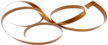


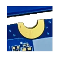
Reliable Soldering Performance
Get a solderable surface that supports component attachment during PCB assembly, helping you achieve consistent solder joints when the board design and assembly process are properly controlled.

Get custom HASL PCB solutions with dependable solderability, controlled manufacturing quality, and engineering support from prototype to production.
Why PCBMASTER
PCBMASTER provides customized HASL PCB manufacturing for projects that require dependable solderability, practical manufacturing solutions, and cost-effective production. With six self-owned factories spanning 80,000 m² and approximately 100 R&D engineers, we support diverse PCB configurations, from prototypes to volume production, with integrated PCB fabrication and PCBA assembly services.
Our engineering team reviews your HASL PCB specifications, including pad geometry, board thickness, copper weight, and layer count, to identify potential manufacturing issues before production. You can select leaded or lead-free HASL according to your assembly process, product requirements, and applicable regulations. We also provide manufacturing inspection and electrical testing based on your project specifications to verify board quality before shipment.
Supported by ISO 9001 and IATF 16949 quality management systems, PCBMASTER helps you coordinate PCB fabrication and assembly, evaluate manufacturing feasibility, and control production risks. Whether you are developing a prototype or preparing for mass production, our engineering and manufacturing support helps you select suitable HASL PCB solutions for your application and budget.
Manufacturing Capabilities
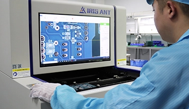
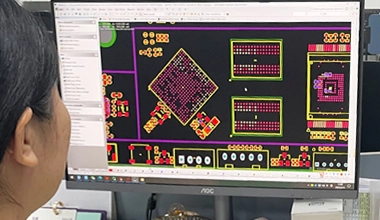
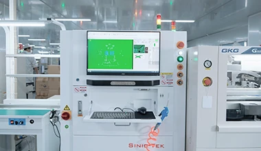
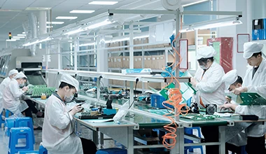
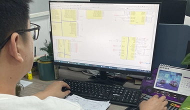
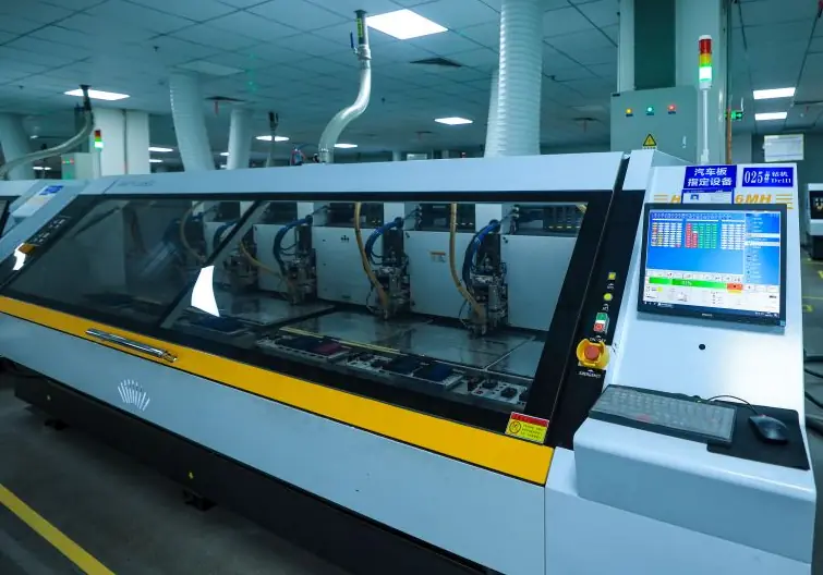
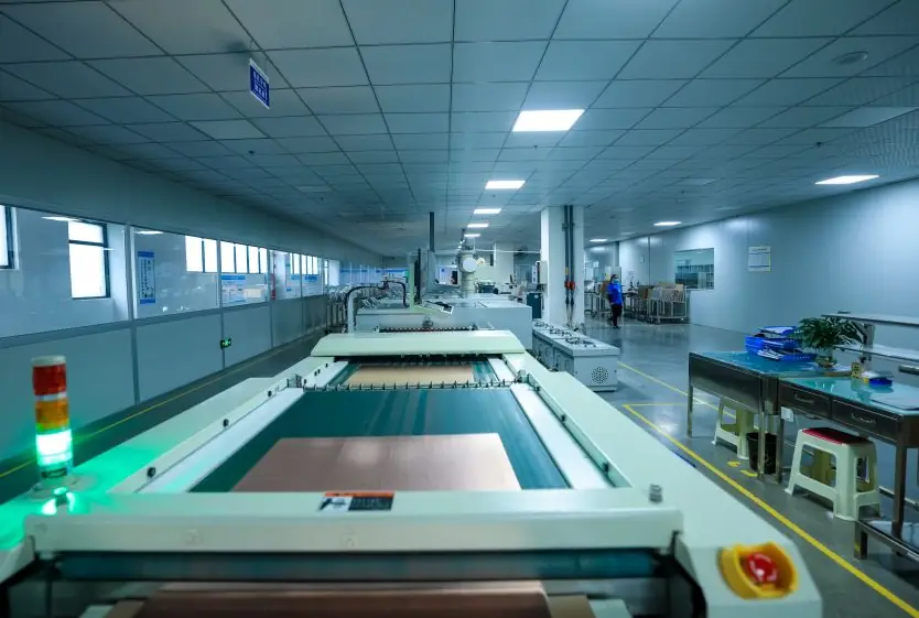
Our production lines cover the full PCB manufacturing process—from inner-layer imaging and lamination to drilling, plating, solder-leveling, surface finish, and final inspection. These facilities support the technical requirements behind HASL PCB manufacturing, including solder coating, hot-air leveling, pad-finish control, and assembly compatibility.
Product Introduction
HASL PCB, or Hot Air Solder Leveling PCB, is a printed circuit board with a solder coating applied to exposed copper pads. This surface finish protects the copper from oxidation and provides a solderable surface for component assembly. It is widely used in electronic products where reliable soldering and manufacturing cost are important considerations.
The HASL PCB manufacturing process typically includes copper pad cleaning and preparation, flux application, contact with molten solder, hot-air leveling to remove excess solder, and final inspection. Cleaning and other process steps depend on the specific production line and process requirements.
One of the main advantages of HASL PCB is its established manufacturing process and cost-effectiveness for many conventional circuit board designs. However, hot-air leveling does not produce perfectly coplanar pads. For fine-pitch components, such as certain BGA and QFN packages, ENIG or another suitable surface finish may provide better planarity.
When you choose HASL PCB from PCBMASTER, your board specifications, pad geometry, component requirements, and assembly process should be evaluated to determine whether HASL is suitable for your application.
Key Features
HASL PCB offers a practical surface finish for projects that prioritize reliable soldering, copper protection, and cost-effective manufacturing. Understanding its key characteristics helps you determine whether it fits your PCB design and assembly requirements.
Get a solderable surface that supports component attachment during PCB assembly, helping you achieve consistent solder joints when the board design and assembly process are properly controlled.
The solder coating helps protect exposed copper pads during storage and handling, supporting solderability when boards are assembled under appropriate storage conditions.
HASL is well suited to many standard PCB layouts and component packages, giving you a practical surface-finish option for general-purpose electronics. For fine-pitch components, evaluate pad planarity before selecting HASL.
For suitable designs and production volumes, HASL can help you control PCB finishing costs while meeting everyday soldering requirements. Actual cost advantages depend on board specifications, order quantity, and alternative finishes.
Product Categories
PCBMASTER provides HASL PCB options for different board structures, soldering requirements, and project stages, helping you select a suitable solution for your design and budget.
| Product Category | Description |
|---|---|
| Lead-Free HASL PCB | Choose Lead-Free HASL PCB for projects requiring a lead-free solder finish. It provides a solderable surface for component assembly and supports applicable environmental compliance requirements. |
| Leaded HASL PCB | Leaded HASL PCB uses a tin-lead solder alloy to finish exposed copper pads. It offers a practical surface finish for projects where leaded materials are permitted by regulations and customer specifications. |
| Double-Sided HASL PCB | Double-Sided HASL PCB provides copper circuitry on both sides, giving you more routing space than a single-sided board for conventional electronic designs. |
| Multilayer HASL PCB | Multilayer HASL PCB supports complex routing, power distribution, and signal interconnections within a compact footprint, making it suitable for designs that require multiple conductive layers. |
| Heavy Copper HASL PCB | Heavy Copper HASL PCB combines higher copper weight with a solderable surface finish to support power electronics and other designs requiring greater current-carrying capacity or heat spreading. |
| HASL PCB Prototype | HASL PCB Prototype lets you validate circuit layouts, component footprints, and assembly requirements before volume production, helping you identify potential issues earlier and reduce development risk. |
Applications
HASL PCB provides a solderable surface finish for electronic products across multiple industries. Its suitability depends on component pitch, assembly requirements, and operating conditions.
| Application | Description |
|---|---|
| Industrial Control | For PLCs, relay boards, and automation controllers, the HASL finish provides solderable pads for mounting control components and establishing electrical connections. |
| Consumer Electronics | In audio devices, electronic gadgets, and everyday consumer products, HASL PCB offers a practical, cost-effective surface finish for compatible component layouts. |
| Automotive Electronics | For suitable automotive control and interface boards, HASL provides a solderable surface for component assembly, subject to application-specific reliability and qualification requirements. |
| Power Electronics | In power supplies and converters, HASL-finished pads support soldering of power components when the board design meets current-carrying and thermal requirements. |
| Telecommunications | Communication control and interface boards can use HASL PCB to support the assembly of connectors and electronic components when pad geometry is compatible with the finish. |
| Home Appliances | For appliance control and power boards, the HASL finish provides solderable pads for microcontrollers, relays, and other electronic components, offering a practical option for cost-sensitive designs. |
| IoT and Sensors | In sensor interfaces, monitoring modules, and IoT controllers, HASL-finished pads support component assembly when the design does not require the tighter pad planarity of alternative finishes. |
| Computing Equipment | Peripheral boards, interface circuits, and general-purpose computing electronics can use HASL PCB where component spacing and assembly requirements are compatible with its surface characteristics. |
| Test and Measurement | For instrument control and signal interface boards, HASL provides solderable pads for assembling components used in measurement, monitoring, and test equipment. |
From prototype validation to production, PCBMASTER helps you select suitable HASL PCB specifications, review manufacturability, control quality, and coordinate PCB fabrication with assembly requirements.
Manufacturing Capabilities
PCBMASTER provides HASL PCB manufacturing for prototype, small-batch, and volume-production projects. With support for multilayer fabrication, specialty materials, and multiple surface finishes, we help you match board specifications to your design and assembly requirements.
| Specification | PCBMASTER Manufacturing Capabilities |
|---|---|
| Layer Count | 1–64 layers for supported PCB configurations. |
| Base Material | FR-4, High-Tg FR-4, halogen-free laminates, high-frequency materials, polyimide, metal core, and ceramic. |
| Board Thickness | Up to 6.0 mm for supported PCB configurations. |
| Copper Weight | Finish copper: 1–10 oz; Inner copper: 0.5–40 oz. |
| Minimum Trace Width / Spacing | 3/3 mil to 1/1 mil across supported technologies; actual limits depend on board structure, copper thickness, and process. |
| Minimum Drill Size | 0.05 mm laser-drilled holes for supported PCB configurations. |
| Solder Mask Colors | Green, black, blue, red, yellow, white, and customized options. |
| HASL Solder Alloy | Leaded HASL and Lead-Free HASL. |
| Electrical Testing and Inspection | Electrical testing, flying probe testing, and AOI inspection. |
| Quality Standards | ISO 9001, IATF 16949, UL, and RoHS. |
Case Studies
PCBMASTER has supplied HASL PCBs for customers across a wide range of industries, supporting different circuit designs, board structures, and assembly requirements.
The customer needed a cost-effective PCB for an industrial controller integrating relay circuits, control signals, and external connectors. The main challenge was providing reliable interconnections without adding unnecessary manufacturing complexity.
PCBMASTER manufactured a representative double-sided standard FR-4 PCB with a 1.6 mm board thickness and 1 oz copper. Copper circuits on both sides provided routing space, while plated through-holes connected the two layers. PCBMASTER applied a HASL finish to exposed copper pads, creating solderable surfaces for the selected component footprints. Electrical testing checked circuit continuity and isolation before shipment.
The double-sided structure provided the required circuit connections without the added complexity of a multilayer stack-up. Combined with the HASL finish, this configuration offered a practical manufacturing solution for conventional controller circuits, supporting component assembly while keeping board construction straightforward.
The customer needed a compact PCB for an automotive auxiliary control module with multiple signal connections and defined thermal requirements. The main challenge was accommodating complex routing within a restricted footprint while selecting a laminate suitable for the project’s operating conditions.
PCBMASTER manufactured a representative four-layer high-Tg FR-4 PCB with a 1.2 mm board thickness and 1 oz copper. Internal copper layers provided additional routing paths, while plated through-holes connected the required layers. The high-Tg laminate was selected as a candidate for the specified thermal requirements, and HASL was applied to exposed pads compatible with the selected component footprints.
The multilayer structure supported circuit integration within the available space, while the HASL finish provided solderable surfaces for compatible components. This configuration supported the board’s progression toward assembly and automotive qualification, subject to the project’s required validation tests.
The customer needed a PCB for a power supply carrying higher currents through designated power paths. The key challenge was controlling conductor resistance while maintaining suitable soldering surfaces for power components and connectors.
PCBMASTER manufactured a representative double-sided FR-4 PCB with a 2.0 mm board thickness and 2 oz copper. The heavier copper reduced conductor resistance compared with thinner copper of the same geometry. Trace widths and copper areas were configured around the intended current paths, while plated through-holes connected circuits across both sides. HASL provided solderable pads for compatible power components and terminals.
The combination of heavier copper and a solderable surface supported the board’s electrical and assembly requirements. It provided a practical foundation for power-supply integration, with actual current capacity and temperature rise dependent on the completed layout and operating conditions.
The customer needed a compact PCB for a consumer electronic device with limited installation space and a specified halogen-free material requirement. The challenge was accommodating the required circuit connections while balancing board thickness, routing density, and assembly cost.
PCBMASTER manufactured a representative four-layer halogen-free FR-4 PCB with a 1.0 mm board thickness and copper weights selected according to the design requirements. The multilayer stack-up provided additional routing paths within the restricted footprint, while plated through-holes connected the required conductive layers. HASL was applied to exposed pads compatible with the component packages and pad spacing, providing a practical solderable finish for the intended assembly process.
The multilayer structure supported a compact circuit layout, while the halogen-free laminate addressed the project’s specified material requirement. The HASL finish offered a cost-conscious assembly surface where its pad profile was compatible with the component design, supporting the customer’s progression toward product integration.
Customer Reviews
PCBMASTER’s HASL PCB customers value consistent board quality, practical engineering support, dependable delivery, and smooth coordination between PCB fabrication and assembly.
For us, a PCB isn't good just because it looks good in a photo. We care about the pad finish, board condition, and whether the quality stays consistent when we reorder. That's what we look at with our HASL boards from PCBMASTER. Consistency matters more to our production team than impressive promises.
 Michael Carter · Quality Manager · Industrial Automation · United States
I tend to look at the details that can cause trouble later, especially pad geometry and component spacing. HASL can be a sensible choice, but it isn't right for every footprint. I value being able to discuss those practical manufacturing considerations with PCBMASTER before a design moves into production.
 Sophie Laurent · PCB Design Engineer · Consumer Electronics · France
My biggest concern is what happens when a PCB order starts affecting the production schedule. I need clear answers on lead time, order status, and any changes that could affect delivery. For our HASL PCB orders, straightforward communication is what helps me coordinate purchasing with the production team.
 Daniel Weber · Procurement Manager · Power Electronics · Germany
I'd rather not spend my week chasing separate suppliers for the bare board and assembly. Having PCB and PCBA support available through PCBMASTER gives us a more direct way to coordinate the HASL board requirements with the assembly process. Fewer handoffs make the workflow easier for our team to manage.
 Emma Wilson · Operations Director · Industrial Electronics · United Kingdom
Learn what to consider when choosing HASL PCB, from component compatibility and storage requirements to manufacturing specifications and surface finish selection.
Choose based on your product’s regulatory requirements, soldering process, and customer specifications. Lead-free HASL uses a lead-free solder alloy and is often preferred for products subject to lead-restriction requirements. Traditional leaded HASL may remain suitable for applications where leaded materials are legally permitted. Confirm the required alloy and compliance documentation before ordering.
HASL can be suitable for many conventional surface-mount components, but it becomes less attractive as component pitch decreases. Hot-air leveling can leave variations in solder thickness across pads, affecting coplanarity and solder-joint formation. If your design includes fine-pitch QFNs, BGAs, or other components with demanding coplanarity requirements, compare HASL with flatter finishes such as ENIG before finalizing the PCB design.
It depends on the BGA pitch, ball size, pad design, and assembly process. Because BGA packages rely on an array of closely spaced solder joints, pad-height variation can complicate assembly. For fine-pitch BGAs, ENIG is often worth evaluating because of its flatter surface. Share the component datasheet and footprint with your PCB manufacturer so the finish can be assessed against the actual assembly requirements.
HASL provides a solder coating that protects exposed copper from direct oxidation, helping preserve solderability during storage. However, shelf life also depends on packaging, humidity, contamination, and storage conditions. Keep boards in their original protective packaging, avoid unnecessary handling of exposed pads, and follow the manufacturer’s storage recommendations. Confirm the applicable storage period if your project requires long-term inventory.
HASL can support mixed-technology assembly when the surface finish is compatible with the component footprints and soldering process. Through-hole components and many conventional SMT devices can use HASL-finished pads. However, closely spaced SMT pads may be more sensitive to solder-height variation. Evaluate the smallest component pitch and the assembly process together rather than assuming one finish will suit every component on the board.
HASL is not automatically unsuitable for high-frequency circuits, but it should not be selected without considering the electrical design. At higher frequencies, conductor geometry, dielectric properties, impedance control, and surface effects become increasingly important. The solder coating can also influence conductor-surface characteristics. For RF or high-speed designs, discuss the operating frequency, impedance requirements, and signal-loss budget with your PCB manufacturer before choosing HASL.
Yes, HASL may be used on suitable heavy-copper PCB designs, provided the board structure, exposed pad geometry, and finishing process are compatible. However, heavy copper introduces additional considerations for etching, plating, thermal behavior, and manufacturing uniformity. If your board carries high current, specify the copper weight and electrical requirements separately from the surface finish. HASL provides solderable pads; it does not determine the board’s current-carrying capacity.
Provide the Gerber or other accepted manufacturing data, drill files, board outline, layer stack-up, copper weights, board thickness, solder mask requirements, and the specified HASL type. Include the bill of materials and assembly drawings if you also require PCBA. State any controlled impedance, dimensional tolerance, inspection, testing, or compliance requirements explicitly. Complete documentation reduces clarification cycles and helps the manufacturer evaluate manufacturability before production.
Compare more than the unit price. Check whether each quotation specifies the same layer count, board dimensions, copper weight, board thickness, HASL alloy, tolerances, testing requirements, and order quantity. Also confirm tooling charges, panelization assumptions, lead time, packaging, and whether electrical testing is included. A lower quotation may reflect different specifications or exclusions, so evaluate the total cost against your actual manufacturing requirements.
Consider another finish when your design requires flatter pads, tighter assembly tolerances, or specific surface characteristics that HASL cannot reliably provide. ENIG is often evaluated for fine-pitch components and BGA assembly, while OSP may suit certain cost-sensitive SMT designs with controlled handling and storage. Immersion silver can be considered for selected applications with appropriate storage controls. The best option depends on component pitch, assembly method, product environment, shelf-life needs, and total project cost.
Related Products
PCBMASTER offers a range of PCB surface finishes and board configurations to meet different assembly requirements, component layouts, and application needs. Explore these related products to find the right solution for your project.
A flat, uniform surface finish suitable for fine-pitch components, BGA packages, and designs requiring consistent pad planarity.
Learn more →An organic protective coating applied to exposed copper pads, offering a cost-effective option for compatible soldering processes.
Learn more →Provides a relatively flat, solderable surface for designs where pad geometry and assembly requirements call for an alternative to HASL.
Learn more →Integrates multiple conductive layers to support more complex routing, power distribution, and signal connections in a compact board.
Learn more →Uses thicker copper conductors to support higher current requirements and manage heat when the board design is appropriately engineered.
Learn more →Combines bare PCB fabrication with component sourcing and assembly to help coordinate board specifications, soldering requirements, and production.
Learn more →Share your PCB files, board specifications, surface finish requirements, and order quantity. PCBMASTER can review your project requirements and help identify a suitable manufacturing approach.

