


Professional IC Substrate R&D and Manufacturing
Request a QuoteWhy Choose Our IC Substrate
We combine advanced technology, strict quality control and customer-centric service to deliver exceptional IC Substrate solutions.
Premium Materials
We stock substrates from leading brands including SYTECH, BT, Mitsubishi, Doushan, Toshiba, LG, Yinghua, ABF to ensure stable performance and adaptability.
Precision Manufacturing
With minimum line width/spacing of 25μm and minimum laser drilling diameter of 0.05mm,
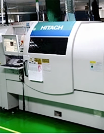
Equipped with LDI exposure machines and high-precision laser drilling.
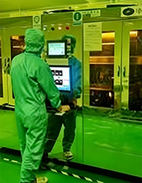
Full-process QC
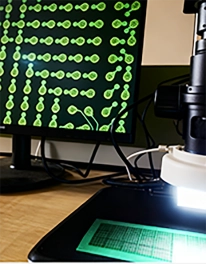
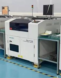
Real-time online AOI monitoring throughout the process, 100% inspection of samples with professional IC substrate micro-probe flying probe testers.
Quality Certification
Compliant with AS9100 Aerospace-Grade Quality Management Certification and ROHS environmental standards, ensuring every substrate meets industry highest requirements.
Fast Delivery
Sample lead time only 12-30 days, supporting full-process customization from PCB Prototypes to small-batch production to meet rapid iteration needs.
Expert Team
20-strong R&D team with proven track records in top-tier IC substrate R&D and production, providing one-stop service from technical consultation to customized production.
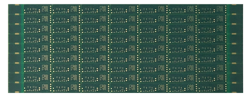
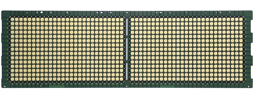
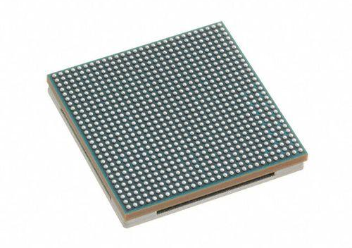
Our Products of IC Substrate
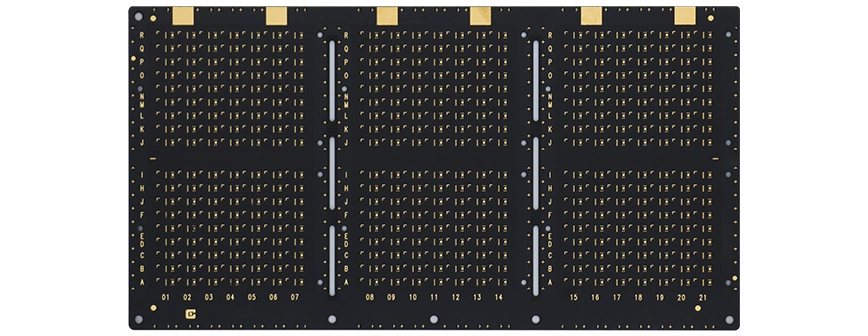
SiP Substrate
System-in-Package (SiP) is currently widely used in various portable communication electronics products.
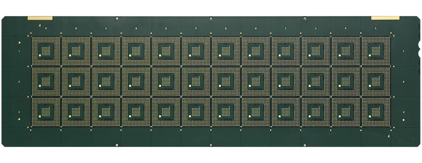
PBGA Substrate
Wire-bond plastic packaging substrates are currently widely used in the packaging of medium/low contact density electronic components such as computer and communication products.
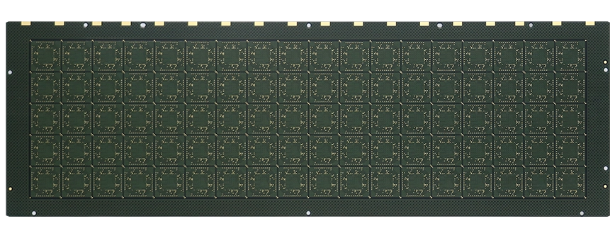
FCCSP Substrate
Widely used in the packaging of low contact density electronic components such as consumer electronics and communication devices, which emphasize lightweight, thinness, compact dimensions and compactness.
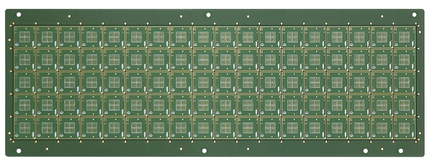
FCBGA Substrate
Flip-chip packaging substrates are currently widely used in the packaging of high-speed computing/high contact density electronic components such as computers and communication devices.
Memory Card Substrate
Memory Card Packaging Substrates (MCP Substrates) are currently widely used in various electronic products such as memory cards, computers, mobile phones, storage devices, and servers.
LGA Substrate
Land Grid Array (LGA) is primarily utilized in high-end electronic products centered on semiconductors and chips and demanding high-frequency, high-power, and high-density I/O scenarios.
| Package Type | PBGA | TBGA | CBGA | CCGA | Micro BGA |
|---|---|---|---|---|---|
| Substrate Material | BT Resin | Polyimide | Multilayer Ceramic | Multilayer Ceramic | Optional |
| Encapsulation | Over mold/Glob Top/Cap | Optional Cap | Optional Cap | Optional Cap | Over mold/Glob Top/Optional Cap |
| Package Size | 7-50mm | 21-40mm | 18-32mm | 32-42.5mm | Chip Scale |
| Die Orientation | Up/Down | Up | Up/Down | Up/Down | Up/Down |
| Interconnect | Solder Ball 63Sn/37Pb | Solder Ball 10Sn/90Pb | Solder Ball 10Sn/90Pb | Solder Column 10Sn/90Pb | Metal Ball Solder/Gold |
| Pitch | 1.0 / 1.27 / 1.5 | 1.0 / 1.27 / 1.5 | 1.0 / 1.27 / 1.5 | 1.0 / 1.27 / 1.5 | 0.8 / 0.5 |
| Area Efficiency(Chip=1) | 7.2 | 5.3 | 4.5 | 4.5 | 1-1.4 |
Product Features / Manufacturing Capabilities
Thickness & Tolerance
Board thickness 0.1~1.2mm, tolerance ±30μm
Small and dense holes
30~150μm hole diameter, hundreds to thousands of micro holes per PCS
Fine line width and spacing
min 25μm
Small pads
Minimum BGA pad diameter: 50μm
Interconnection technology
Buried, blind, and stacked via technologies
Surface treatment
Ni/Au, soft gold, hard gold, Ni/Pd/Au, etc.
Small unit size
≤150×150mm
Dimensional tolerance
min ±50 μm
|
Material
|
SYTECH, BT, Mitsubishi, Doushan, Toshiba, LG, Yinghua, Ajinomoto Buildup Film(ABF) | ||
|---|---|---|---|
| MASS Production | Samples Production | ||
| Layer | 2-10 layers | 2-12 layers | |
| Min Drilling | 50μm | 50μm | |
| Bonding Finger | Min.Pitch | 105μm | 95μm |
| Min.Width | 35μm | 35μm | |
| Circuit Line | Min.Pitch | 95μm | 25μm |
| Min.Width | 25μm | 25μm | |
| Min.Spacing | 25μm | 25μm | |
| Min.Welding ring | 80μm | 80μm | |
| Min.Thickness | 2L | 100μm | 100μm |
| 4L | 300μm | 200μm | |
| 6L | 400μm | 300μm | |
| 10L | 800μm | / | |
| 12L | 1000μm | / | |
| Line to PAD/EDGE | 100μm | 75μm | |
| Solder mask | Solder DAM | 50μm | 50μm |
| Solder PAD | 80μm | 70μm | |
| Thickness | 20+/-5μm | 20+/-5μm | |
| Flatness | 5μm | 5μm | |
| Surface Finish | Hard Gold | Ni:5-15μm Au:0.2-0.5μm | Ni:5-15μm Au:0.2-2μm |
| Soft Gold | Ni:5-15μm Au:0.3-0.8μm | Ni:5-15μm Au:0.3-2μm | |
| ENEPIG-WB | Ni:3-8μm, Pd:0.1-0.2μm Au:0.1-0.2μm | Ni:3-8μm, Pd:0.1-0.2μm Au:0.1-2μm | |
| ENEPIG-SMT | Ni:3-8μm, Pd:0.05-0.15μm Au:0.05-0.15μm | Ni:3-8μm, Pd:0.05-0.15μm Au:0.05-2μm | |
| OSP | OSP:0.1-0.3μm | OSP:0.1-0.3μm | |
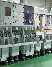
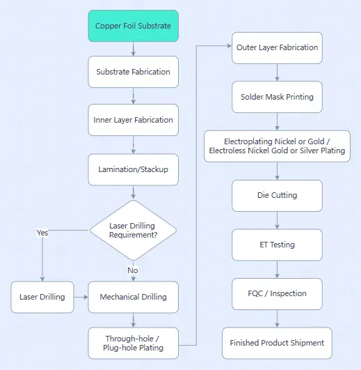
Process Flow
Blog & NEWS
-
 IC Substrate Fine Circuit Manufacturing: Techniques, Semi-Additive Process, and Ultra-Fine LinesFine circuits on IC substrates refer to the tiny copper pathways on a package board that connect different parts of an integrated circuit (IC). These circuits are responsible for transmitting signals and power between chips, ensuring the IC...May 11, 2026More
 -
How mSAP Is Used in IC Substrate Manufacturing and What to Look for in a SupplierFine-line packaging is no longer a niche requirement. Smaller form factors, higher routing density, and tighter interconnect tolerances are pushing IC substrate manufacturing far beyond the limits of conventional PCB processes. That shift i...Mar 19, 2026More
-
Tg 230℃ vs. Tg 250℃ for BT Materials in IC Substrates: Which is Better for Your Application?IC substrates are the foundation of modern electronic devices, providing crucial connections and support for integrated circuits (ICs). Without these substrates, electronic components would lack the structural integrity necessary for proper...Jan 23, 2026More
-
IC Packaging Substrate Technology for Engineers: A Comprehensive GuideIn the wave of upgrades towards higher density and miniaturization in the electronics industry, the performance of integrated circuits (ICs) relies heavily on the support of the packaging process. As a critical interface between the bare ch...Jan 15, 2026More
Technical Challenges
Ultra-thin core board processing control technology
Ultra-thin core boards are prone to warpage and expansion/contraction issues. Breakthroughs are required in process technologies such as deformation/expansion-contraction control, lamination structure design, board expansion-contraction management, lamination parameters optimization, and interlayer alignment systems. This ensures effective control of warpage and lamination thickness for ultra-thin core boards.
Micro via processing technology
Including laser drilling capability for micro blind vias, mechanical drilling capability for micro through vias, via filling technology, and stacked via technology.
Ultra-fine circuit fabrication technology
Including copper reduction capability, circuit compensation control, plating uniformity control, and etching uniformity control.
Interlayer alignment technology
Including multi-layer lamination technology, LDI (Laser Direct Imaging) alignment exposure technology, and positioning reference technology.
Solder mask fabrication technology
Including solder mask plugging (for blind vias and through vias), solder mask alignment accuracy, and solder mask flatness.
Surface finish technology
Including electroplated soft thick gold, electroplated hard thick gold, and electroless nickel palladium gold (ENEPIG), with requirements for pad flatness and fine-grained crystallization.
Testing and inspection technology
Testing of micro bonding pads requires the support of high-precision AOI (Automatic Optical Inspection) equipment and micro-probe flying probe testers for continuity testing. Meanwhile, an AOI repair process must be established to avoid quality issues caused by micro-defects.
Have any questions? PCBMASTER's technical team is ready to help.

