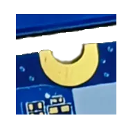
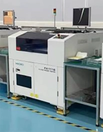
✓High-Density Routing with Microvias and Fine-Line Technology
✓Custom HDI Stack-Up and Layer Count for Your Design
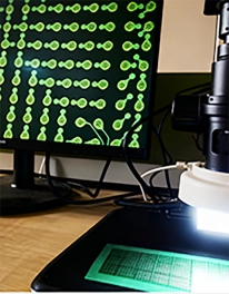
✓Reliable PCB Manufacturing with Precision Quality Control
✓Engineering Support for DFM, Via Structures, and Layout Optimization
Why PCBMASTER
Why Choose PCBMASTER for HDI Multilayer PCB Manufacturing?
When you choose PCBMASTER for HDI Multilayer PCB manufacturing, you gain access to advanced microvia technology, precision fabrication, and engineering expertise. We support laser-drilled microvias, blind vias, and buried vias to help you achieve higher routing density and integrate complex circuits into compact board designs.
Our engineering team customizes HDI Multilayer PCB stack-ups based on your component layout, routing density, signal integrity requirements, and board thickness. With fine-line fabrication capabilities, we help you accommodate high-pin-count ICs, BGA, and CSP components while optimizing interconnection structures for your specific design.
Quality is integrated throughout our HDI Multilayer PCB manufacturing process. PCBMASTER operates under ISO 9001 and IATF 16949 quality management systems, holds UL certification, and provides RoHS-compliant PCB solutions. These quality and compliance measures help you meet product requirements while maintaining consistent manufacturing quality and reliability.
From DFM analysis and microvia structure review to stack-up optimization, our engineers provide technical support to help you reduce design risks and improve manufacturability. Whether you need HDI PCB prototypes, small-batch production, or volume manufacturing, PCBMASTER offers flexible production solutions to meet your project requirements.
ISO 9001
IATF 16949
UL
RoHS
Product Introduction
What Is an HDI Multilayer PCB and How Does It Improve Your Design?
An HDI Multilayer PCB (High-Density Interconnect Multilayer Printed Circuit Board) is a specialized circuit board that uses advanced interconnection technologies, such as microvias, blind vias, buried vias, and fine-line circuitry, to achieve higher wiring density across multiple conductive layers. Unlike conventional Multilayer PCB designs that primarily rely on mechanical through-holes, HDI PCB technology provides more flexible interconnection structures for complex electronic layouts.
When you need to integrate high-pin-count components such as BGA, CSP, and advanced processors into a limited board area, an HDI Multilayer PCB offers greater routing flexibility and component density. Shorter interconnection paths can also help reduce parasitic inductance and capacitance, supporting improved electrical performance in high-speed applications. These advantages make HDI PCB technology particularly suitable for compact electronic products with demanding design requirements.
At PCBMASTER, your HDI Multilayer PCB is manufactured according to your Gerber files, stack-up specifications, material requirements, and application needs. Our manufacturing process accommodates different HDI structures and design configurations, allowing you to select a suitable solution for your project. From initial engineering review to fabrication and quality verification, we help you translate complex PCB designs into manufacturable circuit boards while addressing design-specific requirements.
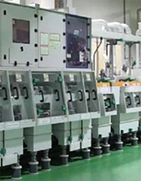
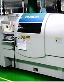
PCBMASTER operates an integrated production base covering laser drilling, sequential lamination, fine-line imaging, and comprehensive inspection. Our controlled manufacturing environment and quality procedures help ensure consistent HDI Multilayer PCB quality from prototype development to volume production.
Key Features
Key Features of HDI Multilayer PCB Technology
HDI Multilayer PCB technology combines microvia interconnections, fine-line circuitry, and multilayer construction to meet your high-density design requirements. These features give you greater routing flexibility, support advanced component integration, and help you develop compact electronic products without compromising circuit complexity.
Feature
Description
High Interconnection Density
Fit more electrical connections into limited board space, giving you greater layout flexibility for compact designs.
Microvia Technology
Connect selected conductive layers with small-diameter vias, helping you optimize routing space around densely packed components.
Fine-Line Circuitry
Accommodate narrow traces and tight spacing to simplify routing between fine-pitch components and high-density pads.
Multilayer Construction
Distribute complex circuits across multiple conductive layers, allowing you to integrate more functions within a single PCB.
High-Density Component Compatibility
Support fine-pitch BGA, CSP, and advanced IC packages, helping you meet demanding component integration requirements.
Flexible Interconnection Structures
Choose blind, buried, stacked, or staggered microvia configurations to better match your routing needs and board architecture.
Product Solutions
Explore Our HDI Multilayer PCB Solutions
With a diverse range of HDI Multilayer PCB solutions, PCBMASTER helps you find the right interconnection structure for your design complexity, component density, and routing requirements. From standard build-up configurations to advanced microvia architectures, you can choose a solution that fits your board layout, space constraints, and performance goals.
Product Category
Description
1+N+1 HDI Multilayer PCB
Achieve efficient high-density routing with a single build-up layer on each side of the core, ideal for compact designs with moderate interconnection complexity.
2+N+2 HDI Multilayer PCB
Accommodate denser component layouts and more complex routing with two build-up layers on each side of the core.
3+N+3 HDI Multilayer PCB
Handle demanding interconnection requirements with multiple build-up layers, giving you greater routing flexibility for advanced electronic designs.
Any-Layer HDI PCB
Connect any required conductive layers through microvias, helping you overcome routing constraints in highly dense and space-limited designs.
High-Layer-Count HDI PCB
Integrate complex circuits across numerous conductive layers to support advanced electronic systems with demanding interconnection requirements.
Blind and Buried Via HDI PCB
Optimize internal routing space by connecting selected layers without occupying all layers with through-holes.
Stacked Microvia HDI PCB
Build vertical interconnections across multiple layers to support dense component fan-out and compact, complex circuit layouts.
Staggered Microvia HDI PCB
Use offset microvia connections across sequential layers to achieve flexible routing arrangements for your HDI design.
PCBMASTER provides HDI Multilayer PCB solutions for a wide range of industries, including consumer electronics, automotive, medical, telecommunications, and industrial automation. By combining high-density interconnections, microvia technology, and multilayer circuit structures, our HDI PCBs help you overcome routing limitations, integrate complex electronic components, and achieve more compact designs across diverse applications.
Application
Description
Smartphones
Enable dense BGA routing and integrate processors, memory, cameras, and wireless modules in slim devices.
Wearable Electronics
Minimize PCB footprints while connecting miniature sensors, wireless chips, and power management components.
Medical Electronics
Integrate imaging processors, diagnostic sensors, and precision control circuits within compact medical devices.
Automotive Electronics
Accommodate high-pin-count processors and complex connections in compact ADAS and electronic control modules.
Telecommunications Equipment
Support dense, high-speed signal routing between communication processors, RF modules, and networking components.
Aerospace Electronics
Reduce circuit board size and weight while accommodating complex avionics and communication systems.
Industrial Automation
Integrate control processors, sensor interfaces, and communication circuits into space-constrained industrial equipment.
Consumer Electronics
Combine multiple functional circuits within smaller boards for compact, multifunctional electronic products.
Computing and Server Systems
Enable dense processor and memory interconnections while supporting complex multilayer routing architectures.
Your HDI Multilayer PCB Partner for Precision, Reliability, and Design Flexibility.
PCBMASTER combines advanced HDI fabrication, engineering expertise, and rigorous quality control to support your demanding electronic design requirements.
HDI Multilayer PCB Solutions for Real-World Applications
PCBMASTER delivers HDI Multilayer PCB solutions for diverse projects across multiple industries, including consumer electronics, automotive, medical equipment, and high-speed networking. Explore how our engineering expertise and advanced manufacturing capabilities address complex design challenges and meet demanding application requirements.
01
Compact Smartphone HDI PCB
A smartphone manufacturer approached PCBMASTER to develop a compact HDI multilayer PCB for a new-generation smartphone. The board needed to integrate an application processor, high-speed memory, multiple camera modules, and wireless communication components within a restricted installation area. The main challenges included fine-pitch component routing, limited via placement space, and maintaining reliable connections across multiple layers.
PCBMASTER developed a 12-layer HDI PCB using a 3+N+3 sequential build-up structure. Laser-drilled microvias with a 0.075 mm finished diameter, 0.075 mm minimum line width and spacing, and optimized stacked and staggered via arrangements provided additional routing channels. The engineering team also optimized the stack-up and reference planes to support high-speed signal transmission. Precision laser drilling, sequential lamination, and AOI inspection were applied during production.
The solution enabled the customer to integrate more functional components into a smaller PCB footprint while maintaining reliable interconnections and supporting the smartphone's compact design requirements.
02
Automotive ADAS HDI Multilayer PCB
An automotive electronics supplier required an HDI multilayer PCB for an ADAS control unit integrating radar processing, camera interfaces, and vehicle communication circuits. The project required high-density interconnections, controlled impedance for high-speed signals, and stable electrical performance under automotive operating conditions. Maintaining microvia reliability and layer-to-layer registration also presented manufacturing challenges.
PCBMASTER designed a 10-layer HDI PCB with a 2+N+2 build-up structure, 0.10 mm laser microvias, and 0.075 mm minimum line width and spacing. Controlled-impedance routing, dedicated ground reference planes, and optimized power distribution were incorporated into the stack-up. Sequential lamination, precision copper plating, and automated optical inspection helped maintain interlayer connection quality. Electrical testing, impedance verification, and thermal reliability evaluations were included in the quality control process.
The solution provided the customer with a compact, high-density circuit platform for ADAS electronics, supporting reliable signal transmission and the integration of multiple vehicle sensing and processing functions.
03
Medical Imaging HDI PCB
A medical equipment manufacturer needed a high-density PCB for an advanced ultrasound imaging system. The board had to connect multiple signal-processing channels, imaging processors, memory devices, and control circuits within a limited enclosure. The key challenges involved routing numerous sensitive signals, reducing interference between analog and digital circuits, and maintaining consistent interconnection quality.
PCBMASTER developed a 14-layer HDI multilayer PCB with a 3+N+3 build-up structure. A 0.075 mm minimum laser microvia diameter and 0.075 mm line width and spacing provided the routing density required by the design. The stack-up incorporated dedicated ground and power planes to improve signal isolation and power distribution. Precision sequential lamination, laser drilling, copper plating, and AOI inspection were used to control manufacturing quality. Electrical continuity, insulation resistance, and microsection inspections supported process verification.
The finished PCB helped the customer integrate complex imaging electronics into a smaller assembly while providing the interconnection density and electrical stability required for medical imaging signal processing.
04
High-Speed Networking HDI PCB
A networking equipment manufacturer approached PCBMASTER for an HDI multilayer PCB used in a high-speed Ethernet switch. The design needed to connect switching ASICs, high-speed memory, optical transceiver interfaces, and power management circuits. Its primary challenges were dense BGA fan-out routing, strict impedance requirements, and minimizing signal interference across multiple high-speed channels.
PCBMASTER engineered a 16-layer HDI PCB with a 3+N+3 sequential build-up structure. Laser-drilled microvias, a 0.075 mm minimum line width and spacing, and optimized BGA fan-out routing helped accommodate the dense component connections. The stack-up was designed with controlled-impedance signal layers and continuous reference planes. PCBMASTER also applied precision lamination, laser drilling, copper plating, and impedance testing to maintain dimensional and electrical consistency throughout production.
The solution provided the customer with a high-density interconnection platform for high-speed networking hardware, supporting complex signal routing, efficient component integration, and stable electrical performance.
What Engineers and Buyers Say About PCBMASTER HDI Multilayer PCB Solutions
PCBMASTER’s multilayer HDI PCB solutions have earned positive feedback from customers across various industries. Explore how our engineering expertise, manufacturing quality, and project support address the needs of engineers and buyers.
Hardware Design Engineer – Consumer Electronics
★★★★★
The routing density was a major concern for our compact electronics design. PCBMASTER helped us work through the HDI multilayer PCB requirements, particularly the microvia structure and fine-line routing. Their engineering team was responsive when we needed to clarify design details, which made the development process much smoother.
Michael Chen | Hardware Design Engineer | Consumer Electronics | United StatesProcurement Manager – Automotive Electronics
★★★★★
From a procurement perspective, consistency matters just as much as pricing. PCBMASTER has demonstrated good attention to manufacturing quality and production coordination for our HDI multilayer PCB orders. Communication regarding production progress has also been helpful, allowing us to manage our sourcing schedule with greater confidence.
Thomas Weber | Procurement Manager | Automotive Electronics | GermanyR&D Engineer – Medical Devices
★★★★★
The multilayer HDI PCB for our medical device project required dense interconnections and precise integration of fine-pitch components. What I appreciated most was the technical discussion with PCBMASTER’s engineers. They understood our design constraints and helped address several manufacturing concerns before production. Their engineering support was valuable throughout our product development process.
Sarah Mitchell | R&D Engineer | Medical Devices | United StatesProject Manager – Telecommunications
★★★★★
Managing a multilayer HDI PCB project involves more than meeting specifications. We need clear communication, coordinated production, and dependable technical support. PCBMASTER maintained good communication throughout the project and helped us keep the manufacturing process aligned with our requirements. This made project coordination considerably easier for our team.
James Anderson | Project Manager | Telecommunications | United Kingdom
The right HDI Multilayer PCB structure depends on component pitch, routing density, signal speed, board dimensions, and manufacturing budget. A 1+N+1 structure may be sufficient for moderate routing complexity, while 2+N+2 or 3+N+3 structures provide additional routing capacity for more demanding designs. Evaluate the actual fan-out requirements before selecting a more complex build-up structure.
These structures indicate the number of sequential build-up layers on each side of the core. 1+N+1 uses one build-up layer on each side of the core and is suitable for moderate interconnection density. 2+N+2 uses two build-up layers on each side to support more complex component fan-out. 3+N+3 uses three build-up layers on each side to accommodate highly dense routing and advanced component integration. The value of N represents the number of core layers, and the appropriate structure depends on routing feasibility, cost, and reliability requirements.
Material selection should consider dielectric constant (Dk), dissipation factor (Df), thermal performance, moisture resistance, and dimensional stability. Standard FR-4 materials are suitable for many general-purpose HDI designs. High-speed or high-frequency applications may require low-loss materials to reduce signal attenuation. For fine-pitch components and sequential lamination, stable dimensional characteristics are also important.
No. Low-loss materials are primarily necessary when signal frequency, data rate, or transmission distance makes dielectric loss a significant concern. Many control circuits, embedded systems, and moderate-speed digital applications can use conventional FR-4 materials. Selecting unnecessarily expensive materials may increase project costs without providing meaningful performance improvements.
Copper thickness influences current-carrying capacity, resistance, heat generation, and fine-line fabrication. Thicker copper can support higher current loads, but it may make fine-line etching more difficult and increase routing constraints. Engineers should balance copper thickness with trace width, operating current, temperature rise, and the minimum line spacing required by the design.
Stacked microvias are vertically aligned across multiple layers, allowing compact interconnections within limited PCB space. Staggered microvias are offset from one another, providing an alternative routing arrangement that can reduce certain interconnection reliability risks. Stacked structures may require additional process control and copper filling. The choice should consider routing density, fabrication capability, and long-term reliability requirements.
Cost optimization starts with simplifying the design where possible. Consider reducing unnecessary build-up layers, minimizing stacked microvias, optimizing panel utilization, and selecting materials that meet rather than exceed electrical requirements. Standardizing board thickness and copper specifications may also improve manufacturing efficiency. Early design-for-manufacturability (DFM) reviews can identify expensive design features before production begins.
To obtain an accurate quotation, prepare the following information: Gerber or ODB++ fabrication data, NC drill files for mechanical and laser-drilled vias, PCB stack-up specification, board dimensions and layer count, copper thickness and material requirements, minimum line width and spacing, surface finish requirements, controlled impedance specifications if applicable, and required quantity and delivery schedule. Providing complete manufacturing data helps the supplier evaluate fabrication complexity and identify potential technical issues.
Do not evaluate a manufacturer solely by its advertised minimum line width or microvia diameter. Review its actual production capabilities, including sequential lamination, laser drilling, microvia copper filling, fine-line fabrication, and layer registration control. Ask for relevant cross-section reports, electrical test records, impedance verification data, and examples of comparable HDI projects. These records provide a more meaningful basis for assessing manufacturing capability.
Before releasing an order, confirm that the final manufacturing specifications match your design requirements. Pay particular attention to the approved stack-up, material grade, finished board thickness, copper weight, via structure, surface finish, impedance tolerances, and inspection criteria. You should also clarify the production lead time, quantity, packaging requirements, and acceptance standards. A documented engineering review helps reduce specification misunderstandings and prevents avoidable production delays.
Have more questions? Our technical team is ready to help.
Explore PCBMASTER’s related PCB technologies to find the right solution for your design requirements, component density, electrical performance, and product development goals.
We use necessary cookies to ensure basic site functionality (browsing, quotation, login) and optional analytics cookies to optimize our service.
Your data is strictly confidential and will never be sold or shared with any third party.
Your consent is voluntary and revocable.
We use necessary cookies to ensure basic site func...