Microvia PCB

Custom Microvia PCB Manufacturing for High-Density Designs

Build compact, high-density electronics with Microvia PCB solutions engineered around your stack-up, routing density, and manufacturing requirements.

  • 1 Precision Laser-Drilled Microvias for High-Density Routing
  • 2 Custom HDI Stack-Up Design for Complex Multilayer PCBs
  • 3 DFM Review and Engineering Support from Prototype to Production
  • 4 Quality-Controlled Manufacturing and Pre-Shipment Testing

Why PCBMASTER

Why Choose PCBMASTER for Microvia PCB Manufacturing?

PCBMASTER provides Microvia PCB manufacturing solutions tailored to your high-density interconnect requirements, from microvia structure selection and HDI stack-up design to fabrication and quality inspection. Our engineering team helps you evaluate laser-drilled microvias, stacked and staggered structures, via-in-pad designs, and layer-to-layer connections to improve routing efficiency and manufacturing feasibility.

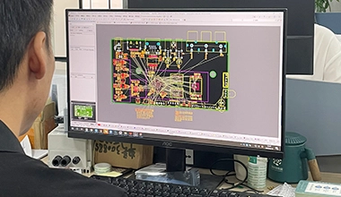
With experience across diverse PCB technologies, PCBMASTER supports custom Microvia PCB projects requiring precise interconnections, complex multilayer structures, and consistent manufacturing quality. Our engineering team reviews your design specifications and manufacturing files to identify potential issues before production, helping reduce avoidable design revisions and fabrication risks.

Quality assurance is central to every Microvia PCB project. PCBMASTER operates under ISO 9001 and IATF 16949 quality management systems and holds UL certification and RoHS compliance certification. Pre-shipment testing helps verify that finished boards meet applicable electrical and manufacturing requirements. In addition, our stable material supply and supply chain management help support material availability, consistent manufacturing quality, and reliable production planning from prototypes to volume manufacturing.

Manufacturing Capabilities

Inside Our PCB Manufacturing Facilities

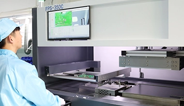
Our production lines cover the full PCB manufacturing process—from inner-layer imaging and laser drilling to lamination, plating, microvia formation, surface finish, and final inspection. These facilities support the technical requirements behind Microvia PCB manufacturing, including precision laser drilling, sequential lamination, microvia filling, and high-density interconnection verification.

PCB manufacturing facility 1
PCB manufacturing facility 2
PCB manufacturing facility 3
PCB manufacturing facility 4
PCB manufacturing facility 5
PCB manufacturing facility 6
PCB manufacturing facility 7
PCB manufacturing facility 8

Product Introduction

What Is a Microvia PCB and How Does It Support High-Density Interconnects?

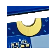
A Microvia PCB uses small-diameter vias to connect conductive layers within a printed circuit board, making it possible to achieve higher routing density without increasing the overall board footprint. Unlike conventional through-holes that pass through multiple layers, microvias typically connect adjacent layers, preserving valuable routing space on inner layers. This structure is particularly useful for fine-pitch BGA and CSP packages, where conventional fan-out routing may be difficult to implement.

When selecting a Microvia PCB, you should consider more than the via diameter. The aspect ratio, pad dimensions, dielectric thickness, copper distribution, and via arrangement all influence manufacturability and long-term reliability. Stacked microvias provide vertical connections across multiple layers, while staggered microvias use offset connections. The appropriate structure depends on your routing constraints, electrical requirements, and fabrication capabilities.

Before requesting a quote from PCBMASTER, prepare your manufacturing files, layer stack-up, board dimensions, copper thickness, microvia specifications, surface finish, order quantity, and required lead time. Providing these details helps PCBMASTER evaluate manufacturing feasibility, identify potential design constraints, and prepare an accurate quotation for your Microvia PCB project.

Key Features

Key Features of Microvia PCB Technology

Microvia PCBs feature compact interlayer connections and fine-pitch structures that help you optimize routing density and reduce board size.

Feature Description
Small Via Diameter Fit more interconnections into limited board space with smaller-diameter vias.
Shallow Via Depth Connect conductive layers through thin dielectric sections to support compact HDI stack-ups.
Short Interlayer Span Preserve inner-layer routing space by connecting adjacent layers without traversing the full board thickness.
Laser-Drilled Openings Achieve precise, small-diameter via openings for fine-pitch component interconnections.
Small Capture Pads Free up more routing area around vias to accommodate dense circuit layouts.
Thin Dielectric Layers Arrange conductive layers closer together to support compact, high-density circuit designs.

Product Categories

Explore Microvia PCB Types for Your Design Requirements

PCBMASTER offers the following Microvia PCB types to meet your design requirements, from basic HDI interconnections to complex multilayer structures, helping you select the right solution for your routing density and layout constraints.

Product Category Description
Single-Level Microvia PCB Connects adjacent conductive layers through one microvia level, giving you a straightforward HDI structure for compact circuit layouts.
Stacked Microvia PCB Aligns microvias vertically across multiple layers, helping you achieve dense interconnections within limited board space.
Staggered Microvia PCB Offsets microvias between layers, providing alternative routing paths for complex multilayer designs.
Via-in-Pad Microvia PCB Places filled and capped microvias directly within component pads, helping you route fine-pitch BGA connections where conventional fan-out is difficult.
Any-Layer HDI Microvia PCB Supports microvia connections between adjacent layers throughout the stack-up, giving you greater routing flexibility for highly integrated designs.
High-Layer-Count Microvia PCB Combines microvia interconnections with numerous conductive layers, helping you accommodate complex routing requirements within a compact board footprint.

Build Better HDI Designs with Microvia PCB Manufacturing Expertise.

From engineering review and prototype fabrication to production support, PCBMASTER helps you evaluate microvia structures, optimize manufacturing readiness, and align PCB fabrication with your project requirements.

Applications

Microvia PCB Solutions for Advanced Electronic Applications

PCBMASTER provides Microvia PCB solutions for electronic applications that require compact layouts, high-density interconnections, and efficient component routing.

Application How Microvia PCBs Are Used
Smartphones Connect fine-pitch application processors, memory chips, and RF components to inner PCB layers, enabling dense BGA fan-out and compact motherboard layouts.
Wearable Devices Route signals between miniature processors, sensors, memory, and wireless chips through closely spaced layers, helping fit more functions into small wearable circuit boards.
Medical Electronics Provide dense interconnections for imaging sensors, signal-processing ICs, and wireless modules, allowing portable diagnostic and patient-monitoring devices to accommodate complex circuitry within limited board space.
Automotive Electronics Fan out fine-pitch processors and control ICs in ADAS modules, electronic control units, and infotainment systems, enabling dense signal routing within compact automotive circuit boards.
Networking Equipment Connect high-pin-count switching ASICs, network processors, and high-speed interface ICs to inner routing layers, helping manage dense signal connections while preserving space for impedance-controlled routing.
Computing and Servers Route connections from high-density CPU, GPU, memory, and accelerator packages into multilayer PCB structures, supporting fine-pitch BGA escape routing and complex interconnections in computing hardware.
IoT Devices Connect compact microcontrollers, wireless communication chips, sensors, and power-management ICs across multiple PCB layers, reducing routing congestion in space-constrained connected devices.
Industrial Automation Provide compact interconnections for controllers, communication processors, sensor interfaces, and other fine-pitch components, helping integrate control and monitoring functions into space-limited industrial electronics.
Aerospace Electronics Route dense connections from high-pin-count processors, navigation ICs, and communication components into multilayer circuit boards, helping reduce board footprint in compact avionics and mission-specific electronic systems.

Case Studies

Microvia PCB Engineering Solutions for Real-World Design Challenges

PCBMASTER has helped customers across multiple industries solve real-world Microvia PCB design and manufacturing challenges.

01

How Microvia PCB Design Supports Compact Consumer Electronics

8-Layer HDI0.10 mm MicroviaConsumer

A handheld consumer electronics project required a compact PCB integrating a BGA processor, memory, and wireless communication components. Routing signals from the processor’s fine-pitch pads proved difficult because conventional via placement consumed valuable inner-layer routing space. Increasing the board dimensions was not an option due to the existing enclosure constraints.

To resolve the routing congestion, PCBMASTER’s engineering team redesigned the BGA escape region and adopted an 8-layer HDI stack-up with 0.10 mm laser-drilled microvias connecting adjacent conductive layers. Via locations were coordinated with the BGA pad arrangement and inner-layer routing channels, allowing selected signals to transition between layers without relying exclusively on full-thickness through-holes.

The revised layout accommodated the required interconnections within the planned board outline. Manufacturing documentation also specified microvia geometry, layer registration, and electrical continuity requirements, providing a clearer basis for prototype fabrication and design verification.

02

Microvia PCB Solutions for Space-Constrained Automotive Electronics

10-Layer HDI0.10 mm MicroviaAutomotive

Within a compact automotive control module, a microcontroller, power-management circuitry, sensor interfaces, and communication connections had to fit into a restricted installation space. The primary challenge was organizing dense interconnections while maintaining the customer’s specified manufacturing tolerances and reliability requirements.

PCBMASTER developed a 10-layer HDI layout using 0.10 mm laser-drilled microvias for adjacent-layer connections. The engineering review addressed dielectric thickness, copper distribution, via placement, and layer registration. These parameters were coordinated with the component layout to reduce unnecessary routing detours and account for fabrication constraints.

As a result, the design established routing paths for the control and communication circuits within the intended PCB outline. The manufacturing documentation defined dimensional inspection, electrical testing, and traceability requirements to support production verification against the customer’s specifications.

03

HDI Microvia PCB Manufacturing for Dense Communication Hardware

12-Layer HDI50 ΩNetworking

Dense connections between high-speed interface components and signal-processing circuits created routing congestion in a communication hardware project. Conventional via placement restricted available routing channels, while the design required controlled impedance and appropriate reference-plane continuity.

PCBMASTER reorganized the signal-layer assignments and microvia locations within a 12-layer HDI stack-up. The design specified 0.10 mm laser-drilled microvias for designated layer transitions and a nominal 50 Ω impedance target for applicable single-ended signals. Trace geometry was coordinated with dielectric properties, copper thickness, and the complete stack-up to meet the specified electrical design requirements.

Through this revised routing arrangement, the manufacturing files established clearer requirements for interlayer connections and impedance-controlled traces. Electrical and dimensional inspection criteria were also documented so the finished boards could be evaluated against the project’s specified requirements.

04

Custom Microvia PCB for Compact Medical Electronics

8-Layer HDI0.10 mm MicroviaMedical

For a portable diagnostic electronics design, the customer needed to integrate sensor inputs, processing circuitry, memory, and communication interfaces within a limited enclosure. The restricted PCB area made component placement and conventional routing difficult, particularly where several functional circuits required connections across multiple layers.

PCBMASTER developed an 8-layer HDI layout incorporating 0.10 mm laser-drilled microvias between adjacent conductive layers. The design coordinated via placement with the sensor interfaces and processing circuits while accounting for dielectric thickness, capture-pad geometry, copper distribution, and surface-finish requirements. Dimensional tolerances and electrical test criteria were incorporated into the manufacturing documentation.

The resulting layout defined a routing structure for the compact circuit and established clear fabrication requirements for production. Dimensional inspection and electrical continuity testing provided the basis for checking the finished PCB against the specified requirements, with acceptance determined by the customer’s documented criteria.

Customer Reviews

What Customers Value in Microvia PCB Manufacturing

Customers from different industries choose PCBMASTER for their Microvia PCB projects, and many value our responsive engineering support, consistent manufacturing quality, and reliable communication throughout the process.

Engineering Support
The biggest headache was routing the BGA without making the board any larger. We had already tried a few layout options, but the escape routing was still too crowded. PCBMASTER went through the Microvia PCB design with us and suggested a more practical via arrangement. I especially appreciated that their engineers explained why certain options would or wouldn't work in manufacturing. It saved us from going back and forth on designs that weren't feasible.
Michael Turner · Senior Hardware Engineer · Consumer Electronics · United States Michael Turner · Senior Hardware Engineer · Consumer Electronics · United States
Manufacturing Quality
When we source Microvia PCBs for automotive applications, we can't rely on a supplier's general promise of good quality. We need clear specifications, proper inspection, and traceability. What mattered to us was how PCBMASTER handled the details and responded to our quality requirements. Their team was willing to discuss the checks needed for our boards rather than treating the order as just another production run.
Daniel Fischer · Supplier Quality Manager · Automotive Electronics · Germany Daniel Fischer · Supplier Quality Manager · Automotive Electronics · Germany
Communication and Delivery
I'm usually juggling several things at once, so the last thing I need is to keep chasing a supplier for updates. During our Microvia PCB project, communication with PCBMASTER was straightforward. When we asked about production progress or delivery timing, we could get the information needed to plan our next steps. Things don't always go exactly as planned in hardware projects, but clear communication makes a real difference.
Sophie Laurent · Project Manager · Communication Equipment · France Sophie Laurent · Project Manager · Communication Equipment · France
Production Partnership
Getting the prototype made is only the first step. What I really look at is whether a supplier can support us when the design moves toward repeat production. With PCBMASTER, we were able to discuss Microvia PCB manufacturing requirements early, rather than leaving every production question until the next order. From a sourcing perspective, that kind of forward planning is valuable because it helps us manage changes and prepare for future demand.
Oliver Bennett · Strategic Sourcing Manager · Medical Electronics · United Kingdom Oliver Bennett · Strategic Sourcing Manager · Medical Electronics · United Kingdom
12 FAQ

More About Microvia PCB

Before choosing a Microvia PCB, it’s worth understanding how it affects your design, manufacturing costs, and long-term reliability. Here are answers to common questions to help you make an informed decision.

FAQ · 01

How Do I Know If My Design Needs a Microvia PCB?

A Microvia PCB is worth considering when fine-pitch components, such as BGAs with tight ball spacing, leave insufficient room for conventional via structures and escape routing. Review your component pitch, available routing channels, board dimensions, and layer count. If conventional vias force you to increase the board size or add unnecessary layers, microvias may provide a more efficient interconnection strategy.

FAQ · 02

What Is the Difference Between a Microvia PCB and a Conventional Multilayer PCB?

The main difference is the interlayer connection structure. Conventional multilayer PCBs commonly use plated through-holes that extend through the entire board, while Microvia PCBs use small, typically laser-drilled vias to connect adjacent or nearby conductive layers. This allows routing resources to be used more efficiently, particularly in high-density layouts. A Microvia PCB can still include conventional through-holes or buried vias where the design requires them.

FAQ · 03

Does a Microvia PCB Always Reduce the Total Board Cost?

No. Microvias can reduce board area or help avoid additional layers, but laser drilling, sequential lamination, via filling, and specialized inspection may increase fabrication costs. The overall cost depends on whether these processes offset savings from a smaller footprint, improved panel utilization, or a simpler routing structure. Compare complete manufacturing quotations rather than evaluating the cost per via alone.

FAQ · 04

How Does Microvia Diameter Affect PCB Design?

A smaller microvia can free up routing space, but reducing its diameter also places greater demands on laser drilling, copper plating, registration, and inspection. The appropriate diameter depends on the dielectric thickness, target aspect ratio, capture-pad dimensions, and the fabricator’s demonstrated process capability. Specify a diameter based on actual routing needs rather than choosing the smallest available feature by default.

FAQ · 05

Are Stacked Microvias More Reliable Than Staggered Microvias?

Neither structure is universally more reliable. Stacked microvias align vertically across successive layers and can provide a compact interconnection path, but they place greater demands on interlayer registration, copper filling, and interface integrity. Staggered microvias use offset connections and can reduce some of the structural demands associated with directly stacked interfaces, although they require more lateral space. Reliability depends on the complete structure, materials, fabrication process, and qualification results.

FAQ · 06

What Causes Microvia PCB Failures During Thermal Cycling?

Potential failure mechanisms include separation at copper interfaces, cracks in the microvia barrel or target pad, and weaknesses associated with dielectric materials or inadequate copper deposition. Repeated temperature changes can create mechanical stress because different PCB materials expand at different rates. Appropriate material selection, controlled plating and lamination processes, sound microvia geometry, and thermal-cycle testing help evaluate reliability for the intended operating environment.

FAQ · 07

Can Microvias Be Used Directly Under BGA Pads?

Yes. A via-in-pad structure can place a microvia within a component pad, allowing dense BGA connections to be routed into inner layers with less fan-out space. However, the process typically requires the via to be filled and capped to create a suitable surface for component mounting and soldering. Confirm the filling method, surface planarity, pad geometry, and assembly requirements with the PCB manufacturer before finalizing the layout.

FAQ · 08

How Many Layers Should a Microvia PCB Have?

There is no fixed layer count for a Microvia PCB. The appropriate number depends on signal routing density, power distribution, grounding, impedance requirements, component placement, and board dimensions. A higher layer count may simplify routing in some designs, but it can also increase material and lamination costs. Stack-up planning should begin with the electrical and mechanical requirements, then be refined through routing analysis and manufacturability review.

FAQ · 09

Which PCB Materials Are Suitable for Microvia PCB Manufacturing?

FR-4 is suitable for many Microvia PCB applications, particularly where standard electrical and thermal performance is sufficient. High-speed, high-frequency, or high-temperature designs may require materials with more specific dielectric, loss, or thermal properties. Material selection should also account for coefficient of thermal expansion, glass-transition temperature, moisture behavior, and compatibility with sequential lamination and microvia fabrication processes.

FAQ · 10

How Can I Verify the Reliability of a Microvia PCB Supplier?

Ask the supplier about its laser-drilling limits, supported microvia structures, sequential lamination process, via-filling capabilities, and inspection methods. Request relevant fabrication specifications, cross-section inspection results, electrical test procedures, and reliability qualification data where applicable. It is also useful to establish how the supplier handles process deviations and whether its manufacturing controls are suitable for your required production volume and application.

FAQ · 11

What Files and Specifications Should I Provide for a Microvia PCB Quote?

Prepare the Gerber or ODB++ manufacturing data, drill files, layer stack-up, board dimensions, copper thickness, and surface-finish requirements. Clearly identify microvia diameters, layer-to-layer connections, stacked or staggered structures, via-in-pad requirements, and any controlled-impedance specifications. Include order quantity, prototype or production requirements, target lead time, and applicable acceptance criteria. Complete information helps the manufacturer assess feasibility and quote more accurately.

FAQ · 12

When Should I Choose a Microvia PCB Manufacturer for Prototype and Mass Production Together?

Consider using the same manufacturer when your project requires a smooth transition from initial prototypes to repeat production. The manufacturer should be able to review the design early, confirm the feasibility of the microvia structure, document critical process parameters, and explain how prototype findings will be incorporated into production controls. This approach can reduce avoidable redesigns and help maintain consistency as order volumes increase. Before committing, confirm capacity, qualification requirements, production lead times, and the process for approving engineering changes.


Ready to Start Your Microvia PCB Project?

Share your Microvia PCB design requirements with PCBMASTER to evaluate manufacturing feasibility, review your HDI stack-up, and request a project-specific quotation.

Home Quote Order
Get Coupon