Heavy Copper PCB Manufacturer for High-Current and High-Power Applications
Get custom Heavy Copper PCBs designed to handle demanding electrical loads, manage heat effectively, and support reliable operation in high-power electronic systems.
✓0.25–20 oz Copper Weight Options for Custom Designs
✓Precision Heavy Copper PCB Fabrication
✓Optimized Electrical and Thermal Performance
✓ISO 9001 & IATF 16949 Certified Manufacturing
Por qué PCBMASTER
Why Choose PCBMASTER for Heavy Copper PCB Manufacturing?
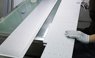
PCBMASTER supports copper weights ranging from 0.25 oz to 20 oz, giving you flexible options for different current-carrying, power distribution, and thermal management requirements. From prototype quantities to volume production, we manufacture Heavy Copper PCBs tailored to your electrical and structural specifications.
We maintain a stable supply of quality copper-clad laminates and prepregs from reliable material manufacturers. Careful material selection based on your operating temperature, electrical requirements, and PCB structure helps ensure consistent substrate quality and production stability.
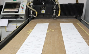
Heavy copper fabrication requires precise control over circuit patterning and etching. PCBMASTER optimizes etching parameters to manage trace width, spacing, and lateral etching, helping maintain circuit accuracy and dimensional consistency across different copper thicknesses.
Our lamination process focuses on controlling temperature, pressure, and resin flow to achieve proper resin filling around thick copper features and reliable interlayer bonding. These factors are particularly important for multilayer Heavy Copper PCBs with complex copper distributions.
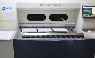
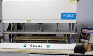
Quality assurance is integrated throughout production. We use AOI, electrical testing, copper thickness inspection, and final quality checks to verify critical product requirements before shipment. Our ISO 9001 and IATF 16949 quality management systems support standardized manufacturing and consistent quality control.
From initial design review and DFM analysis to prototype fabrication and volume production, our engineering team helps you address manufacturing challenges, optimize PCB structures, and achieve reliable production outcomes.
ISO 9001
IATF 16949
EN _ RU
Suscribirse
Introducción del producto
What Is a Heavy Copper PCB and How Does It Support High-Power Circuit Designs?
A Heavy Copper PCB is a printed circuit board manufactured with significantly thicker copper layers than conventional PCBs. While standard PCBs commonly use 1–2 oz copper, Heavy Copper PCBs generally use 3 oz or more, although the exact threshold varies among manufacturers and industry definitions. The increased copper thickness provides greater conductor cross-sectional area, making these boards suitable for demanding power applications.
Compared with standard PCBs, Heavy Copper PCBs can carry higher currents within appropriately designed circuits, reduce conductor resistance, and improve heat spreading. Their thicker copper traces also support more robust circuit structures, allowing designers to integrate power and control circuits while addressing demanding electrical and thermal requirements.
The working principle is based on the relationship between copper cross-sectional area, electrical resistance, and current capacity. Increasing copper thickness reduces conductor resistance for a given trace width and length, which helps limit resistive losses and associated heat generation. The additional copper also provides a more effective path for distributing heat across the board.
4-Layer Heavy Copper PCB Cross-Section — 6 oz Copper
At PCBMASTER, each Heavy Copper PCB project begins with reviewing your design files and electrical requirements. Our engineering team evaluates the proposed circuit structure, copper distribution, and manufacturing considerations before proceeding with fabrication, inspection, and delivery. This approach helps you address overheating risks, insufficient current capacity, and power density limitations while developing reliable high-power electronic products.
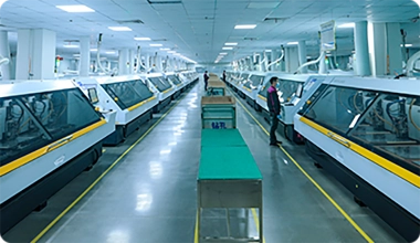
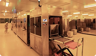
PCBMASTER operates an integrated production base covering heavy copper etching, multi-layer lamination under controlled pressure and temperature, AOI inspection, and 100% electrical testing. Our controlled manufacturing environment and quality procedures help ensure consistent Heavy Copper PCB quality from prototype development to volume production.
Características principales
Heavy Copper PCB Features
Heavy Copper PCBs feature thicker copper layers and conductors, providing greater design flexibility for high-current and power-intensive applications.
Característica
Descripcion
Increased Copper Thickness
Provides thicker copper layers to meet demanding current-carrying and thermal requirements.
Greater Copper Cross-Section
Offers a larger conductive area to support higher current capacity and reduce conductor resistance.
Higher Copper Content per Unit Area
Provides more copper material for current conduction and heat spreading across the board.
Thicker Circuit Traces
Creates thicker conductive paths to accommodate demanding power distribution requirements.
Soluciones de productos
Explore Our Heavy Copper PCB Solutions for Different Power Requirements
PCBMASTER offers a variety of Heavy Copper PCB configurations to accommodate different circuit designs, power requirements, and installation constraints, helping you find the right solution for your application.
Tipo de producto
Descripcion
Single-Sided Heavy Copper PCB
Features heavy copper circuitry on one side, providing a straightforward and cost-effective solution for high-current power distribution.
Double-Sided Heavy Copper PCB
Features copper circuitry on both sides, offering greater routing flexibility and supporting more compact power circuit designs.
Multilayer Heavy Copper PCB
Integrates multiple conductive layers to accommodate complex circuit layouts and distribute high currents within limited board space.
Rigid-Flex Heavy Copper PCB
Combines rigid and flexible circuit sections, enabling space-efficient layouts and reliable connections in compact or complex assemblies.
Heavy Copper PCB Applications Across High-Power Industries
Heavy Copper PCBs provide reliable high-current conduction and improved heat dissipation, supporting power transmission, energy conversion, and electrical control across a wide range of industries.
APLICACIÓN
Heavy Copper PCB Function
Electric Vehicles
Carries high currents in traction inverters, motor controllers, and battery power distribution circuits.
EV Charging Stations
Handles high charging currents in power conversion modules and charging output circuits.
Energías Renovables
Transfers high currents in solar inverters, wind power converters, and energy storage systems.
Industrial Power Supplies
Provides low-resistance conductive paths for rectification, switching, and high-power DC output circuits.
Motor Drives
Carries high currents between power switching devices and motor output connections.
Battery Management Systems
Provides robust current paths for battery charging, discharging, and protection circuits.
Welding Equipment
Carries high welding currents in power conversion and welding output control circuits.
Power Distribution Systems
Distributes high currents between power input terminals, busbar connections, and output circuits.
Telecommunications Power Systems
Supports high-current power distribution between rectifier modules, DC buses, and backup battery systems.
Your Reliable Heavy Copper PCB Manufacturing Partner
From stable material supply and precision fabrication to comprehensive testing and dedicated engineering support, PCBMASTER helps you move heavy copper PCB projects from prototype to production with confidence.
Heavy Copper PCB Solutions for Real-World Industrial Applications
PCBMASTER’s Heavy Copper PCBs support a wide range of industrial projects, from electric vehicle power distribution to renewable energy, motor drives, and battery energy storage. Explore how our engineering solutions address different project requirements across these industries.
01
EV Power Distribution PCB
An automotive electronics manufacturer approached PCBMASTER for a heavy copper PCB used in an electric vehicle power distribution unit. The board needed to distribute current between the battery pack, traction inverter, and auxiliary power circuits. The project required reliable high-current conduction, controlled temperature rise, and stable electrical insulation within a compact installation space.
The main challenge was accommodating high-current power paths without increasing the board footprint. PCBMASTER's engineering team selected a 6-layer heavy copper structure with 4 oz copper on the primary power layers and 2 oz copper on the signal and control layers. The finished board measured 2.0 mm in thickness, with optimized power trace widths of 8–12 mm according to individual circuit current requirements. The design also incorporated wider copper areas to improve heat spreading and reduce conductor resistance.
After fabrication, the boards underwent electrical continuity, insulation resistance, and thermal performance testing. The optimized copper distribution provided reliable power transmission, helped control localized heating, and supported stable operation of the vehicle's power distribution system.
02
Solar Inverter Heavy Copper PCB
A solar inverter manufacturer required a heavy copper PCB for a 50 kW three-phase solar inverter. The board was used in the inverter's power conversion stage, where high switching currents and continuous operation placed considerable demands on copper conductivity and thermal management. The customer needed a PCB capable of supporting high-power operation while maintaining consistent electrical performance.
The primary challenge was managing current concentration and heat generation around the power switching devices. PCBMASTER developed a 4-layer PCB with 4 oz copper on the power layers and 2 oz copper on the remaining layers. The finished board thickness was 2.4 mm, with power traces designed at widths of 6–10 mm. The engineering team optimized the copper layout around the switching devices and DC bus connections to provide larger conductive cross-sections and more effective heat spreading.
Following fabrication, the boards underwent 100% electrical testing, copper thickness inspection, and thermal verification under the specified operating conditions. The heavy copper design provided lower-resistance power paths and improved thermal distribution, helping the inverter maintain reliable DC-to-AC power conversion.
03
Industrial Motor Drive PCB
An industrial automation equipment manufacturer needed a heavy copper PCB for a 30 kW variable-frequency motor drive. The PCB carried current through the inverter's switching stage and motor output circuits. The customer required a robust board design capable of handling frequent load changes, high switching currents, and extended operating periods.
The engineering challenge involved balancing current-carrying capacity, heat dissipation, and insulation spacing within the available board dimensions. PCBMASTER designed a 6-layer PCB with 3 oz copper on the main power layers and 2 oz copper on the other layers. The board had a finished thickness of 2.0 mm, while the main power traces were designed with widths of 5–10 mm. Copper distribution and component placement were optimized to reduce localized heating around high-current switching paths.
The finished boards passed electrical continuity, insulation resistance, and thermal performance checks. The reinforced power paths helped reduce resistive losses and manage heat generation, providing stable electrical connections for motor control during demanding industrial operation.
04
Battery Energy Storage PCB
An energy storage equipment manufacturer approached PCBMASTER for a heavy copper PCB used in a battery energy storage system. The board connected battery modules to the main power distribution circuit and carried charging and discharging currents. The customer required low-resistance connections, effective heat management, and sufficient electrical clearance to support continuous energy transfer.
The main challenge was accommodating multiple high-current connections within a limited PCB area while maintaining consistent current distribution. PCBMASTER developed a 4-layer heavy copper PCB with 5 oz copper on the main power layers and 2 oz copper on the signal layers. The finished board thickness was 2.0 mm, with main battery power traces measuring 10–15 mm in width. The engineering team optimized the copper layout around battery terminals and power distribution connections to increase conductive cross-sectional area and improve heat spreading.
After fabrication, the boards underwent 100% electrical testing, copper thickness inspection, and insulation testing. The heavy copper construction provided robust battery current paths, reduced conductor resistance, and helped manage heat during charging and discharging operations.
What Our Customers Say About PCBMASTER’s Heavy Copper PCB
Trusted by customers across different industries, PCBMASTER’s Heavy Copper PCBs are recognized for their consistent quality, reliable manufacturing capabilities, responsive engineering support, and dependable delivery. Here’s what our customers say about working with us.
Consistent Copper Thickness Makes a Difference in Power Applications
★★★★★
With heavy copper boards, copper thickness consistency is something we pay close attention to. Even small variations can affect current-carrying performance and heat distribution in our application. We evaluated the boards against our specified copper weights and dimensional requirements, and the results were satisfactory. What stood out to us was the consistency across the production panels. That's particularly important when these boards are going into high-current equipment.
Michael Turner | Position: Senior Hardware Engineer | Industrial Power Electronics | United StatesTheir Engineering Feedback Helped Us Rethink the Copper Design
★★★★★
We originally planned to use a heavier copper weight throughout the board because we wanted additional current-handling capacity. During the design review, PCBMASTER's engineers pointed out that some areas could be optimized without compromising our electrical requirements. We discussed trace width, copper distribution, and manufacturing limitations before finalizing the design. I appreciated that the conversation wasn't just about whether the board could be manufactured, but also whether our original design made sense.
Daniel Weber | Electrical Design Manager | Renewable Energy | GermanyNot Every Fabricator Is Equipped for This Kind of Board
★★★★★
The challenging part of our project wasn't simply increasing the copper weight. We had several areas with thick copper features and relatively demanding dimensional requirements, which made fabrication more complicated than a standard PCB. We were concerned about whether the manufacturer could handle these details consistently. PCBMASTER worked through the manufacturing requirements with us, and the finished boards met our agreed specifications. From a manufacturing perspective, that was the result we needed.
James Mitchell | Manufacturing Engineering Director | Automotive Electronics | United KingdomGood Production Planning Starts With a Reliable PCB Supplier
★★★★★
Honestly, my biggest concern is rarely just the PCB itself. If materials arrive late or production schedules keep changing, the entire assembly plan can be affected. For our heavy copper PCB orders, we needed better visibility into material availability and production progress. PCBMASTER kept us updated during the order process, which helped us coordinate our purchasing and production schedules. That kind of communication makes a real difference when you're managing multiple orders.
Thomas Schneider | Procurement Manager | Energy Storage Systems | Netherlands
Start by evaluating the maximum operating current, allowable temperature rise, trace width, available routing space, and operating environment. Higher current requirements may call for heavier copper, but increasing copper weight alone does not guarantee better performance. You should also consider conductor geometry, thermal management, and PCB layout constraints. Working with your PCB manufacturer during the design stage can help identify a suitable copper weight.
In some applications, Heavy Copper PCBs can replace conventional busbars or integrate their functions into a more compact assembly. They can combine current distribution, component mounting, and control circuitry on a single board. However, the decision depends on current capacity, voltage, thermal dissipation, mechanical loading, and connection requirements. For very high currents, busbars may still be necessary or may work alongside the PCB.
A Heavy Copper PCB uses thicker copper layers integrated into a printed circuit board, allowing electrical routing and component mounting within the same structure. A thick copper busbar is primarily designed for high-current power distribution and generally uses solid copper conductors rather than etched PCB circuitry. Heavy Copper PCBs offer greater circuit integration, while busbars are often better suited to applications requiring very high current capacity.
Yes. Heavy copper fabrication introduces additional design considerations compared with standard PCB manufacturing. Copper etching compensation, minimum spacing, trace geometry, copper distribution, and finished conductor dimensions all need careful evaluation. Thick copper can also affect fine-pitch routing and the available space between adjacent features. It is advisable to have your PCB layout reviewed for manufacturability before finalizing the design.
Yes. Heavy Copper PCBs can be manufactured in multilayer configurations, allowing power distribution, signal routing, and ground structures to be integrated into one board. However, multilayer heavy copper designs require careful consideration of layer alignment, dielectric thickness, resin flow, lamination pressure, and thermal expansion. The achievable structure depends on copper weight, layer count, board thickness, and the manufacturer’s process capabilities.
FR-4 is commonly used for Heavy Copper PCBs because of its electrical insulation, mechanical strength, and broad availability. For applications involving elevated operating temperatures or demanding thermal conditions, high-Tg FR-4 or other specialized laminates may be more appropriate. Metal-core substrates can also be considered when heat dissipation is a major design priority. Material selection should account for operating temperature, dielectric properties, thermal requirements, and reliability expectations.
Heavy copper can influence several aspects of PCB assembly, particularly thermal behavior during soldering. Thick copper areas have greater thermal mass and can absorb more heat, potentially affecting solder joint formation and temperature uniformity. Large copper planes and heavy copper traces may also create uneven heating across the board. Assembly profiles, pad design, component placement, and soldering parameters should therefore be evaluated together with the PCB construction.
It can be designed for applications involving repeated temperature changes and mechanical stress, but reliability depends on the complete PCB construction. Copper thickness, substrate properties, copper distribution, via design, and laminate selection all influence performance. For demanding environments, thermal cycling, solder joint reliability, and interconnection testing should be considered during product validation. Appropriate design margins are essential for long-term operation.
To receive an accurate quotation, prepare the following information: Gerber files covering PCB copper layers, solder mask, silkscreen, and board outline; copper weight, meaning the required copper thickness for each layer, preferably in oz or µm; stack-up details including layer count, dielectric materials, and finished board thickness; board specifications such as dimensions, minimum trace width and spacing, hole sizes, and via requirements; surface finish such as ENIG, HASL, OSP, or another specified finish; quantity requirements covering prototype, small-batch, or volume production; and application details including operating current, voltage, temperature range, and relevant environmental conditions. Providing complete technical information helps manufacturers evaluate feasibility, identify potential DFM issues, and prepare more accurate quotations.
Beyond the quoted price, evaluate whether the manufacturer has the actual process capabilities to meet your design requirements. Important factors include: copper weight capability, meaning whether the manufacturer can reliably produce your specified copper thickness; fabrication experience with heavy copper etching, multilayer lamination, and complex board structures; quality control procedures for copper thickness, dimensions, electrical performance, and finished board quality; material supply with stable access to suitable copper-clad laminates and consistent substrate materials; engineering support to review stack-ups, trace geometry, and manufacturing feasibility before production; and production capacity to support your prototype schedule and future volume requirements. A capable manufacturer should be able to explain potential manufacturing limitations, recommend practical design adjustments, and demonstrate how its quality management processes support consistent production.
¿Tiene más preguntas? Nuestro equipo técnico está listo para ayudarle.
Depending on your electrical requirements, thermal conditions, and installation environment, different PCB structures may offer better performance for your project. Explore PCBMASTER’s related PCB solutions to find the right balance of electrical performance, thermal management, mechanical strength, and design flexibility.
Thick Copper PCB
Designed for applications requiring high current-carrying capacity and improved heat distribution, Thick Copper PCB helps support demanding power circuits. It is a suitable choice for power converters, industrial control systems, and high-current electronic equipment.
Get a Custom Heavy Copper PCB Quote from PCBMASTER
Share your copper weight, layer count, board dimensions, and application requirements. Our engineering team will review your specifications, assess manufacturing feasibility, and recommend a suitable solution for your project.
Utilizamos cookies necesarias para garantizar la funcionalidad básica del sitio (navegación, cotización, inicio de sesión) y cookies analíticas opcionales para optimizar nuestro servicio.
Sus datos son estrictamente confidenciales y nunca serán vendidos o compartidos con terceros.
Su consentimiento es voluntario y revocable.
Utilizamos cookies necesarias para garantizar la f...