Custom RF Microwave PCBs for Demanding High-Frequency Designs
Get RF Microwave PCBs engineered for low signal loss, precise impedance control, and stable electrical performance. PCBMASTER combines advanced material capabilities, precision fabrication, and dedicated engineering support to bring your high-frequency designs into production.
✓Low-Loss Substrates for High-Frequency Signal Integrity
✓Precision Impedance Control for Reliable RF Performance
✓Advanced PCB Structures with Custom Stack-Ups and Copper Thickness
✓Expert Engineering Support from Material Selection to Production
Why Choose PCBMASTER for Your RF Microwave PCB Projects?
When you choose PCBMASTER for your RF Microwave PCB projects, you gain access to high-frequency material expertise. We support specialized laminates such as Rogers, Taconic, and PTFE to meet your specific frequency, dielectric, and signal loss requirements.
Our controlled impedance engineering and custom RF PCB stack-up design help you achieve reliable signal transmission. We optimize transmission line structures, dielectric thickness, copper thickness, and layer configurations according to your electrical performance and design specifications.
With precision RF Microwave PCB fabrication, we focus on fine-line circuitry, dimensional accuracy, and consistent manufacturing quality. Our engineering team evaluates your design requirements to ensure manufacturability and alignment with your high-frequency circuit needs.
PCBMASTER operates under ISO 9001 and IATF 16949 quality management systems, with UL certification and RoHS compliance capabilities. From Gerber file review and material selection to DFM analysis and fabrication, our engineering support helps you address design challenges and achieve dependable RF Microwave PCB manufacturing results.
ISO 9001
IATF 16949
Impressum
RoHs
Produkteinführung
What Is RF Microwave PCB
An RF Microwave PCB is a specialized printed circuit board designed to transmit and process radio frequency and microwave signals with minimal signal loss and reliable electrical performance. It is widely used in communication systems, radar equipment, satellite electronics, and wireless devices where signal integrity and frequency-dependent behavior are critical. Unlike conventional FR-4 Leiterplatten , RF Microwave PCBs use specialized dielectric materials with carefully characterized dielectric constants (Dk) and dissipation factors (Df) to support high-frequency operation and predictable signal propagation.
At PCBMASTER, you can customize your RF Microwave PCB based on operating frequency, signal loss budget, circuit configuration, and environmental requirements. Whether your design involves single-layer circuits, multilayer structures, or hybrid constructions, material and structural specifications can be tailored to your application. We support prototype development, small-batch production, and volume manufacturing to accommodate different project stages. Through design review, manufacturing process verification, and quality inspection, we help you transition from initial circuit development to production-ready RF Microwave PCBs that meet your technical and application requirements.
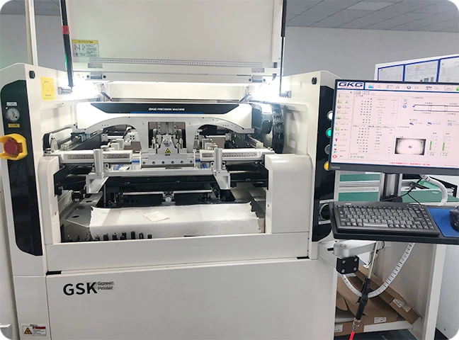
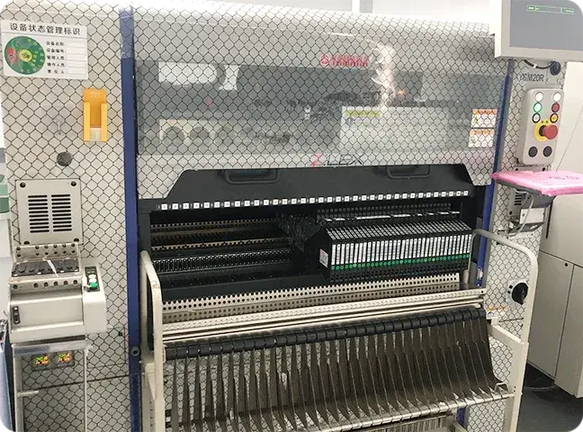
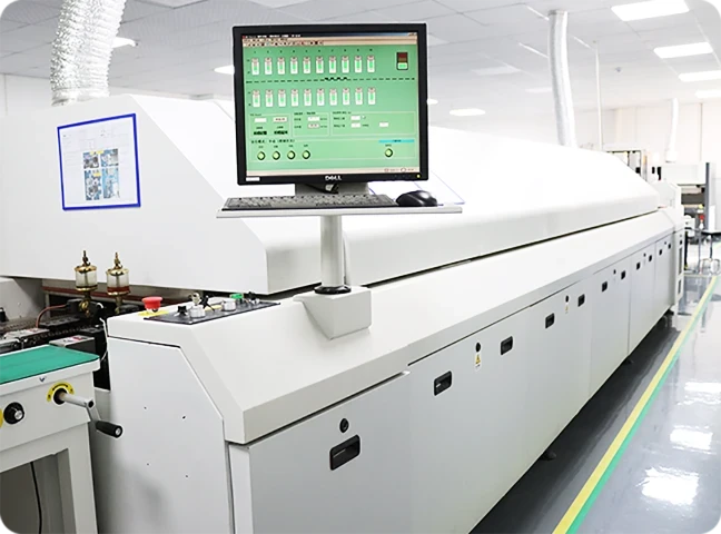
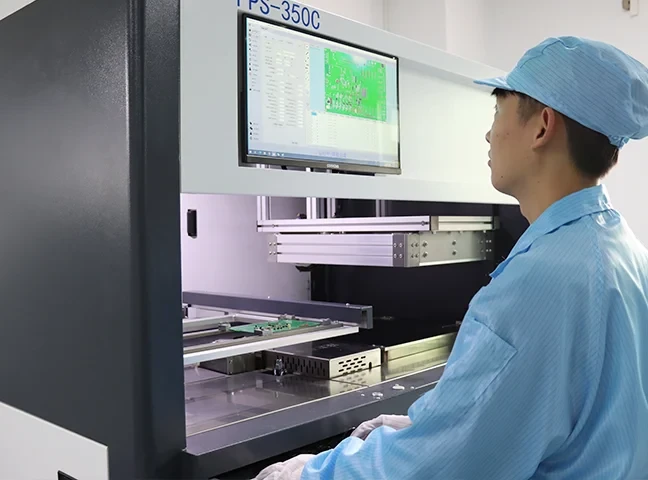
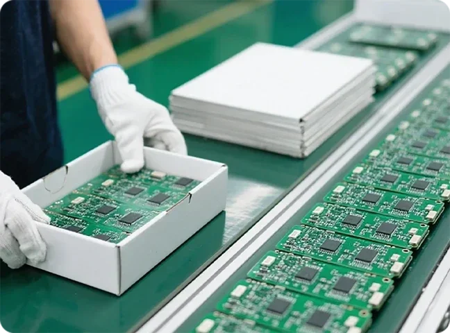
PCBMASTER operates an integrated production base covering material handling, precision imaging, lamination, and comprehensive inspection. Our controlled manufacturing environment and quality procedures help ensure consistent RF Microwave PCB quality from prototype development to volume production.
Hauptmerkmale
Key RF Microwave PCB Features for High-Frequency Circuit Design
RF Microwave PCBs use specialized dielectric materials and electrical structures to support high-frequency signal transmission. Their material properties help you reduce signal loss, maintain predictable electrical performance, and improve circuit reliability in demanding RF and microwave applications.
Feature
Description
Low Dielectric Loss
Reduces signal energy dissipation, helping you preserve signal strength during high-frequency transmission.
Stable Dielectric Constant
Provides predictable signal propagation, helping you maintain consistent circuit performance across operating frequencies.
Low Signal Attenuation
Minimizes signal degradation along transmission paths, supporting reliable communication and efficient signal delivery.
High-Frequency Electrical Performance
Supports RF and microwave circuit operation, helping you achieve dependable performance in demanding wireless applications.
Thermische Stabilität
Helps maintain electrical properties under temperature variations, reducing performance fluctuations during operation.
Dimensional Stability
Resists dimensional changes during temperature variations, helping you maintain precise circuit geometry and consistent electrical performance.
Produktlösungen
Explore Our Custom RF Microwave PCB Types
PCBMASTER offers a wide range of RF Microwave PCB solutions to accommodate different electrical, structural, and application requirements. From low-loss dielectric materials to multilayer and high-power configurations, our product options help you select the right PCB structure for your operating frequency, signal performance, and circuit integration needs.
Produkt Kategorie
Description
Rogers RF Microwave PCB
Delivers low-loss signal transmission and stable dielectric performance for demanding high-frequency communication circuits.
PTFE RF Microwave PCB
Helps minimize dielectric loss, supporting reliable signal transmission in microwave, radar, and RF applications.
Taconic RF Microwave PCB
Provides tailored dielectric properties to help you achieve consistent electrical performance across specific frequency ranges.
Hybrid RF Microwave PCB
Combines high-frequency laminates with FR-4 to balance signal performance, design flexibility, and manufacturing cost.
Multilayer RF Microwave PCB
Integrates multiple signal and ground layers, helping you achieve compact layouts and efficient circuit routing.
Ceramic-Filled RF Microwave PCB
Offers tailored dielectric and thermal properties to support demanding high-frequency circuit performance.
Antenna RF Microwave PCB
Supports optimized antenna feed networks and RF structures to improve wireless signal transmission and integration.
High-Power RF Microwave PCB
Accommodates high-power RF circuits through suitable material selection and copper configurations for improved thermal management.
RF Microwave PCB Applications Across High-Frequency Industries
RF Microwave PCBs support high-frequency signal transmission and processing across industries such as telecommunications, automotive, aerospace, satellite communication, and radar systems.
Application
Description
5G Kommunikation
Routes and distributes high-frequency RF signals between transceivers and antenna arrays, supporting signal transmission in 5G communication systems.
Radarsysteme
Connects RF transmitters, receivers, and antenna arrays, enabling the transmission and reception of radar signals for target detection.
Satellitenkommunikation
Provides low-loss transmission paths for microwave signals in satellite transceivers, frequency converters, and communication modules.
Luft- und Raumfahrt Elektronik
Integrates RF signal routing circuits in airborne communication and navigation systems, supporting reliable high-frequency signal transmission.
Wireless Infrastructure
Interconnects RF filters, amplifiers, and antenna modules to route and process signals in wireless base stations.
Microwave Test Equipment
Establishes controlled-impedance signal paths between test components, helping maintain signal integrity during high-frequency measurements.
Kfz-Radar
Connects radar transceiver circuits with antenna elements to transmit and receive high-frequency signals for vehicle detection and distance measurement.
RF Power Amplifiers
Provides impedance-matched interconnections between RF amplification stages, helping transfer high-frequency power while minimizing signal loss.
IoT Wireless Devices
Integrates RF transceiver and antenna circuits to enable wireless signal transmission and reception in compact connected devices.
Precision RF Microwave PCB Fabrication for Reliable High-Frequency Performance
Bring your RF and microwave designs closer to production with PCBMASTER. From selecting low-loss laminates and optimizing stack-ups to achieving precise impedance control, we help you address critical manufacturing challenges and maintain consistent PCB quality from prototype validation to volume production.
PCBMASTER supports diverse RF Microwave PCB projects across 5G communication, automotive radar, satellite communication, and RF power amplification. Our engineering experience covers high-frequency material selection, impedance control, stack-up optimization, and precision fabrication to address specific project requirements.
01
5G RF Communication PCB – Multilayer Rogers PCB Fabrication
A 5G communication equipment manufacturer approached PCBMASTER to develop a multilayer RF Microwave PCB for its base station RF front-end module. The board needed to support 3.5 GHz signal transmission with 50 Ω characteristic impedance while maintaining low insertion loss across multiple RF signal paths. The customer also required a compact stack-up to accommodate RF components, power distribution, and grounding structures within limited installation space.
The main challenge was controlling impedance consistency across different transmission line sections while integrating high-frequency signal layers into a multilayer structure. PCBMASTER used Rogers RO4350B laminate for the high-frequency circuit layers, with an FR-4 core for the supporting circuit structure. The engineering team optimized the dielectric thickness and copper trace width based on the target impedance and stack-up configuration. A multilayer hybrid construction was used to balance RF performance and overall board cost.
During fabrication, we controlled critical line geometries, copper thickness, and layer registration. Impedance verification and electrical inspections were performed to check compliance with the approved design requirements. The finished PCB provided the customer with integrated RF signal routing and grounding structures for its 5G base station module.
An automotive electronics manufacturer required a microwave PCB for a 77 GHz automotive radar module used in ADAS applications. The PCB needed to connect the radar transceiver IC with the antenna array while maintaining precise transmission line geometry and stable dielectric properties. At this frequency, even small variations in conductor dimensions or dielectric characteristics can affect phase response, impedance matching, and signal transmission performance.
PCBMASTER selected Rogers RO3003 high-frequency laminate as the proposed material for the radar circuit. The engineering team focused on dielectric thickness, copper surface characteristics, and transmission line geometry to meet the customer's RF design requirements. We also reviewed the antenna feed structure and ground reference configuration to reduce unwanted signal coupling.
During manufacturing, particular attention was given to fine-line imaging, drilling accuracy, and dimensional consistency. The board underwent dimensional inspection and electrical verification according to the project specifications. This manufacturing approach provided a suitable circuit platform for integrating the 77 GHz radar transceiver and antenna structures.
03
Satellite Microwave Communication PCB – Low-Loss Material Selection
A satellite communication equipment developer needed a custom microwave PCB for an X-band communication module operating around 8–12 GHz. The design required low dielectric loss, stable electrical properties, and controlled impedance to maintain signal quality throughout the transmission path. The multilayer structure also needed to accommodate RF signal routing, grounding, and supporting control circuits.
PCBMASTER selected Rogers RT/duroid 5880 PTFE laminate for the high-frequency signal layers. This material has a typical dielectric constant of 2.20 and a dissipation factor of approximately 0.0009 at 10 GHz, based on manufacturer-published data. These properties make it suitable for low-loss microwave circuit applications.
Our engineering team evaluated the dielectric thickness, copper configuration, and transmission line geometry to meet the specified impedance requirements. The manufacturing process also accounted for PTFE material handling and dimensional stability during processing. Electrical testing and dimensional inspection were incorporated into quality verification. The resulting PCB structure supported low-loss microwave signal routing and integration into the customer's satellite communication module.
04
RF Power Amplifier PCB – High-Power and Thermal Management
A manufacturer of RF power amplification equipment needed a custom PCB for a high-frequency power amplifier module. The design required 50 Ω RF signal paths, sufficient current-carrying capacity, and effective heat dissipation around high-power components. The main challenge was balancing low-loss RF transmission with thermal management, particularly in areas where power devices generated concentrated heat.
PCBMASTER evaluated the customer's operating frequency, output power, and thermal requirements before determining the material and copper configuration. Rogers RO4350B laminate was selected for the RF circuit section, while thicker copper was considered for power distribution and heat management. The proposed structure used controlled-impedance transmission lines and optimized ground connections to support stable RF performance.
We also reviewed the copper layout around the power amplifier devices to improve heat spreading and minimize unnecessary parasitic effects. Manufacturing inspections focused on copper thickness, circuit dimensions, and layer registration. The completed PCB provided the customer with RF signal interconnections and a suitable thermal design foundation for power amplifier integration.
Our RF Microwave PCB customers share their experiences with PCBMASTER, highlighting the performance, manufacturing quality, engineering support, and delivery reliability that matter most to their projects.
RF Transceiver PCB
★★★★★
In RF design, even small variations in impedance or dielectric properties can affect overall circuit performance. We worked with PCBMASTER to manufacture RF microwave PCBs that met our electrical specifications without compromising fabrication accuracy. The boards performed well during our evaluation, particularly in terms of impedance control and overall manufacturing quality. PCBMASTER delivered the level of precision we needed for our RF transceiver project.
Michael Anderson | Hardware Engineering Manager | Telecommunications | United StatesMicrowave Signal Processing PCB
★★★★★
Selecting the right substrate for a microwave circuit is not simply a matter of choosing a low-loss material. Stack-up configuration, impedance requirements, and fabrication constraints all need to be considered together. PCBMASTER's engineering team communicated clearly throughout the process and helped us work through these technical details. That level of support was valuable during development.
We were working against a tight validation schedule for an automotive radar project, so getting our RF microwave PCB prototypes on time was essential. PCBMASTER completed the order within the agreed lead time, allowing us to proceed with our radar testing as planned. For prototype development, that kind of delivery reliability makes a real difference.
James Mitchell | Electronics Project Manager | Automotive Electronics | United KingdomMultilayer RF Microwave PCB Production
★★★★★
For our wireless communication equipment, RF microwave PCBs must deliver repeatable electrical performance from one production batch to the next. We pay close attention to material consistency, impedance stability, and fabrication quality. PCBMASTER has been a reliable manufacturing partner for our recurring orders, and maintaining this consistency is important for our ongoing production.
Oliver Fischer | Supply Chain Quality Manager | Wireless Communication Equipment | France
The suitable frequency range depends on the operating frequency of your circuit, signal bandwidth, and application requirements. When selecting an RF microwave PCB, consider the material’s dielectric properties, loss tangent, and frequency-dependent signal attenuation. A substrate suitable for a 2.4 GHz wireless circuit may not provide the same performance in a 77 GHz automotive radar system. Evaluate the PCB material and transmission line structure at the actual operating frequency rather than relying solely on its general classification as a high-frequency material.
PTFE-based materials are widely used in demanding RF and microwave applications because of their low dielectric loss and stable high-frequency performance. Hydrocarbon ceramic materials can offer a balance of electrical performance, mechanical properties, processability, and cost. Your choice should depend on operating frequency, insertion loss requirements, dielectric constant, thermal stability, multilayer construction, and fabrication compatibility. For cost-sensitive designs, hydrocarbon ceramic materials may be suitable, while particularly demanding low-loss applications may favor PTFE-based substrates.
RF microwave PCBs are designed to maintain predictable electrical behavior at high frequencies, while conventional FR-4 PCBs are primarily used for general-purpose electronic circuits. RF microwave designs typically require closer control of dielectric properties, transmission line geometry, impedance, and signal loss. FR-4 may still be appropriate for lower-frequency RF circuits or cost-sensitive applications, but its dielectric characteristics and loss performance may become limiting at higher frequencies. The appropriate choice depends on actual electrical requirements rather than frequency alone.
Yes. Hybrid RF microwave PCBs can combine high-frequency laminates with FR-4 or other materials within the same multilayer structure. This approach allows critical RF signal paths to use low-loss substrates while other circuit sections use more economical materials. However, mixed-material construction requires careful consideration of dielectric thickness, coefficient of thermal expansion (CTE), bonding compatibility, thermal behavior, and lamination processes. Hybrid stack-ups are particularly useful in RF systems that integrate high-frequency signal processing with digital control circuits.
Copper surface roughness can influence conductor loss, especially as frequency increases and current becomes concentrated near the conductor surface due to the skin effect. Rougher copper can increase effective resistance and contribute to higher insertion loss. For demanding microwave applications, low-profile or ultra-low-profile copper may help improve signal transmission performance. However, copper selection must also account for adhesion, manufacturability, and reliability requirements.
The transmission line structure should be selected according to signal frequency, routing constraints, shielding requirements, and PCB stack-up. Microstrip is located on an outer layer with a reference plane beneath it, is relatively easy to fabricate and probe, and is suitable for RF modules, antennas, and microwave circuits. Stripline is embedded between reference planes and provides better electromagnetic shielding, making it suitable for multilayer RF systems and sensitive microwave signal routing. Grounded Coplanar Waveguide (GCPW) places the signal trace and ground conductors on the same layer with a reference plane underneath, and is suitable for RF connectors, microwave components, and high-frequency interconnects. The choice also affects impedance calculation, via transitions, and routing density, and each structure should be evaluated within the actual PCB stack-up.
Connector-to-board transitions can introduce impedance discontinuities, reflections, and additional insertion loss. To reduce these effects, the PCB launch geometry should match the selected RF connector and transmission line structure. Important considerations include pad dimensions, ground via placement, signal trace width, reference plane continuity, and connector mounting configuration. For high-frequency applications, simulation and prototype testing can help verify transition performance before volume production.
Insertion loss can increase due to dielectric loss, conductor loss, impedance mismatch, surface roughness, and discontinuities along the signal path. Long transmission lines, poorly designed via transitions, unsuitable dielectric materials, and improper connector launches can also contribute. To control insertion loss, evaluate the laminate’s loss tangent, copper properties, routing length, transmission line geometry, and interconnection design at the intended operating frequency. S-parameter measurements can help identify whether losses originate from the PCB transmission path or connected components.
Electrical performance should be verified against the design specifications and intended operating conditions. Depending on the project, validation may include impedance testing to confirm that controlled-impedance structures meet specified tolerances; Vector Network Analyzer (VNA) measurements to evaluate insertion loss, return loss, and other S-parameters over the required frequency range; Time-Domain Reflectometry (TDR) to identify impedance discontinuities along transmission lines; and prototype functional testing to confirm that the PCB performs correctly within the complete RF system. The test method, frequency range, acceptance limits, and measurement setup should be defined before production to ensure meaningful results.
Providing complete technical information helps a manufacturer assess fabrication feasibility, material availability, and production cost more accurately. Key details include: operating frequency and bandwidth, which determine material and transmission line requirements; PCB Gerber or ODB++ files, which define circuit geometry and fabrication data; stack-up requirements, which specify layer arrangement and dielectric construction; material and dielectric constant, which establish electrical and material requirements; controlled impedance specifications, which define target impedance and tolerance; board dimensions and layer count, which determine manufacturing complexity; copper weight and finished thickness, which support fabrication planning; surface finish, which determines solderability and contact requirements; quantity and delivery schedule, which support pricing and production planning; and testing and quality requirements, which define inspection and verification scope. For specialized RF microwave projects, also provide relevant insertion loss targets, connector specifications, via structures, and operating temperature requirements.
Haben Sie weitere Fragen? Unser technisches Team ist bereit zu helfen.
Get a Custom RF Microwave PCB Quote for Your Project
Turn your high-frequency circuit design into a manufacturable RF Microwave PCB with PCBMASTER. Share your requirements for materials, impedance, layer count, and operating frequency to receive tailored engineering support and a quote for your project.
Wir verwenden notwendige Cookies, um die grundlegende Funktionalität der Website sicherzustellen (Browsing, Angebot, Login) und optionale Analyse-Cookies, um unseren Service zu optimieren.
Ihre Daten sind streng vertraulich und werden niemals verkauft oder an Dritte weitergegeben.
Ihre Einwilligung ist freiwillig und widerruflich.
Wir verwenden notwendige Cookies, um die grundlege...