


Key Technologies in Drone PCB Manufacturing for High-Performance Designs
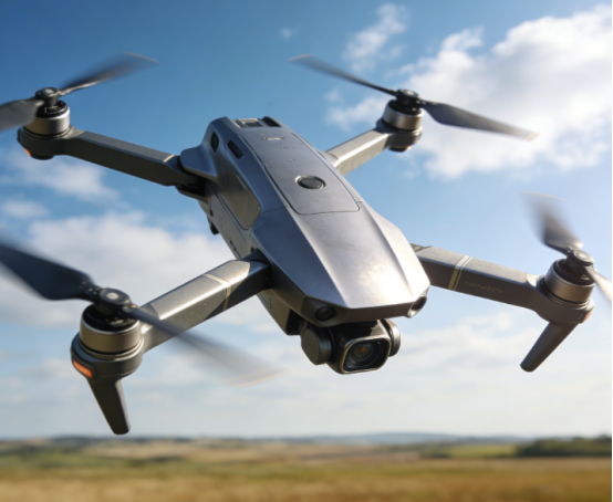
The rapid development of drones has transformed industries ranging from agriculture and logistics to filmmaking and surveillance. At the core of this technological leap is the printed circuit board (PCB), which powers every flight maneuver and sensor reading. As drone technology advances, so too do the demands on PCBs: higher layer counts, denser interconnects (HDI), improved thermal management, more reliable copper thickness control, and stricter dimensional stability.
What Are the Key Functional Requirements for Drone PCBs?
PCBs are the central nervous system of drones, providing both electrical connections and structural support for the electronic components that power the drone. They enable communication between various parts, such as the flight controller, motors, sensors, and battery management system. Essentially, the PCB connects all the vital elements of the drone’s electrical system, ensuring everything works together seamlessly.
To meet the demanding needs of drone technology, PCBs must support high-speed signals, handle high currents, and provide reliable heat management. For instance, the flight controller communicates with sensors on the PCB to adjust the drone’s position during flight. Without the PCB, these components wouldn’t be able to function together efficiently, affecting the drone's stability and maneuverability.
Each module in a drone—whether it’s for controlling flight, managing power, or capturing images—requires a specialized PCB. These boards must not only connect all electrical parts but also withstand physical stress, ensuring that all components are securely held in place. This makes the design and quality of the PCB crucial for the overall performance, reliability, and safety of the drone.
Classification of Drone PCBs
Flight Controller PCB
The flight controller PCB is one of the most critical parts of a drone. It is responsible for processing inputs from various sensors and ensuring the drone’s stability during flight. This PCB needs to handle high-speed signals, control impedance (to prevent signal interference), and maintain excellent EMI (Electromagnetic Interference)/EMC (Electromagnetic Compatibility) performance.
For instance, flight controllers often use HDI (High-Density Interconnect) PCBs to pack a large number of circuits into a small space. This is essential for achieving the high-speed signal transfer required for precise control. To avoid interference from outside sources, flight controller PCBs are also designed to minimize EMI.
Electronic Speed Controller (ESC) PCB
The ESC PCB controls the motors of the drone by regulating the electrical current supplied to them. This PCB must support high current loads and handle significant heat, as ESCs manage the power needed for the motors to spin at various speeds. Therefore, high copper thickness is crucial to carry the large currents, and good heat management techniques are necessary to avoid overheating.
An example of an ESC PCB might use 2–3oz thick copper, which ensures that the high current is efficiently handled while preventing the PCB from overheating.
Power Distribution Board (PDB) PCB
The PDB PCB’s main function is to distribute electrical power from the battery to other components of the drone, such as the flight controller, ESCs, and sensors. Because this PCB handles high current, it also requires thicker copper and robust thermal management. The PDB must also be able to withstand high heat levels without compromising the safety or performance of the drone.
A PDB PCB typically requires copper thickness of 2oz or higher to support reliable power distribution, and it may include additional features such as heat sinks or metalized vias for enhanced cooling.
Battery Management System (BMS) PCB
The BMS PCB is crucial for maintaining the health of the drone’s battery by monitoring its charge, voltage, and temperature. It ensures the safe operation of the battery by preventing overcharging or excessive discharging. The BMS PCB must offer precise electrical stability and accuracy to avoid damaging the battery.
For example, BMS PCBs in larger drones often include sophisticated sensors and control circuits to continuously monitor the battery’s status, ensuring the drone remains operational for longer periods and avoids potential failures during flight.
Communication and Navigation PCBs
These PCBs are responsible for managing high-frequency signals required for communication with the drone’s remote control and GPS navigation systems. The PCB needs to handle high-frequency signals, maintain precise impedance control, and ensure minimal EMI sensitivity to provide reliable communication and accurate positioning.
A typical communication PCB might use small-sized HDI structures to reduce size while maintaining signal integrity, allowing for clear communication and stable GPS tracking.
Imaging and Sensor PCBs
PCBs used for imaging systems (like cameras or visual sensors) in drones need to accommodate high-speed differential signals for data transfer. These PCBs are often lightweight and need to handle the rapid transmission of data while maintaining precise signal integrity. The design must focus on minimizing weight while optimizing performance.
For instance, sensor PCBs for drones may include flexible PCBs or rigid-flex designs that allow the camera or sensor system to fit into compact spaces while keeping the overall weight of the drone low.
Structural Integration PCBs
These PCBs are used to interconnect multiple modules within the drone, such as the flight controller, sensors, and power distribution system. Designed to reduce the need for additional connectors, they improve the drone’s vibration resistance and help maximize space efficiency.
By integrating structural elements directly onto the PCB, drones can save weight, reduce complexity, and improve overall reliability. Flexible PCBs are often used here to ensure durability while maintaining a compact design.
What Are the Key Design Considerations in Drone PCB Manufacturing?
When designing PCBs for drones, several critical factors need to be addressed to ensure optimal performance, reliability, and efficiency. These factors include material selection, signal integrity management, copper thickness optimization for handling high current, and the use of advanced technologies like micro-via and blind hole techniques for miniaturization and higher wiring density.
Material Selection: Ensuring Thermal Stability
The choice of materials is vital to ensure that PCBs maintain excellent performance in the demanding environments that drones operate in. A key consideration is the high glass transition temperature (TG) of the substrate material.
High TG Materials are crucial for thermal stability, especially in components like ESCs and flight controllers, which generate substantial heat during operation. Materials with a TG rating of 150°C or higher prevent the PCB from becoming too soft or deformed under thermal stress. This ensures the PCB can withstand continuous high power usage without warping, preventing circuit failure or signal loss caused by overheating.
Signal Integrity: Managing PCB Layering
Multi-layer PCB designs are commonly used to improve signal integrity and reduce signal interference. By placing power and ground planes on separate layers, designers can shield sensitive signal traces from noise, ensuring that high-speed signals, such as those controlling drone movements, remain unaffected by power signals. This isolation helps minimize signal crosstalk, which is critical for precise control and stability in drone flight. Shielding layers and ground planes also help reduce signal loss and distortion in high-frequency circuits, ensuring clear and accurate signal transmission.
For example, in a flight controller PCB, separating high-speed communication signals from power distribution circuits ensures that the drone’s navigation system remains stable even in environments with fluctuating signals.
Current-Carrying Capacity: Copper Thickness and Via Design Optimization
Copper thickness is a critical factor in ensuring that PCBs can handle the high electrical currents required by drone components like ESCs and PDBs. Thicker copper layers (≥3oz) allow the PCB to carry large currents without overheating or damaging the circuitry. This is particularly important for drones that operate under heavy loads or during long-distance flights. Thicker copper also helps dissipate heat, preventing temperature buildup during prolonged operation.
The via design, which connects different layers of the PCB, also plays a vital role in carrying current. Plated through-holes (PTHs) are typically used for high-current paths to ensure stable conductivity. Optimizing the size and plating of vias ensures that the PCB can handle the required electrical loads without overheating, which is especially crucial for components like ESCs that regulate motor power.
HDI Design: Micro-Via and Blind Hole Technologies
Micro-via technology is key to achieving miniaturization without sacrificing performance in drone PCBs. Micro-vias allow for higher wiring density in compact spaces, enabling more connections in a smaller area. This is particularly beneficial for flight controller PCBs, where space is limited but high-speed signal processing is required. Micro-via technology also helps reduce the distance signals must travel, improving signal quality and reducing the risk of distortion.
In addition, blind and buried vias are used to enhance connectivity and signal integrity in high-density PCB designs. These vias allow internal connections between PCB layers without occupying surface space, essential for maintaining a compact design. However, the reliability of these vias depends on the quality of their plating process. If the plating is subpar, electrical connections may become weak, leading to potential failures.
For example, in a sensor PCB, blind and buried vias can reduce the overall size of the PCB while ensuring reliable connections between internal layers. Properly plated vias are crucial to meet the electrical demands of high-performance sensor systems.
Durability and Reliability: Surface Treatments and Coatings
Surface treatments and coatings are essential to enhance the durability and electrical performance of drone PCBs.
ENIG (Electroless Nickel Immersion Gold) is a widely used surface finish due to its excellent solderability and resistance to oxidation. ENIG provides long-term durability, ensuring stable electrical connections, especially for SMD (surface-mount devices) components. This is particularly important for communication PCBs, which require high-frequency signals to remain clear and uninterrupted, even in harsh environmental conditions.
Lead-Free vs. Leaded Soldering: The choice between leaded and lead-free soldering is critical for the PCB’s long-term stability and environmental compliance. Lead-free soldering is now the standard due to stricter environmental regulations like RoHS. While lead-free solder is environmentally friendly, it may show slightly higher rates of thermal fatigue over time. However, advancements in lead-free solder alloys have minimized these issues, making it reliable for drone PCBs.
Component Mounting: Through-Holes and Surface-Mount Technology
The choice of through-holes versus surface-mount technology (SMT) is another key consideration in PCB design. Through-holes are typically used for larger components, such as power connectors, where durability and stability are needed for high-current paths. In contrast, SMTs are used for smaller components, such as resistors and capacitors, where size and weight are critical factors. SMTs are often used in flight controller PCBs due to their compact size and ability to support high-speed signal processing, reducing the overall weight of the PCB, which is crucial for extending flight times.
For high-current components like those found in ESCs and PDBs, through-holes are necessary to provide secure and durable connections capable of handling heavy electrical loads without failure.
How to Ensure Quality Control in Drone PCB Manufacturing?
Ensuring quality control in drone PCB manufacturing is essential to guarantee that the final product performs reliably in real-world conditions. To achieve this, manufacturers employ a variety of quality control steps to test, inspect, and verify the PCBs at different stages of production.
Key Quality Control Steps in PCB Manufacturing
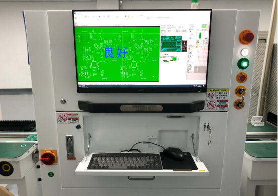
1. Automatic Optical Inspection (AOI): Thorough Inspection of Fine Lines
What is AOI?
Automatic Optical Inspection (AOI) is a non-invasive process that uses cameras and lighting to inspect the PCB for defects, including missing components, misalignment, and poor soldering. AOI is particularly effective at inspecting fine lines and small traces, which are common in HDI PCBs used in drone systems.
Why is it Important?
AOI helps ensure that all the components are correctly placed and that no traces or vias are damaged. For example, in flight controller PCBs, small signal traces need to be perfectly intact to maintain signal integrity. By using AOI, manufacturers can catch errors early, preventing performance issues during flight.
2. X-Ray Inspection: Verifying Connectivity and Plating Integrity of Blind/Buried Vias
What is X-Ray Inspection?
X-ray inspection is a method used to examine the internal layers of a PCB, especially blind holes and buried vias, which cannot be seen by traditional inspection methods. It is used to assess via plating quality and verify the internal connectivity between the PCB’s layers.
Why is it Important?
In drone PCBs, proper via plating is crucial for ensuring stable electrical connections between layers. If these vias are not correctly plated, the PCB may fail under high current, leading to issues such as short circuits. For instance, an improperly connected PDB could result in power loss or instability, affecting drone performance.
Electrical Performance Testing
1. Flying Probe Testing: Verifying Circuit Connectivity and Signal Stability
What is Flying Probe Testing?
Flying probe testing is a method that uses a set of probes to make electrical contact with the PCB to check for continuity, open circuits, and shorts. It is particularly useful for testing the electrical performance of prototype boards or low-volume production.
Why is it Important?
This test ensures that all connections on the PCB are intact and that the electrical pathways are free from defects. For example, in drone PCBs, the signal paths between the flight controller and the sensors must remain stable and free from interruptions. Flying probe testing ensures that the PCB can handle high-speed signals without any disruptions, which is critical for precise control during flight.
2. Impedance Control Testing: Ensuring Stable Signal Transmission
What is Impedance Control Testing?
Impedance control testing ensures that the signal traces on the PCB are designed to maintain the correct impedance. This is crucial for high-frequency signals used in drone communication and sensor systems. The test checks that signal reflections or losses do not occur due to incorrect impedance.
Why is it Important?
In drones, signal integrity is crucial for communication between the flight controller and sensors. If impedance is not correctly controlled, high-frequency signals may suffer from reflections or distortions, leading to inaccurate data transmission or delays. Impedance control testing ensures that the PCB meets the required standards for reliable and stable signal transmission.
Durability Testing and Environmental Simulation
1. Thermal Cycling and Thermal Stress Testing: Verifying Stability Under Temperature Variations
What is Thermal Cycling Testing?
Thermal cycling tests subject the PCB to extreme temperature changes, simulating the environmental conditions that a drone might face during operation. The PCB is heated and cooled repeatedly to test its ability to withstand thermal stress.
Why is it Important?
Drones often operate in environments where the temperature fluctuates significantly, such as during high-speed flights or in varying weather conditions. Thermal cycling ensures that the PCB remains stable and does not suffer from warping or delamination, which could cause electrical failure. For example, a flight controller PCB that is exposed to thermal cycling ensures that high-temperature components, like power transistors, continue to function reliably.
2. Vibration and Shock Testing: Simulating Real-World Flight Conditions
What is Vibration and Shock Testing?
Vibration and shock testing involves subjecting the PCB to mechanical vibrations and shocks to simulate the stresses it would experience in a drone during flight. This helps ensure that the PCB components remain securely in place and that the circuits can withstand the physical stresses of airborne movement.
Why is it Important?
Drones are exposed to vibrations from the motors, propellers, and external factors during flight. These vibrations can cause connections to loosen or components to fail. Vibration and shock testing ensure that the PCB components, such as ESCs and sensors, stay intact and operational, even in challenging flight conditions. Without proper testing, vibrations could lead to unreliable sensor readings or loss of control during flight.
PCBMASTER Drone PCB Case Study Analysis
PCBMASTER has developed a high-performance 6-layer PCB for drone applications, particularly for flight control systems. This case study explores the key features of this PCB design, its manufacturing process, and the rigorous testing methods employed to ensure top performance in demanding environments.
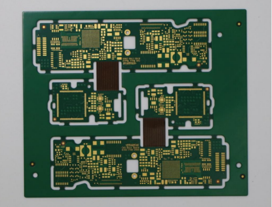
PCB Parameters: 6-Layer Design with Enhanced Copper Thickness
The PCB in question is a 6-layer structure with specific parameters tailored to support high-density wiring and high-speed signal transmission, essential for drone flight control.
Layer Structure: The PCB consists of 6 layers, which enhances signal integrity and allows for complex circuit designs within a compact form factor. Multi-layer designs are critical for separating power, ground, and signal layers to reduce noise and improve the stability of high-speed circuits.
Copper Thickness: The PCB uses 3/3 oz copper thickness for both the inner and outer layers. This thickness ensures the PCB can handle high currents without overheating, which is crucial for components like ESCs and the PDB that demand high power for efficient operation.
Material: The substrate material used is FR-4 with a TG of 150°C, a high-glass transition material that ensures the PCB can withstand extreme temperatures often encountered in drone operations.
Thickness: The overall thickness of the PCB is 1.2mm, optimized for weight savings and compactness without compromising durability or performance.
Surface Treatment: ENIG for Long-Term Stability
The surface treatment used for this PCB is ENIG, which provides significant benefits for soldering and long-term performance.
ENIG Coating: The 0.05μm ENIG process ensures excellent solderability, which is essential for mounting SMDs on the PCB. ENIG also prevents oxidation, ensuring stable electrical connections over time, even under harsh environmental conditions.
Benefits of ENIG: By offering corrosion resistance and a durable gold layer over nickel, ENIG maintains low contact resistance, which is crucial for high-frequency communication and precise control in drones. This finish ensures that the PCB will continue to perform well during extended periods of use.
Manufacturing Process Features: HDI and Micro-Via Technology
PCBMASTER's 6-layer PCB features advanced manufacturing techniques to optimize size and performance. These technologies are essential for creating compact, high-performance boards for drones.
HDI Design: HDI technology is employed to create small vias and traces, enabling dense routing of electrical connections. This helps to minimize the overall size of the PCB without compromising its functionality, allowing for better performance in tight spaces, which is critical for flight controllers in drones.
Micro-Via and Resin Plugged Vias: The use of micro-blind holes and resin-plugged vias further supports high-density routing and ensures stable electrical connections between the PCB layers. Micro-via technology allows for smaller hole sizes, reducing the space taken up by vias and enabling more complex circuitry in a limited space.
Application and Performance
The PCB is designed for flight control systems in drones, where precise control and high-speed signal transmission are vital.
High-Speed Signal Transmission: The 6-layer PCB is engineered to support high-speed signals, which are crucial for drone flight stability. It ensures that data from sensors is transmitted quickly and accurately to the flight control system, allowing for real-time adjustments during flight.
Reliability and Durability: This PCB is built to operate in high-temperature and high-load conditions. The high TG material and thick copper layers ensure the PCB remains stable and durable even in the extreme operational environments that drones are exposed to, such as when flying at high altitudes or carrying heavy payloads.
Quality Control and Testing
Strict quality control and testing procedures are in place to ensure that every PCB meets high-performance standards.
Flying Probe Testing: This testing method checks the electrical performance of each PCB, ensuring that all circuits are correctly connected and free from defects.
Electrical Performance Testing: Detailed testing of the PCB’s electrical characteristics ensures that the board meets the necessary standards for signal integrity, current carrying capacity, and heat dissipation.
X-Ray Inspection: X-ray checks are performed to ensure the integrity of blind holes, buried vias, and internal layers, ensuring that all interconnections are stable and functional.
These rigorous testing methods guarantee that the PCB will perform reliably under real-world conditions, providing the stability and precision required for high-performance drone applications.
Conclusion
Ensuring the quality of drone PCBs is crucial for their performance, reliability, and durability in real-world flight conditions. Through rigorous testing methods like AOI, X-ray inspection, flying probe testing, and impedance control testing, manufacturers can verify the electrical integrity and stability of each PCB. Furthermore, thermal cycling and vibration tests simulate the environmental stresses that drones experience, guaranteeing that the PCBs can handle extreme conditions. By prioritizing these quality control measures, manufacturers can ensure that drone PCBs meet the highest standards, delivering safe and efficient flight experiences.
FAQs
Why does ESC PCB require high copper thickness?
ESC (Electronic Speed Controller) PCBs require high copper thickness to handle the high current loads that the system demands. As drones often operate under heavy loads or high power situations, the electrical components, especially the ESC, need a PCB that can carry substantial current without overheating. Thicker copper layers (≥3 oz) increase the current-carrying capacity of the PCB, ensuring the signals and power are transmitted smoothly, while also improving heat dissipation. This prevents the PCB from overheating, which could lead to component failure or reduced performance in high-load conditions such as heavy lifting or long-distance flights.
How does HDI technology enhance drone PCB design performance?
HDI (High-Density Interconnect) technology significantly enhances drone PCB design by enabling high-density wiring in a compact space. This allows manufacturers to pack more functionality into smaller PCBs without compromising performance. HDI technology uses smaller vias and finer traces, reducing the PCB size while maintaining signal integrity and stability. This is particularly useful in drone applications like flight controllers, where high-speed signal transmission is critical but space is limited. The technology also supports miniaturization, which is essential for meeting the space and weight constraints of drones, ensuring both high performance and compactness.
How is the quality control of drone PCBs performed?
The quality control of drone PCBs is a critical process to ensure their reliability and performance under extreme conditions. Several testing methods are employed, including AOI (Automated Optical Inspection) to check for fine line defects, flying probe testing to validate electrical connections, and electrical performance testing to verify the stability and functionality of the PCB. X-ray inspection is used to assess the quality of blind and buried vias, ensuring proper plating and electrical continuity. These tests help manufacturers detect any potential issues in the PCB before it is used in a drone, guaranteeing high performance and minimal risk of failure during flight.
Why is ENIG surface treatment chosen?
ENIG (Electroless Nickel Immersion Gold) is chosen for PCB surface treatment due to its excellent properties for ensuring stable soldering and long-term reliability. The nickel-gold finish provides excellent resistance to oxidation, which is crucial for maintaining the integrity of the PCB in harsh environments. It also promotes better solderability, making it easier to mount components like surface-mount technologys (SMTs) securely. For drones, which are exposed to vibration, temperature fluctuations, and potential exposure to moisture, ENIG helps ensure stable electrical connections, minimizing the risk of signal degradation or failure over time.
How does PCBMASTER’s PCB case ensure high reliability?
PCBMASTER’s PCB case ensures high reliability through stringent process controls and comprehensive testing methods. The design utilizes HDI and blind/buried via technology, ensuring high-density wiring and compact, efficient layouts. The copper thickness of ≥3 oz ensures the PCB can handle high current demands without overheating, while ENIG surface treatment provides long-lasting protection against oxidation and ensures stable soldering. Rigorous testing like flying probe testing, X-ray inspection, and thermal cycling tests ensures the PCB’s reliability even in extreme environmental conditions. These methods guarantee that the PCB will perform reliably throughout the drone’s lifecycle, even under the most demanding operational conditions.
Author Bio
Hi, I'm Carol, the Overseas Marketing Manager at PCBMASTER, where I focus on expanding international markets and researching PCB and PCBA solutions. Since 2020, I've been deeply involved in helping our company collaborate with global clients, addressing their technical and production needs in the PCB and PCBA sectors. Over these years, I've gained extensive experience and developed a deeper understanding of industry trends, challenges, and technological innovations.
Outside of work, I'm passionate about writing and enjoy sharing industry insights, market developments, and practical tips through my blog. I hope my posts can help you better understand the PCB and PCBA industries and maybe even offer some valuable takeaways. Of course, if you have any thoughts or questions, feel free to leave a comment below—I'd love to hear from you and discuss further!


