


SMD vs. Through-Hole PCB: Which Printed Circuit Board Fits Your Needs?
In the fast-evolving world of electronics, choosing the right printed circuit board can make or break a project. From sleek smartphones to rugged industrial machinery, every device relies on the unseen network of connections beneath its surface. But not all PCBs are created equal—some are designed for precision, miniaturization, and speed, while others excel at durability and mechanical strength. Understanding the differences between these options is key to building electronics that perform reliably and efficiently.
Introduction to PCB Technologies
What is a Printed Circuit Board (PCB)?
A Printed Circuit Board (PCB) is a flat board used to mechanically support and electrically connect electronic components. It forms the backbone of almost all electronic devices, from smartphones and laptops to industrial machines and medical equipment. Components such as resistors, capacitors, and microchips are mounted on the board and connected through copper traces, which act as miniature wires.
The primary function of a PCB is to provide a reliable platform for component interconnection, ensuring that electricity flows correctly through the circuit. Unlike traditional hand-wired circuits, PCBs offer compactness, consistency, and easier assembly, which is essential for modern electronics.
Brief History:
PCBs evolved in the early 20th century, starting as simple single-layer boards with basic conductive paths. By the 1940s, double-sided PCBs allowed circuits on both sides of the board, improving complexity and density. Today, multi-layer PCBs with advanced materials support high-speed signals, miniaturized components, and sophisticated devices like smartphones, servers, and aerospace electronics.
Example: A typical smartphone motherboard is a multi-layer PCB that integrates thousands of SMD components, including processors, memory chips, and sensors, all connected through finely etched copper traces.
Overview of SMD and Through-Hole Technologies
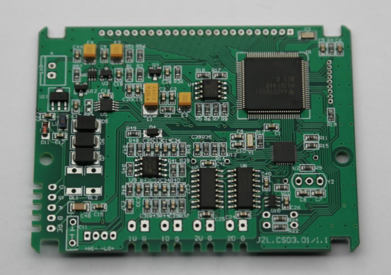
SMD (Surface-Mount Device) PCBs are designed to host components that are soldered directly onto the surface of the board. SMD components are small, lightweight, and ideal for high-density layouts. They are often used in consumer electronics, high-speed communication devices, and wearable technology. Examples include tiny resistors, capacitors, and microcontrollers that fit in millimeter-sized packages.
Through-Hole PCBs, on the other hand, accommodate components with leads that pass through holes in the board and are soldered on the opposite side. This method offers stronger mechanical bonds, making it suitable for components that handle high currents, connectors, and large capacitors. Industrial machinery and automotive electronics frequently use through-hole PCBs for durability and reliability.
High-Level Comparison:
Component Size: SMD components are much smaller than through-hole components.
Assembly: SMD allows automated assembly with pick-and-place machines; through-hole often requires manual or wave soldering.
Board Density: SMD supports higher component density and compact designs.
Mechanical Strength: Through-hole connections provide better physical robustness.
Example Comparison: A compact wearable fitness tracker uses SMD PCBs to save space, while a heavy-duty motor controller in an industrial robot may use through-hole PCBs to ensure secure connections under vibration.
Design Differences Between SMD and Through-Hole PCBs
Component Size and Footprint
SMD components are designed to be extremely small. Common sizes include 0402 (0.04” × 0.02”), 0603 (0.06” × 0.03”), and 0805 (0.08” × 0.05”), which allow for highly compact circuit layouts. These tiny packages make it possible to place hundreds of components on a single board without increasing its overall size.
In contrast, through-hole components are larger and have leads that pass through the PCB. Typical through-hole components include standard resistors, electrolytic capacitors, and DIP (Dual In-line Package) ICs. Their footprint is larger, which limits how many components can fit on a board.
Implications:
Circuit density: SMD PCBs can achieve higher component density, making them ideal for small or portable devices.
Board size: Through-hole PCBs often require larger boards to accommodate bulky components.
Example: A smartwatch motherboard uses 0402 and 0603 SMD components to pack dozens of sensors and chips into a few square centimeters, whereas a power supply PCB for industrial equipment relies on through-hole capacitors and connectors to handle high currents safely.
Layout and Routing Considerations
SMD PCB layouts often use fine-pitch routing, where traces and pads are very close together. Multi-layer boards are common, allowing signals to cross over each other without short circuits. This design enables high-speed signal routing and dense component placement.
Through-Hole PCB layouts require wider traces and more space per component, as leads pass through the board and solder joints are larger. These layouts are generally simpler, but the larger spacing reduces the number of components per board area.
Examples:
A smartphone motherboard uses multi-layer SMD PCBs with thousands of fine-pitch components, routing high-speed data lines on inner layers.
A robotic motor controller uses a through-hole layout with wide traces to handle high currents, ensuring reliability under vibration.
Design Tools and Software
Modern PCB design software supports both SMD and through-hole technologies. Popular tools include:
Altium Designer – supports advanced multi-layer routing and component libraries for both SMD and through-hole.
KiCad – open-source software suitable for designing PCBs with mixed SMD and through-hole components.
Eagle PCB – widely used for hobbyist and small-scale production boards.
Auto-placement and routing features:
SMD: Auto-placement can efficiently position hundreds of tiny components and optimize trace routing for high-density layouts.
Through-Hole: Software assists with lead placement, drill hole alignment, and wave solder preparation, improving accuracy for larger components.
Example Workflow: A designer importing a BOM (Bill of Materials) can use auto-placement to position SMD resistors and capacitors, then manually adjust through-hole connectors for mechanical stability. This hybrid approach speeds up design while maintaining precision.
Manufacturing Processes
Assembly Techniques
SMD Assembly:
Surface-Mount Device (SMD) components are typically assembled using pick-and-place machines and reflow soldering:
1. Solder Paste Application: A stencil applies solder paste onto the PCB pads.
2. Component Placement: Pick-and-place machines precisely position tiny SMD components on the soldered pads.
3. Reflow Soldering: The board passes through a reflow oven, melting the solder and securing the components.
This process is highly automated and suitable for high-density boards and mass production.
Through-Hole Assembly:
Through-hole components are assembled differently, often using wave soldering or manual soldering:
1. Component Insertion: Leads of through-hole components are inserted into PCB holes.
2. Soldering:
Wave Soldering: The board passes over a wave of molten solder, which bonds the leads.
Manual Soldering: For complex or low-volume boards, technicians solder each lead individually.
Through-hole assembly provides strong mechanical connections, making it ideal for components that experience vibration or heavy currents.
Example Workflow Comparison:
A wireless earbuds PCB uses tiny SMD resistors, capacitors, and microcontrollers placed by pick-and-place machines and soldered through reflow, completing assembly rapidly while keeping the board ultra-compact.
A power supply unit PCB for a server rack uses through-hole transformers and large electrolytic capacitors inserted manually or via wave soldering, taking longer but providing strong mechanical support for high-current components.
Production Speed and Scalability
Automation Impact:
SMD assembly benefits from automation, enabling high-volume production with minimal human intervention.
Through-hole assembly is slower due to manual insertion or specialized wave soldering, limiting scalability.
Typical Throughput Comparisons:
A pick-and-place line can place thousands of SMD components per hour.
Manual through-hole assembly may handle only tens to hundreds of components per hour.
Wave soldering improves speed but is still slower than fully automated SMD assembly.
Example: Consumer electronics like smartphones rely on SMD automation to meet millions-of-units production, whereas specialized industrial boards may use through-hole assembly for smaller, durable batches.
Cost Considerations
Equipment and Material Costs:
SMD assembly requires expensive pick-and-place machines, reflow ovens, and stencils.
Through-hole boards require simpler equipment but may need more robust soldering setups.
Labor vs. Automation Costs:
SMD reduces labor costs due to automation, especially for large volumes.
Through-hole relies more on skilled labor, increasing costs for medium or high-volume production.
Batch Production Impact:
Small batches: Through-hole may be more cost-effective due to lower initial equipment investment.
Large batches: SMD is more economical because automation reduces per-unit cost despite higher equipment expenses.
Example: Producing 10,000 smart sensors using SMD technology is cheaper per unit than using through-hole, while producing 50 custom industrial boards might favor through-hole assembly for cost-effectiveness.
Performance Characteristics
Electrical Performance
Signal Integrity and Parasitics:
SMD components generally offer lower parasitic inductance and capacitance because their leads are shorter and closer to the PCB surface. This reduces signal distortion and interference.
Through-hole components have longer leads, which can introduce higher parasitic effects, potentially affecting high-speed signals.
High-Frequency Applications:
SMD PCBs are preferred for high-frequency or high-speed electronics, such as RF modules, 5G devices, and modern processors, because the compact layout minimizes signal loss.
Through-hole PCBs are better suited for low- to medium-frequency applications where signal speed is less critical.
Example Comparison:
A 5G modem PCB uses SMD components to maintain clean high-frequency signal paths.
An industrial sensor interface board using through-hole resistors and connectors handles slower signals but emphasizes durability over speed.
Mechanical Strength and Reliability
Through-Hole Advantages:
Through-hole components provide strong mechanical support, as leads pass through the PCB and solder joints anchor the component firmly.
This makes through-hole PCBs ideal for devices exposed to vibration or mechanical stress.
SMD Reliability:
SMD components are lighter and rely on surface soldering, which can be less robust under extreme thermal cycles or mechanical shock.
However, modern manufacturing techniques, such as reinforced solder paste and underfill materials, improve SMD reliability for most consumer electronics.
Applications Requiring Mechanical Robustness:
Through-hole: Automotive ECU boards, industrial motor drivers, or power supply units.
SMD: Smartphones, tablets, and compact medical devices, where lightweight design and small size are priorities.
Thermal Management
Heat Dissipation:
SMD PCBs can dissipate heat efficiently on small components, but concentrated heat may require thermal vias or copper planes to spread it.
Through-hole PCBs often handle larger currents, and their components may naturally dissipate more heat through leads and bulk material.
Techniques for Thermal Control:
Vias: Transfer heat from surface components to inner or opposite layers.
Copper Planes: Spread heat across the PCB to reduce hotspots.
Heat Sinks: Attached to through-hole components like power transistors or voltage regulators for extra cooling.
Example:
A LED driver PCB uses SMD components with thermal vias and copper planes to prevent overheating in a compact form factor.
A high-power amplifier PCB uses through-hole transistors with attached heat sinks to safely manage large currents and heat.
Applications and Use Cases
Consumer Electronics
SMD PCBs dominate consumer electronics because of their small size, lightweight design, and high component density. Devices like smartphones, laptops, tablets, and wearables require compact boards that can accommodate hundreds of components in limited space.
Example:
A smartphone motherboard uses thousands of SMD resistors, capacitors, and microchips on a multi-layer PCB to handle processing, communication, and power management in just a few square centimeters.
A fitness tracker PCB leverages tiny SMD sensors and microcontrollers to monitor heart rate and motion while keeping the device thin and lightweight.
The SMD approach allows automatic assembly and supports high-speed digital signals, making it ideal for fast-paced consumer electronics markets.
Industrial and Automotive Applications
Through-hole PCBs are widely used in industrial and automotive electronics where mechanical strength and durability are critical. Large connectors, relays, and power-handling components are often mounted using through-hole techniques to ensure reliability under vibration, shock, and extreme temperatures.
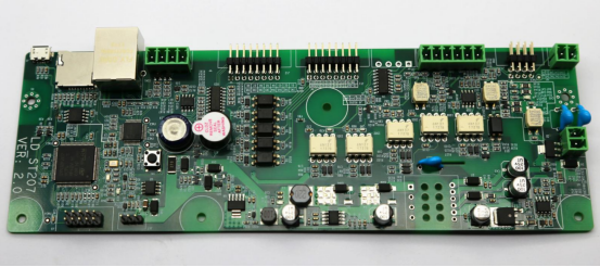
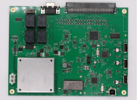
Hybrid PCBs combine SMD and through-hole components on the same board. This approach leverages SMD for space-saving and high-speed circuits, while through-hole components provide strength for heavy-duty or high-current parts.
Example:
An industrial motor controller uses through-hole capacitors and connectors for robustness, while SMD microcontrollers and sensors optimize board size and speed.
A car infotainment system PCB incorporates SMD ICs for processing and through-hole connectors for durable interfaces with external devices.
Medical and Aerospace Electronics
Medical and aerospace devices require exceptional reliability, precision, and long-term stability. The choice of PCB type depends on critical factors like vibration tolerance, heat management, and miniaturization.
SMD PCBs are preferred for compact medical devices such as portable monitors or wearable diagnostics, where board size and signal performance are priorities.
Through-hole PCBs are often used in aerospace avionics, large medical imaging equipment, and implantable devices where mechanical robustness and secure connections are essential.
Example:
A pacemaker PCB may use through-hole components for battery and connector interfaces, while incorporating SMD ICs for signal processing to minimize size.
Satellite control boards combine SMD components for high-speed data handling with through-hole connectors to withstand launch vibration and thermal extremes.
Choosing the Right PCB for Your Project
Factors to Consider
When selecting between SMD and through-hole PCBs, several key factors should guide the decision:
Budget, Production Volume, and Time-to-Market:
SMD PCBs often require higher initial investment in automated assembly equipment but reduce per-unit cost for large-scale production.
Through-hole PCBs may be more cost-effective for small batches or prototypes, but assembly is slower.
Time-to-market can be faster with SMD due to automation and efficient component placement.
Component Availability and Sourcing:
SMD components are widely available for consumer electronics, high-speed circuits, and modern devices.
Through-hole components are preferred when sourcing high-power or heavy-duty components, connectors, and mechanical interfaces.
Required Board Size, Weight, and Density:
SMD allows compact, lightweight boards with high component density.
Through-hole requires larger footprints but provides mechanical stability for heavy or vibration-prone components.
Example: A startup designing a small wearable device may choose SMD to save space and speed up assembly, while a manufacturer building a heavy-duty industrial power supply may use through-hole to ensure durability.
Decision-Making Framework
A step-by-step approach helps determine the right PCB type:
Define Project Goals: Consider size, weight, speed, and durability requirements.
Assess Production Volume: Determine if the project will be mass-produced or limited-run.
Evaluate Component Needs: Identify whether components are SMD-only, through-hole, or both.
Consider Budget and Time Constraints: Compare the cost of automated SMD assembly versus manual through-hole processes.
Choose PCB Type:
SMD: Best for small, lightweight, high-speed boards with dense layouts.
Through-Hole: Best for robust, high-current, or vibration-sensitive applications.
Hybrid PCB: Use SMD and through-hole together when both speed/compactness and mechanical strength are needed.
Example Scenario Comparisons:
Scenario 1: A drone flight controller requires lightweight and compact PCB for high-speed signal processing → choose SMD.
Scenario 2: A factory motor controller handles high currents and vibration → choose through-hole.
Scenario 3: A hybrid IoT gateway requires dense digital circuitry and strong connectors → choose hybrid SMD + through-hole PCB.
Conclusion
SMD and through-hole PCBs each bring unique strengths to electronics design. SMD boards excel in compactness, high-density layouts, and high-speed signal performance, making them ideal for consumer electronics, wearables, and compact medical devices. Through-hole PCBs offer mechanical robustness, reliability under vibration, and high-current handling, which suits industrial equipment, automotive systems, and aerospace applications. In many cases, hybrid PCBs combine the advantages of both technologies, enabling dense circuitry alongside durable connectors or power components.
Looking ahead, PCB technology is evolving rapidly. Hybrid boards and advanced packaging techniques allow designers to balance performance, size, and durability like never before. Emerging materials and miniaturization trends continue to push the boundaries of speed, heat management, and device integration. For designers, engineers, and manufacturers seeking guidance or tailored solutions, PCBMASTER offers professional expertise and support to help select the right PCB type, optimize layouts, and meet project-specific requirements.
FAQs
Can SMD components be used on Through-Hole PCBs?
Yes, SMD components can sometimes be used on through-hole PCBs, but there are limitations. Through-hole boards are designed with holes for leads, so SMD components may need adapters or modification to mount on the surface. In practice, most SMD components are intended for surface-mount pads, so direct use on a traditional through-hole PCB is uncommon. Hybrid PCBs that combine through-hole and SMD pads are a better solution when both types of components are needed.
Which PCB type is better for prototyping vs. mass production?
Prototyping: Through-hole PCBs are often preferred because they allow manual assembly and easier component replacement, making testing and iteration simpler.
Mass production: SMD PCBs are ideal due to automation with pick-and-place machines and reflow soldering, enabling faster assembly, higher density, and lower per-unit costs in large volumes.
How does PCB thickness affect SMD vs. Through-Hole performance?
PCB thickness influences mechanical strength, heat dissipation, and signal integrity:
SMD PCBs: Thinner boards are common to save weight and reduce signal path length, but extremely thin boards may require careful thermal management using copper planes and vias.
Through-hole PCBs: Thicker boards are often needed to support large components and heavy currents, providing mechanical stability and better solder joint strength under vibration or thermal stress.
Are there hybrid PCBs that combine both technologies?
Yes, hybrid PCBs integrate both SMD and through-hole components on the same board. This approach leverages the compact, high-speed advantages of SMD for digital or signal processing circuits while maintaining the mechanical strength of through-hole components for connectors, large capacitors, or power-handling parts. Hybrid boards are common in industrial control systems, automotive electronics, and complex IoT devices.
How does environmental stress impact SMD and Through-Hole reliability?
SMD components: Lighter and smaller, SMD components can be more sensitive to thermal cycling, vibration, and mechanical shock, but modern manufacturing techniques, such as reinforced solder paste and underfill, enhance their reliability.
Through-hole components: With leads passing through the PCB, through-hole components are more resilient under vibration and mechanical stress, making them suitable for industrial, automotive, and aerospace applications where durability is critical.

