


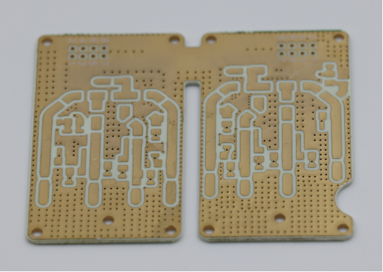
7 Essential PCB Layout Tips for Better Performance and Efficiency
The layout of components on a PCB is crucial. A well-organized layout not only makes the board visually neat and tidy but also affects the length and number of the traces. A good PCB component layout is essential for enhancing the overall performance of the device.
So, how can you make the layout more efficient? In this article, we'll explore essential PCB layout tips for better performance and efficiency.
Tip 1: How to Optimize Wireless Module Placement on PCB Layout?
To optimize wireless module placement on a PCB layout, it's crucial to minimize interference and ensure reliable signal transmission. This involves strategically separating analog and digital circuits, avoiding noise from sensitive components, and carefully positioning the antenna. By following these guidelines, you can significantly enhance the wireless module's performance and ensure smooth communication within your device.
Separation of Analog and Digital Circuits
To optimize the placement of a wireless module, it’s important to physically separate the analog and digital circuits. For example, the MCU (Microcontroller Unit) and the wireless module’s antenna should be placed at a sufficient distance from each other. This is because analog circuits are sensitive to noise from digital circuits, and placing them too close can cause signal interference. By keeping them apart, you reduce the risk of cross-talk and signal degradation.
Real-life example: If the MCU and the wireless module antenna are too close, the MCU’s high-speed digital signals can interfere with the radio frequency (RF) signals from the antenna, reducing the range and performance of the wireless communication.
Avoiding Sensitive Components Under the Wireless Module
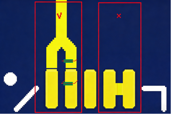
It’s essential to avoid placing high-frequency digital and analog traces beneath the wireless module. Components such as high-speed signal traces, power lines, or sensitive analog circuitry should not be directly below the wireless module. These components can introduce noise or unwanted interference that could affect the wireless signal quality.
A good practice is to pour copper under the wireless module. This provides a stable ground and shields the module from electrical noise coming from the board below. Additionally, the copper pour helps reduce electromagnetic interference (EMI) and improves the overall signal integrity of the wireless module.
Placement Near Power Components
When placing the wireless module on the PCB, it’s important to keep it away from power components like transformers, power inductors, and high-current power traces. These components generate electromagnetic interference (EMI), which can negatively affect the performance of the wireless module.
To further improve performance, consider adding shielding around the wireless module. Shielding can prevent external EMI from entering the module and prevent the module's signals from interfering with nearby components. A proper shielded enclosure around the wireless module can be used to isolate the antenna and circuit from power and noise-sensitive parts.
Antenna Placement and PCB Design
Proper antenna placement is key to achieving optimal wireless performance. The antenna, whether it’s an onboard PCB antenna or ceramic antenna, should have a clear ground plane directly beneath it. This helps create a stable environment for RF signals and enhances the antenna’s radiation pattern.
It’s crucial to avoid copper pours directly beneath the antenna, as this can block the RF signal and reduce antenna efficiency. The antenna should also be placed near the edge of the PCB. This positioning ensures better radiation efficiency and allows the signal to be transmitted more effectively without being obstructed by surrounding components. Placing the antenna at the edge maximizes its line-of-sight to the surrounding environment, improving its communication range and signal strength.
Tip 2: What Are the Best Practices for Trace Width and Spacing in PCB Design?
To ensure optimal performance and reliability in PCB design, it's essential to carefully calculate trace width and trace spacing. These factors determine how well the PCB handles power and signal transmission, minimizing issues like heat buildup, interference, and signal degradation. By following best practices for trace width and spacing, you can improve the overall efficiency and longevity of your design.
Trace Width Calculation for Power and Signal Traces
When designing a PCB, calculating the proper trace width is essential for both power and signal traces. The width determines how much current a trace can safely carry without overheating or causing voltage drops.
Key considerations for calculating trace width include:
Current Load: The amount of current the trace will carry directly affects the required width. Higher current requires wider traces.
PCB Copper Thickness: The thicker the copper, the more current the trace can carry without excessive heating. Common copper thicknesses are 1oz or 2oz per square foot.
Trace Length: Longer traces result in greater resistance, so the width may need to be adjusted accordingly.
For example, to safely carry 2A of current with 1oz copper (which has a thickness of around 0.035mm), the trace width should be approximately 1.0mm. This ensures the trace can handle the current without excessive heating or power loss.
Signal Integrity and Trace Spacing
Maintaining proper trace spacing is critical to ensure the signal integrity of a PCB. Traces that are too close can interfere with each other, causing crosstalk or unwanted noise. This is especially important for high-speed signals, where any disruption in the signal can affect performance.
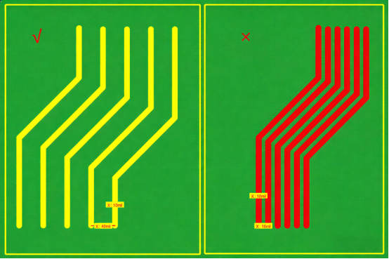
A common guideline to prevent interference is the "3W Principle", which recommends that the center-to-center spacing between traces should be at least three times the trace width. This creates enough space to ensure that signals do not interfere with one another, maintaining clean and reliable data transmission.
Example: If a trace width is 0.5mm, the spacing between traces should be at least 1.5mm to reduce crosstalk and ensure signal integrity.
Power Trace Layout
Designing power traces requires extra attention, as these traces carry higher currents and must be designed for reliable current flow. The trace width for power lines should be calculated based on the current load and desired voltage drop.
For high-current power traces, a good strategy is to make them wider to reduce resistance and heat buildup. This is especially important for circuits that supply power to devices such as microcontrollers or wireless modules, which can draw significant current.
Additionally, for RF traces, the trace width needs to be optimized for impedance matching. The 50Ω characteristic impedance is common for RF traces. For example, a trace width of 0.55mm might be ideal for RF signals with power up to 30dBm. The exact width depends on the specific frequency and the PCB stackup.
Practical Tips for Spacing Between Different Types of Traces
Different types of traces, such as signal traces, power lines, and high-speed signals, each require specific spacing to ensure optimal performance.
Signal Traces: For standard signal traces, ensure a 3W spacing to avoid interference. For high-speed signals, additional shielding or separation may be necessary to maintain signal quality.
Power Lines: Power traces should be kept wider to handle higher current. Power traces can be placed closer together than signal traces but should be spaced far enough to prevent excessive heat buildup and interference with nearby components.
High-Speed Signals: For high-speed or differential signals (like USB or Ethernet), spacing should be tight to minimize trace length but still maintain proper impedance and minimize noise.
By considering these differences, you can ensure that the traces on your PCB will carry signals and power efficiently without unwanted interference or degradation in performance.
Tip 3: How to Manage Component Spacing in PCB Layout?
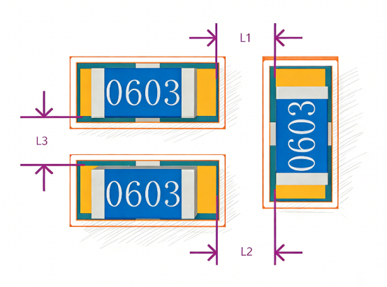
Proper component spacing in PCB layout is essential for smooth manufacturing, reliable soldering, and overall device performance. To achieve a successful design, it's important to consider factors like component height, package type, and the needs of the assembly process. By following best practices for spacing, you can ensure that components are easy to assemble, avoid manufacturing defects, and optimize your PCB for reliability and efficiency.
Minimum Spacing for Soldering and Manufacturing
Managing the spacing between components is crucial for both soldering and manufacturing processes. Adequate spacing ensures smooth assembly, easy soldering, and reliable connections.
For similar components (e.g., resistors or capacitors), a minimum spacing of 0.3mm is typically recommended. This allows for enough room for the soldering process and helps prevent issues like solder bridges or component damage. For hand-solderable parts, the spacing should be increased to 1.5mm or more to allow for easier manual soldering.
Inadequate spacing can lead to production issues such as difficulty in soldering, poor yield rates, and increased chances of short circuits. Too little space can make it hard for automated machines to handle the parts correctly, increasing the chance of defects. Therefore, proper spacing is essential for improving the overall manufacturing efficiency and ensuring a higher-quality product.
Handling High and Low-profile Components
When designing a PCB, it's important to consider the height differences between components, particularly high-profile and low-profile components. These components can interfere with each other if not spaced properly.
For high-profile components (e.g., large capacitors or heatsinks), allow extra space above and below them to avoid physical interference with nearby components. Similarly, low-profile components (e.g., small resistors) need less vertical space but must still be placed with care to avoid crowding.
For components with large height differences, extra attention is needed to ensure proper mechanical clearance. If high-profile components are too close to low-profile ones, they might cause physical stress on the PCB during assembly or use, leading to damage or malfunctions. A good practice is to ensure that component height variations are accounted for in both vertical and horizontal spacing to allow proper airflow and assembly.
Interfacing Different Package Types
When mixing different package types on a PCB, such as through-hole and SMD (Surface-Mount Devices), proper spacing is vital to ensure that both types are correctly assembled and soldered.
Through-hole components require more space around their leads for effective soldering, especially when placed near SMD components, which are typically placed flat against the PCB. The spacing between through-hole and SMD parts should be sufficient to prevent solder bridging and allow for automated assembly processes.
A common guideline is to maintain 1-3mm of spacing between through-hole leads and SMD pads to allow enough room for pick-and-place machines and wave soldering processes. If the spacing is too tight, it can lead to assembly difficulties, higher risk of soldering defects, and reduced production yield.
Tip 4: How to Control Board Edge and Trace Distance for Reliability?
Controlling the distance between components, traces, and the edge of the PCB is crucial for ensuring the board's reliability and manufacturability. Proper spacing helps prevent damage during panel separation, handling, and assembly. In this section, we'll explore best practices for managing board edge and trace placement to enhance the durability and performance of your PCB design.
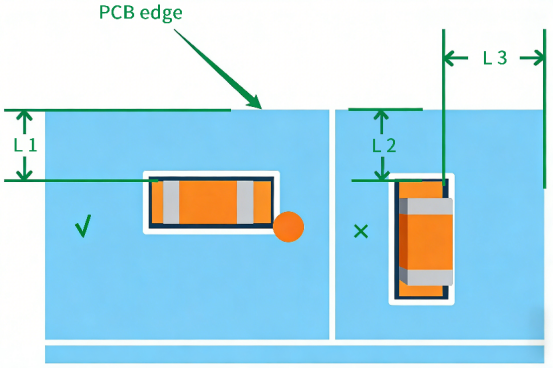
Risks of Inadequate Distance to PCB Edge
Placing components or traces too close to the PCB edge can cause significant issues during manufacturing and affect the long-term reliability of the board. When components or traces are too near the edge, they are at risk of damage during processes like panel separation. During panelization, the PCB is often separated into individual boards, and if components are too close to the edge, they may get damaged or even cause pad detachment. This can result in costly manufacturing defects and reduced product quality.
To minimize these risks, it’s recommended to keep a minimum distance of 0.5mm between components and the PCB edge. This ensures that components are protected during handling and that there’s enough space for manufacturing processes like panelization and assembly.
For example, if a component is placed too close to the edge, it could get caught during the routing process, leading to pad detachment, which makes the board unusable or more expensive to repair. By keeping components within the recommended distance from the edge, you help avoid these common manufacturing issues.
Optimal Trace Placement Near Board Edges
When placing traces near the PCB edge, special care should be taken to ensure signal integrity and reliability. Traces that run too close to the edge are at risk of breaking or disconnecting during handling or assembly, particularly during PCB panel separation or subsequent mechanical stress. This is especially critical for high-speed signals or sensitive traces that require precise routing.
To ensure optimal placement, traces should be positioned at least 0.5mm from the edge to avoid these risks. Additionally, it’s important to ensure that no critical traces are routed along the edges where they can be easily damaged. Keeping traces well within the board’s perimeter helps to prevent mechanical failure, reduces stress on components, and improves the overall durability of the PCB during assembly and operation.
Tip 5: What Is the Importance of Proper Pad and Via Design in PCB Layout?
Proper pad and via design is critical for ensuring the reliability and performance of a PCB. The way vias and pads are placed, sized, and connected directly impacts signal integrity, current-carrying capacity, and the ease of soldering during assembly.
Via Placement and Sizing for Signal Integrity
The placement and sizing of vias in PCB design are crucial for both signal integrity and current-carrying capacity. Vias are used to connect different layers of the PCB, and if they are too small or poorly placed, they can disrupt signals, leading to issues like signal degradation, cross-talk, or even failure of the circuit to work correctly.
Choosing the right via size depends on the amount of current the via needs to carry and the type of signal it will carry. For example, a via carrying high current may need to be larger in diameter to avoid overheating or excessive resistance.
Improper via placement can also affect the performance of critical components. For instance, placing vias too close to high-speed signal traces or sensitive components can cause interference or unwanted coupling. This is especially important in high-frequency circuits where even small changes in impedance can cause signal reflection or loss.
Via-to-Pad Connection
One of the most important considerations in via design is ensuring a proper via-to-pad connection. It’s essential not to place a via directly under a pad because it can cause significant soldering issues. When a via is placed directly under a pad, it makes the soldering process more difficult and can result in poor solder joints or cold soldering, which can lead to unreliable connections.
A recommended practice is to position vias away from pads or connect them using a solder mask bridge or pad-to-via connection. This ensures a smooth and reliable soldering process, improving both the quality and durability of the solder joints.
Tear Drops and Fillet Additions for Reliability
Adding tear drops and fillet shapes around vias helps improve the mechanical strength and signal integrity of a PCB. A tear drop is a smooth, rounded shape that connects a via to a trace or pad, reducing the sharp angles that can cause stress on the PCB material. This reduces the chance of trace breakage or via failure, especially during thermal cycling or mechanical stress in the field.
In addition to improving the mechanical strength, tear drops can help prevent signal reflections at via connections by providing a smoother path for signals. This is particularly important for high-speed signals, where sharp edges can cause impedance mismatches and signal degradation. By using tear drops and fillets, you ensure that the board can handle higher frequencies and stress without performance issues.
Tip 6: How to Optimize Through-Hole Design in PCB Layout?
Optimizing through-hole design in PCB layout is crucial for ensuring both performance and cost-efficiency. Proper via size, placement, and type are essential for minimizing signal interference, maintaining signal integrity, and managing manufacturing costs.
Choosing the Right Via Size and Type
Selecting the appropriate via size and type is a crucial step in PCB layout design. Through-hole vias are used to connect different layers of the PCB, and their size and type can significantly affect signal integrity, power distribution, and overall circuit performance.
1. Signal vs. Power Vias:
Signal vias carry low to moderate-frequency signals. These vias typically have smaller diameters and are used in less demanding applications.
Power vias, on the other hand, carry higher currents and are typically larger in diameter to handle the increased current without overheating. Choosing the right via size helps ensure that the board can handle both signal and power requirements efficiently.
2. Impact of Via Diameter and Length:
The via diameter and length affect the overall impedance, resistance, and inductance of the circuit. Larger vias have lower resistance and can carry more current, but they also take up more space and cost more to manufacture.
For high-frequency designs, it’s essential to minimize the via length and choose a smaller diameter to reduce inductance and prevent signal degradation. Long vias or large vias can introduce unwanted inductive reactance that interferes with high-speed signals, leading to performance issues like signal reflections or loss.
Via Placement for Minimizing Electromagnetic Interference
Proper via placement is key to minimizing electromagnetic interference (EMI) and maintaining signal integrity. Incorrect via placement can result in signal coupling, where signals from different layers interact in unwanted ways, causing noise or distortion.
Best practices include:
1. Avoid Placing Vias Near Sensitive Traces: Vias should not be placed directly under high-speed signal traces or near critical components to avoid coupling and EMI.
2. Distance from Power and Ground Vias: Power vias should be placed carefully to avoid coupling with signal vias. Grouping power and ground vias separately from signal vias reduces the likelihood of interference and helps maintain clean signals.
3. Minimize Via-to-Via Proximity: Vias placed too close to one another can cause crosstalk, where signals from one via bleed into adjacent vias. Keeping adequate space between vias ensures better isolation and reduces noise.
Cost and Performance Tradeoffs
When designing through-hole vias, balancing cost with performance is essential. While larger or more numerous vias may improve circuit performance, they also increase manufacturing costs and PCB complexity.
1. Balancing Via Size, Number, and Placement:
Larger vias can handle more current and reduce signal loss, but they take up more space and increase the cost of drilling.
The number of vias should be minimized to reduce the complexity of the PCB and lower costs. However, reducing the number of vias too much can lead to performance issues like excessive trace length, which can increase resistance or introduce noise.
2. Minimizing Via Count:
Reducing the total via count can also help reduce the overall complexity of the board, making it easier to manufacture and test. This is especially important in high-volume production where minimizing cost is critical.
Blind vias or buried vias can also be used strategically to reduce the number of visible vias on the PCB, though these come at a higher manufacturing cost.
Tip 7: How to Improve Power Integrity in PCB Layout?
Improving power integrity in PCB layout is essential for ensuring stable and reliable operation of electronic circuits. Proper power trace design, strategic placement of decoupling capacitors, and solid grounding all play a crucial role in minimizing noise and voltage ripple.
Power Trace Design for Low Voltage Ripple
Ensuring low voltage ripple is essential for stable power delivery, especially in wireless modules and other sensitive electronic devices. Voltage ripple refers to unwanted fluctuations in voltage that can lead to noise, poor performance, or even malfunction in circuits that rely on stable power.
1. Selecting Appropriate Trace Widths:
The trace width for power distribution must be chosen based on the current load and the acceptable voltage ripple. Wider traces have lower resistance, which helps reduce the ripple in the power supply. For low voltage ripple, you should select wider power traces to handle the current load without causing excess heat or voltage drops. Typically, for higher current applications, a larger trace width will minimize voltage fluctuations and ensure stable power.
2. Placement of Decoupling Capacitors:
Decoupling capacitors are key components for reducing noise and stabilizing the power supply. They should be placed as close as possible to the power pins of sensitive components, such as MCUs or wireless modules. This helps filter out high-frequency noise and smoothens the power delivered to the device. The capacitors act as local energy reservoirs, providing quick bursts of power when needed, and reducing the impact of ripple.
For example, in a wireless module, placing decoupling capacitors near the power input helps prevent interference from voltage spikes or power fluctuations, ensuring the module operates reliably.
Ensuring Solid Grounding for Power and Signal Integrity
A solid grounding system is critical for maintaining both power integrity and signal integrity in PCB design. Poor grounding can cause ground loops, which lead to noise, signal interference, and erratic behavior in electronic circuits.
1. Importance of Solid Grounding:
A solid ground plane ensures that power and signal returns have low impedance paths to follow. This helps maintain stable voltage levels and reduces the chances of unwanted electromagnetic interference (EMI). Without proper grounding, the return currents for power and signals can create noise that interferes with the performance of sensitive components, especially in high-speed or high-frequency circuits.
For instance, without a solid ground plane, a high-speed signal trace might pick up noise from the power plane, causing data corruption or signal degradation.
2. Use of Ground Pours and Ground Vias:
Ground pours are large copper areas used to create a continuous and low-impedance path for the ground return. These pours should cover as much of the PCB as possible, especially around power traces and sensitive components. In addition, ground vias connect the ground pours across multiple layers of the PCB, ensuring that the entire board shares a common, low-impedance ground.
By using ground pours and vias, you ensure that the ground path remains as short and direct as possible, reducing the risk of voltage fluctuations or signal noise caused by poor grounding.
Conclusion
Optimizing your PCB layout is critical to ensuring the reliability, performance, and manufacturability of your electronic devices. From component placement and trace width selection to grounding and power integrity, every decision impacts your PCB’s functionality. As a seasoned PCB supplier, PCBMASTER has the expertise to help you design the most efficient and reliable PCB layouts. Whether you're tackling complex designs or optimizing for performance, our team is ready to assist you in creating high-quality, high-performance PCBs tailored to your needs. Let us partner with you to bring your projects to life with precision and reliability.
FAQs
Why is Component Spacing Crucial in PCB Design?
Correct component spacing is essential in PCB design for several reasons:
1. Avoiding Manufacturing Issues: If components are placed too close together, it can lead to problems during assembly, such as solder bridges or short circuits. It also complicates automated soldering or manual soldering processes, which increases the risk of defects like poor solder joints or damage to components. For example, placing a high-density set of components too close may cause the pick-and-place machine to misplace parts, leading to manufacturing delays and increased costs.
2. Signal Integrity Problems: When components are too close, traces can interfere with each other, causing crosstalk or signal degradation, especially in high-speed circuits. Proper spacing helps maintain clear paths for signal transmission, reducing the risk of noise and signal interference.
3. Ease of Soldering: Adequate spacing ensures that soldering can be done efficiently and accurately, minimizing the chance of cold solder joints, which can lead to intermittent connections or failure in the circuit. This is especially critical in hand-soldering and high-precision assembly.
In short, proper component spacing is key to maintaining manufacturing efficiency, signal quality, and assembly reliability in PCB designs.
What is the "3W Principle" in PCB Design?
The 3W Principle in PCB design refers to maintaining a safe distance between traces based on their width. Specifically, the 3W rule states that the center-to-center distance between traces should be at least three times the width of the trace. This principle is crucial for:
1. Maintaining Proper Isolation: Ensuring that traces are far enough apart prevents signal interference (such as crosstalk) and ensures that each trace can operate without causing unwanted inductive or capacitive coupling. This is especially critical for high-speed signals or analog circuits.
2. Preventing Short Circuits and Signal Degradation: The rule helps to prevent accidental shorts due to manufacturing tolerances and ensures that signal integrity is preserved over long distances or through different PCB layers. For instance, if two power traces are too close together, they may cause overheating or unwanted current leakage, leading to poor circuit performance.
3. Ensuring Safe Signal Transmission: For high-frequency designs, the 3W rule ensures that signal lines, power lines, and ground traces are appropriately spaced to minimize electromagnetic interference (EMI) and ensure that signals can propagate without degradation.
Importance: By following this principle, you can ensure that your PCB layout supports both signal fidelity and electromagnetic compatibility (EMC), which is vital in high-speed and sensitive applications like wireless communication or analog signal processing.
How Can I Minimize EMI in My PCB Layout?
Minimizing electromagnetic interference (EMI) is critical to maintaining the performance and reliability of your PCB, especially in high-speed circuits. Here are some practical steps to reduce EMI in your layout:
1. Component Placement:
Separate sensitive components (e.g., analog or RF circuits) from high-speed digital components to prevent noise coupling. Keep components like oscillators, voltage regulators, and high-current traces away from sensitive signal paths.
Position decoupling capacitors close to power pins to minimize noise and smooth voltage fluctuations.
2. Use Ground Planes:
A solid ground plane beneath high-speed traces helps reduce EMI by providing a low-impedance path for return currents. It also helps shield sensitive components from external noise.
Use ground pours to cover as much of the PCB area as possible, ensuring there are minimal gaps in the ground connection.
3. Trace Routing:
Keep signal traces short and direct to minimize their exposure to external interference.
For high-speed signal traces, ensure they are shielded by ground planes or use differential pairs that help cancel out electromagnetic interference.
4. Use Proper Trace Widths:
For power traces, use wider traces to lower resistance and minimize voltage ripple. This prevents the power supply from generating noise that can affect nearby sensitive traces.
5. Use EMI Shielding:
Shielding can be used to contain and direct EMI away from critical areas of the PCB. Shielding enclosures or copper traces around sensitive components can help keep noise in check.
By implementing these techniques, you can significantly reduce EMI, improving the signal integrity and overall performance of your PCB, especially in wireless, high-frequency, and high-speed applications.
What Role Do Vias Play in High-Frequency PCB Design?
Vias play a critical role in multi-layer PCBs, especially in high-frequency designs, where signal integrity and impedance control are essential. Here’s how vias impact your design:
1. Via Type, Size, and Placement:
Via Size: The size of the via impacts the impedance and resistance of the circuit. Larger vias have more resistance and inductance, which can affect signal integrity. Small vias reduce these issues but may not carry enough current for high-power designs.
Via Type: In high-speed designs, using blind or buried vias can help reduce the overall via length, minimizing signal loss and reflection. Microvias are also a good option for high-density designs, especially in RF circuits, as they have lower inductance compared to traditional vias.
Via Placement: Vias should be placed away from high-speed traces to avoid signal interference. They should also be avoided under components where the via could interfere with soldering or introduce inductance that can degrade high-speed signals.
2. Via Impact on High-Speed Signal Integrity:
Via Inductance: Vias introduce inductance into high-frequency signals, which can cause signal reflection or degradation if not carefully managed. The longer the via, the greater the inductance. By keeping vias as short and direct as possible, you can reduce their negative impact on signal quality.
Via-to-Via Coupling: Vias placed too close to each other can cause crosstalk, where signals from one via interfere with signals from another. Proper via placement and spacing are essential to ensure low noise and signal integrity.
In high-frequency PCB design, via optimization is crucial to prevent unwanted effects such as signal distortion or interference. Minimizing via length and choosing the right size and type for your application can ensure clean signal transmission and preserve overall circuit performance.
How Should I Handle Power Supply Layout in High-Speed PCBs?
Designing an effective power supply layout for high-speed PCBs is essential to maintain noise-free performance and ensure reliable operation. Here are some key tips for managing power supply layout:
1. Power Trace Design:
Use wide power traces to minimize resistance and prevent voltage drops that could affect performance, especially when high currents are involved.
Route power traces as directly as possible, minimizing unnecessary bends or detours that can introduce additional impedance and noise.
2. Decoupling Capacitors:
Decoupling capacitors should be placed close to power pins of critical components to reduce high-frequency noise and smooth out any voltage ripple.
Use capacitors of different values (e.g., 10μF, 0.1μF) to cover a wide range of frequencies and ensure effective filtering across the PCB.
3. Separate Power and Ground Planes:
Use separate power and ground planes for clean separation of high-speed signals and noisy power traces. This prevents power fluctuations from affecting signal integrity.
Ensure that the ground plane is continuous and low-impedance to minimize noise coupling.
4. Use of Power Gating:
For circuits that require variable power, use power gating to selectively provide power to different parts of the PCB. This minimizes the risk of unwanted noise coupling into sensitive parts of the circuit.
By carefully designing the power supply layout and integrating decoupling capacitors, grounding techniques, and wide traces, you can ensure that the PCB operates efficiently and without noise, even in demanding high-speed applications.
Author Bio
Hi, I'm Carol, the Overseas Marketing Manager at PCBMASTER, where I focus on expanding international markets and researching PCB and PCBA solutions. Since 2020, I've been deeply involved in helping our company collaborate with global clients, addressing their technical and production needs in the PCB and PCBA sectors. Over these years, I've gained extensive experience and developed a deeper understanding of industry trends, challenges, and technological innovations.
Outside of work, I'm passionate about writing and enjoy sharing industry insights, market developments, and practical tips through my blog. I hope my posts can help you better understand the PCB and PCBA industries and maybe even offer some valuable takeaways. Of course, if you have any thoughts or questions, feel free to leave a comment below—I'd love to hear from you and discuss further!


