


QFP (Quad Flat Package) Guide: Design, Assembly, and Key Pros & Cons
The way a chip is packaged plays a crucial role in its performance and how easily it integrates into devices. The Quad Flat Package (QFP) is one such design that balances functionality, ease of manufacturing, and cost-effectiveness. With its signature gull-wing leads and flat profile, QFP has become a staple in everything from consumer electronics to automotive systems. As we dive into its details, you'll see why this package continues to be a top choice for engineers and designers around the world.
Introduction to QFP (Quad Flat Package)
What is QFP?
Definition of Quad Flat Package (QFP)
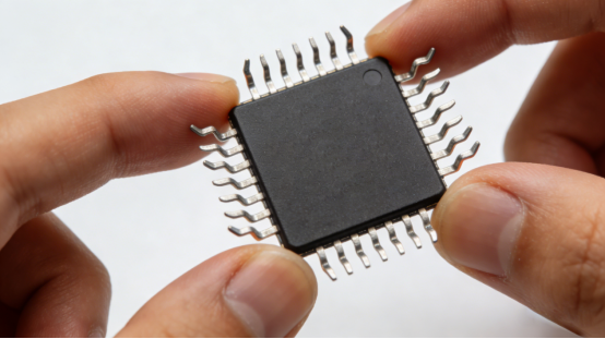
The Quad Flat Package, commonly referred to as QFP, is a type of surface-mount package used to house semiconductor chips. It features a flat, rectangular or square body with leads (metallic contacts) that extend outward in a "gull-wing" shape from all four sides of the chip. These leads make it easy to connect the chip to a circuit board.
Explanation of Key Features
Flat Design: The QFP has a low-profile, flat body, making it ideal for compact electronic devices like TVs, printers, and smartphones. The flat design allows the package to fit in tight spaces without adding extra bulk.
Gull-Wing Leads: The leads on a QFP are bent outward in a gull-wing shape, making them highly visible and easy to inspect. This design helps in soldering the leads to the circuit board with accuracy, reducing the chance of mistakes during assembly.
Surface-Mount Technology (SMT): QFP packages are made for surface-mount technology, which means they are designed to be placed directly onto the surface of a circuit board. This is different from through-hole technology, where leads pass through the board.
Importance in Electronic Packaging
QFP plays a crucial role in electronic packaging because it strikes a balance between size, cost, and ease of assembly. It can accommodate a moderate number of pins (typically between 32 and 200), making it suitable for various mid-range applications. It also simplifies the manufacturing process, as its design works well with automated pick-and-place machines used in modern electronics factories.
Why QFP?
Why QFP is a Popular Choice in the Electronics Industry
QFP is favored by designers and manufacturers in the electronics industry. Here are some key reasons why QFP is so popular:
1. Moderate Pin Count:
QFP packages can handle a wide range of pin counts, from 32 to 200, making them suitable for many different types of chips, including microcontrollers, audio processors, and memory chips. This makes QFP ideal for consumer electronics like televisions and printers, as well as industrial applications like programmable logic controllers (PLCs).
2. Ease of Inspection and Soldering:
One of the standout features of QFP is the visibility of its gull-wing leads. This makes it easy for engineers to inspect the solder joints during assembly. Unlike other packages with hidden leads, QFP’s design allows for quick visual inspection, reducing the risk of errors and ensuring better-quality products.
3. Cost-Effective Manufacturing:
Compared to other packaging options, such as Ball Grid Arrays (BGAs) or Leadless Chip Carriers (LCCs), QFPs are generally more affordable. This makes QFP an attractive option for mass-produced consumer electronics where cost control is crucial. With relatively low production costs, manufacturers can save on materials without sacrificing performance.
4. Compatibility with Automated Assembly:
QFP packages are designed for use with automated surface-mount assembly systems. This means they can be mass-produced efficiently and quickly, making them a perfect choice for high-volume production. Their ability to fit seamlessly into the pick-and-place machines used in factories helps speed up the manufacturing process.
5. Prototyping and Development:
For small-scale or prototype projects, QFP is a great choice. The gull-wing leads allow for manual soldering if necessary, which is ideal for engineers working on prototypes or small runs. The design’s simplicity also makes it easier to handle during the early stages of product development.
Real-World Example
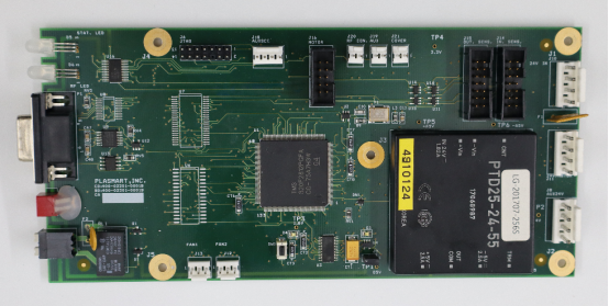
A practical example of QFP use can be found in microcontroller chips, such as the ATmega328P used in Arduino boards. The ATmega328P comes in a 32-pin QFP package, which is small enough to fit into a variety of devices but also provides enough pins to handle all the necessary connections for a microcontroller. Its QFP design makes it easy for engineers to solder and test during development, and it works well in consumer products like DIY electronics kits.
Core Design Features of QFP
Lead Configuration and Design
Description of Gull-Wing Leads and Their Orientation
One of the key features of the QFP is its gull-wing leads. These leads are thin metal pins that extend outward from each of the four sides of the flat package. They are bent into a shape that resembles a bird's wings, which is where the name "gull-wing" comes from. This design allows the leads to connect to the circuit board without passing through it, making the QFP a surface-mount package.
The leads are typically soldered to the surface of a printed circuit board (PCB), which is a common method in modern electronics. This configuration is preferred for its ease of handling during manufacturing and assembly.
How Lead Configuration Impacts Installation and Inspection
The gull-wing lead configuration has several benefits for installation and inspection:
1. Ease of Soldering: Since the leads extend out from the package, they are easy to access for automated machines and even hand-soldering during prototype assembly.
2. Visual Inspection: The outward-bent leads are clearly visible, making it simple to inspect the solder joints for any defects such as poor connections or cold solder joints. This is particularly helpful during quality control processes.
3. Alignment during Installation: The leads’ shape ensures that the component can be easily placed onto a PCB and aligned correctly by automated pick-and-place machines.
This design is a key reason why QFPs are widely used in industries that require precision, such as consumer electronics, automotive systems, and industrial machinery.
Size and Pin Count Variability
Breakdown of Available QFP Sizes (32–200 Pins)
QFPs are versatile in terms of the number of pins they can accommodate. The most common pin count ranges from 32 pins to 200 pins, with 100-pin and 144-pin variations being especially popular. The number of pins in a QFP package determines the types of connections it can make to the PCB, and it is often chosen based on the complexity of the chip and the device it is powering.
For example, a 32-pin QFP might be used for simpler microcontrollers, while a 144-pin QFP could be used for more complex processors or system-on-chip (SoC) designs in consumer electronics like smartphones or televisions.
Relationship Between Pin Count and Design Complexity in Consumer and Industrial Devices
The pin count directly influences the complexity of the electronic design. Chips with fewer pins, such as those with 32 or 48 pins, are typically used in simpler devices like basic microcontrollers or audio chips. These devices often perform straightforward functions and require fewer connections to the circuit board.
In contrast, higher pin counts (100–200 pins) are common in devices that require more processing power or functionality, such as automotive infotainment systems, industrial sensors, and high-performance microprocessors. The more pins a chip has, the more complex the device's circuitry becomes, allowing for additional features like increased memory, faster processing speeds, or more input/output (I/O) connections.
Real-life example: The ATmega328P used in Arduino microcontrollers is available in a 32-pin QFP. It’s ideal for simpler, low-cost electronic projects. Meanwhile, a 144-pin QFP might be used for more complex devices like a digital signal processor (DSP) in a sound system.
Profile and Thickness
Average Thickness Range (1.5mm–3mm)
QFP packages are designed to be relatively thin, with an average thickness range of 1.5mm to 3mm. This compact profile is especially important in modern electronics, where devices need to be slim and lightweight, especially for consumer products like TVs, laptops, and smartphones.
The low profile of the QFP helps it fit into compact spaces without significantly increasing the overall size of the device. This is important for maintaining the sleek design of modern electronics while ensuring the internal components remain functional and efficient.
How the Flat Profile Makes QFP Suitable for Slim Devices
The flat profile of a QFP package makes it ideal for slim, space-constrained devices. Because the leads are on the sides and not underneath the package (as with other types of chips), QFPs can be easily mounted on the surface of a PCB without taking up too much vertical space. This is especially useful in devices that need to be as thin as possible, such as smartphones and flat-screen televisions, where internal space is at a premium.
A QFP’s flat design contrasts with other package types, like BGAs, which may require more vertical space due to their bottom-mounted leads. For slim, lightweight products, QFP is often the best choice for efficient use of space.
Lead Pitch and Spacing
Common Lead Pitch Sizes (0.4mm–0.8mm)
The lead pitch refers to the distance between the centers of two adjacent leads on a QFP. Common lead pitch sizes for QFPs range from 0.4mm to 0.8mm. A smaller pitch (0.4mm) allows for more pins in a compact space, which is useful for devices that need a higher pin count in a smaller footprint. Conversely, a larger pitch (0.8mm) makes soldering and assembly easier, but it results in fewer pins being placed on the package.
The choice of lead pitch depends on the specific needs of the device and the manufacturing process. For example, 0.4mm pitch is typically used in high-density applications, like processors in smartphones, where maximizing the number of connections is essential. A 0.8mm pitch is more commonly found in less complex devices like audio chips or simpler microcontrollers.
Impact of Lead Spacing on Manufacturing and Assembly
The spacing between leads directly impacts both manufacturing and assembly processes:
1. Small Pitch (0.4mm): Devices with a smaller lead pitch require precise handling during both assembly and soldering. Specialized equipment and careful quality control are necessary to avoid solder bridges (when solder connects two leads), which could cause circuit malfunctions.
2. Larger Pitch (0.8mm): A larger lead pitch simplifies the manufacturing process. It reduces the likelihood of errors during soldering and allows for easier inspection of the leads. This is particularly important in industries where high-volume, reliable production is necessary.
For example, a 0.8mm pitch QFP might be used in consumer electronics like printers or TVs, where the device doesn't require as many pins but still needs reliable performance and easier assembly. On the other hand, 0.4mm pitch QFPs are ideal for high-density chips used in smartphones or advanced automotive systems.
QFP Manufacturing and Assembly
Automated Assembly and SMT
How QFP Fits Within Automated Pick-and-Place Machines
QFP packages are designed to be easily handled by automated pick-and-place machines. These machines are used in modern manufacturing to quickly and accurately place components like QFPs onto a PCB. The gull-wing leads on a QFP make it easy for the machine’s suction arms to pick up the component, align it properly, and place it onto the board.
The machine’s precision ensures that the QFP is placed exactly in the right spot on the PCB, which is critical for ensuring that all the electrical connections between the leads and the PCB are correct. Automated systems can place QFP packages at a much higher speed than human workers, making the assembly process more efficient and cost-effective.
Soldering and Mounting Process for QFP Packages
Once the QFP is placed on the PCB, the soldering process begins. In automated assembly, reflow soldering is commonly used. Here’s how it works:
1. Solder Paste Application: First, solder paste (a mixture of tiny metal balls and flux) is applied to the PCB in areas where the QFP’s leads will make contact.
2. Placement: The pick-and-place machine places the QFP on the PCB, aligning it with the paste.
3. Reflow Oven: The board is then passed through a reflow oven, where heat melts the solder paste, forming a solid electrical connection between the leads and the PCB.
4. Inspection: After soldering, automated machines or human inspectors check for any soldering defects, such as bridges or cold joints, using techniques like X-ray inspection or optical inspection.
5. This process ensures that QFPs are securely mounted and electrically connected, ready for further testing or integration into finished devices.
Hand Soldering Capabilities for Prototyping
Why QFP is Suitable for Small-Batch or Prototyping Use
While automated systems are perfect for mass production, QFP packages are also well-suited for small-batch manufacturing or prototyping. For engineers working on prototypes or small runs, QFPs offer flexibility. The gull-wing leads are easy to access, making manual soldering simpler compared to other packages, like BGAs, where leads are hidden underneath the component.
Prototyping often requires custom assembly, which may not be feasible with fully automated systems. QFP’s design allows engineers to quickly assemble and test their designs without needing expensive automated equipment. This makes it an ideal choice for startups, hobbyists, and engineers working on early-stage projects.
Techniques for Hand-Soldering QFP Leads Effectively
Hand-soldering a QFP requires some skill and patience, but it can be done with the right tools. Here are key techniques for effective hand-soldering:
1. Use a Fine-Tip Soldering Iron: A soldering iron with a fine, sharp tip allows for precise control over the heat application and minimizes the risk of damaging surrounding components.
2. Soldering the Leads: Begin by applying solder to one corner lead to hold the QFP in place. Then, move on to solder the remaining leads one by one, ensuring each lead is heated properly.
3. Flux for Better Soldering: Use soldering flux to clean the pads and leads before soldering. This helps the solder flow smoothly and prevents bridges or poor connections.
4. Inspecting the Joints: After soldering, inspect the leads using a magnifying glass or microscope to ensure clean, solid joints without bridges. You can also use solder wick to remove excess solder or fix any mistakes.
With these techniques, hand-soldering a QFP can be efficient and effective, making it an excellent option for small-scale projects or prototypes.
Challenges in Assembly
Potential Issues with Lead Damage During Handling
One of the main challenges in the assembly of QFPs is lead damage. The gull-wing leads are relatively thin and can easily be bent or deformed if not handled carefully. This can occur during the pick-and-place process, transportation, or even during manual soldering. Bent or damaged leads can cause poor electrical connections, leading to device failure.
To avoid lead damage, manufacturers and engineers must handle QFP packages with care. Using tools such as tweezers or vacuum pickups can help prevent unnecessary stress on the leads. Additionally, proper packaging and protective handling during transportation are important to maintain the integrity of the component.
Precautions to Avoid Lead Bending or Other Mechanical Failures
Several precautions can help prevent lead bending or other mechanical failures during assembly:
Use of Anti-Static and Protective Packaging: QFP components should be stored and transported in protective packaging that prevents physical damage and exposure to static electricity, which can also harm the leads.
Proper Handling: During manual assembly, engineers should handle QFPs gently and use tools designed to grip the component without putting pressure on the leads. This reduces the risk of bending or breaking them.
Alignment During Assembly: For automated pick-and-place machines, proper calibration is essential to ensure that the machine correctly aligns the component without applying excessive force that might bend the leads.
Use of Soldering Jigs: When hand-soldering, consider using soldering jigs to hold the QFP in place while you work, preventing it from moving or shifting, which can cause stress on the leads.
By following these precautions, manufacturers and engineers can ensure that the QFP leads stay intact and functional, contributing to the overall quality and reliability of the final product.
Pros and Cons of QFP Packaging
Advantages of QFP
Ease of Inspection: Visible Leads, Easy to Check Solder Joints
One of the key advantages of QFP packages is the visibility of the leads. The gull-wing design of the leads means they extend outward from all four sides of the package, making them easy to inspect. This feature allows engineers to check solder joints visually, ensuring that the connections are solid and free from defects like solder bridges or cold solder joints. In contrast, packages like BGAs have leads underneath the package, making them harder to inspect without advanced tools like X-rays.
The ease of inspection significantly reduces the time spent on quality control and helps prevent production errors, improving the overall reliability of the product. This is especially important in industries like consumer electronics, where high-quality standards are critical.
Versatile Pin Count: Ideal for Microcontrollers to Mid-Range SoCs
QFP packages are highly versatile in terms of the number of pins they can accommodate, typically ranging from 32 to 200 pins. This makes them suitable for a wide variety of devices, from simpler microcontrollers (such as those used in hobby electronics) to more complex SoCs found in smartphones, computers, and industrial systems.
The flexibility in pin count allows designers to choose a QFP package based on the specific needs of the device, providing a cost-effective solution for both low- and medium-complexity electronics. For instance, a 32-pin QFP might be used in a simple microcontroller, while a 144-pin QFP could power a more complex SoC in an automotive infotainment system.
Cost Efficiency: Affordable Compared to BGA and LCC
When compared to other packaging options like BGAs or LCCs, QFP packages are generally more affordable. The production process for QFPs is less complex, and the materials used are cheaper, which helps reduce the overall cost of manufacturing. This makes QFP a cost-effective choice for devices that require moderate complexity without the need for high-density connections.
For example, QFPs are often used in consumer electronics like TVs or printers, where affordability is important, but the need for extreme performance and high-density interconnections is not as critical as in high-end computing devices.
Prototyping Friendliness: Hand-Soldering Capabilities for Small Runs
QFP packages are ideal for small-batch production and prototyping because they can be hand-soldered with relative ease. This makes them a great option for engineers and hobbyists who are working on early-stage designs or limited runs. Unlike more advanced packaging types such as BGAs, which require specialized equipment and techniques for soldering, QFP’s gull-wing leads are easily accessible with a standard soldering iron.
For example, in an electronics project or a DIY kit, a designer might use a 32-pin QFP for a microcontroller. The leads are easy to solder manually, allowing for quick testing and adjustments before moving on to mass production.
Disadvantages of QFP
Solder Bridging Risk: Challenges with Fine-Pitch Leads
One of the main challenges of using QFP packages, particularly those with fine-pitch leads (0.4mm spacing), is the risk of solder bridging. Solder bridges occur when solder unintentionally connects two adjacent leads, which can short-circuit the device and cause malfunctions. Fine-pitch leads, which are commonly found in high-pin-count QFPs, are more prone to this issue because the leads are very close together.
Manufacturers can mitigate this risk by using precise solder paste application and reflow soldering techniques, which help ensure the solder stays where it's needed. In some cases, manual inspection or automated optical inspection systems are used to detect any solder bridges before the device is finalized.
Lead Damage: Vulnerability to Physical Bending and Breakage
QFP packages, especially those with gull-wing leads, are vulnerable to lead damage during handling. The leads can be bent, deformed, or even broken if not handled properly. This is particularly a concern during the pick-and-place process or during transport to assembly lines. If the leads are damaged, it can result in poor electrical connections and may require rework or replacement of the component.
To minimize the risk of lead damage, automated handling systems are used in mass production to reduce human error. For smaller batches or prototypes, careful handling is required, and tools like vacuum pick-up systems or tweezers should be used to avoid putting stress on the leads.
Footprint Size: Larger Area Required Compared to BGA
While QFP packages are versatile, they do require a larger footprint compared to BGAs. A 200-pin QFP, for example, may require a 25mm x 25mm area on a PCB, while a BGA with the same number of pins can often be smaller due to its more compact design, where the leads are located under the package.
This larger footprint can be a disadvantage when trying to save space on a densely packed PCB, especially in smaller, portable devices like smartphones. However, QFP’s larger footprint also provides benefits, such as easier accessibility to the leads for inspection and repair.
Heat Dissipation Challenges: Insufficient Heat Transfer for High-Power Chips
Another drawback of the QFP package is its heat dissipation capabilities. The leads of a QFP are relatively thin and do not transfer heat as effectively as other package types like BGAs or LCCs. This can be a problem for high-power chips (those consuming more than 5W of power) that generate significant heat during operation. Without adequate cooling, high-power chips in QFP packages may overheat, leading to reduced performance or potential failure.
To address this issue, additional thermal management solutions such as heat sinks, thermal vias, or fan systems may be required to prevent overheating. In applications where heat dissipation is a concern, designers might choose other package types that offer better thermal performance.
Best Practices for Handling and Soldering QFP Packages
Preventing Lead Damage
Proper Handling Techniques to Avoid Physical Damage to Leads
QFP packages are delicate, and their gull-wing leads can easily be bent or damaged if not handled properly. To avoid this, it's important to handle QFP components carefully during the assembly process. The leads should never be touched directly with bare hands, as this can cause static discharge or physical damage. Always use anti-static mats and tools when working with QFPs to prevent any damage.
For automated assembly, pick-and-place machines are designed to handle QFPs with precision. However, for manual handling or small-batch assembly, use vacuum pick-up tools or tweezers specifically designed for surface-mount components. These tools apply gentle pressure and reduce the risk of damaging the leads.
Use of Protective Tools During Assembly
During assembly, the use of protective tools can further prevent lead damage. For example, using soldering jigs or holding fixtures to secure the QFP in place during soldering can prevent unnecessary stress on the leads. These tools help hold the component steady, ensuring that it doesn’t shift during soldering or cause bending of the delicate gull-wing leads.
In mass production, automated handling systems that control the movement of QFPs are essential. For smaller-scale operations or prototypes, using soft-touch forceps and vacuum-based placement tools will also reduce the risk of mishandling the leads.
Avoiding Soldering Issues
Techniques to Prevent Solder Bridging and Ensure Reliable Connections
Solder bridging occurs when excess solder connects two adjacent leads, creating an unwanted electrical connection that can lead to device malfunction. To avoid this, it is crucial to apply the right amount of solder during the process. Here are a few tips:
1. Use of Solder Paste: When applying solder paste, make sure it's precisely placed on the PCB pads. Too much paste can cause bridges, while too little may lead to weak connections.
2. Fine-Tip Soldering Iron: A fine-tip soldering iron allows for precise control of solder application, reducing the risk of applying excess solder.
3. Reflow Soldering: Using reflow soldering is the most effective way to avoid solder bridges. The controlled heat allows the solder to melt evenly, ensuring that only the leads and pads make a secure connection.
4. Inspection: After soldering, use magnification tools such as a magnifying glass or microscope to inspect the solder joints. Automated optical inspection systems can also be used for more precise checks.
These techniques ensure that the leads are properly soldered without creating bridges that could damage the circuit.
Recommended Equipment and Materials for Precise Soldering
To achieve high-quality soldering on QFPs, using the right equipment is essential. Key tools and materials include:
Fine-tip soldering iron: For precise control over the soldering process.
Soldering flux: This helps the solder flow smoothly and adhere to the pads without causing defects.
Solder paste: Essential for accurate application of solder during reflow soldering.
Solder wick (desoldering braid): For cleaning up excess solder or fixing mistakes such as solder bridges.
Magnifying equipment: Helps in inspecting the leads and solder joints closely to ensure high-quality connections.
By using these tools, soldering becomes more efficient and reduces the likelihood of common issues like solder bridging or weak connections.
Maximizing Heat Dissipation
Suggested Cooling Solutions for Higher-Power QFP Chips
QFP packages, particularly those used in high-power applications (e.g., chips consuming more than 5 watts), may generate significant heat during operation. Without proper cooling, the chip can overheat, affecting performance and possibly leading to failure. To address this, additional cooling solutions are needed. Some of the most common solutions include:
1. Thermal Vias: These are small holes in the PCB that allow heat to travel away from the chip to other layers of the board, improving overall heat distribution.
2. Thermal Pads or Conductive Tape: These materials can be placed between the QFP package and the PCB to help draw heat away from the chip.
3. Fans or Forced Air Cooling: In cases where the device operates at high power for extended periods, installing a fan near the device can provide additional cooling.
Use of Heat Sinks or Other Thermal Management Methods
For high-performance QFP chips, heat sinks can be attached to the top of the package to absorb and dissipate heat. Heat sinks are metal components designed with fins that increase the surface area for heat dissipation. By attaching a heat sink to the QFP, the device can remain cool even under heavy loads, ensuring it continues to perform optimally.
Other methods of thermal management include:
Active cooling: This involves using fans or liquid cooling systems to lower temperatures in environments where heat buildup is a significant concern.
Thermal interface materials (TIMs): These are special materials used between the QFP package and the heat sink to improve thermal contact and ensure better heat transfer.
By incorporating these heat dissipation strategies, you can prevent overheating, extend the lifespan of the QFP package, and ensure that the chip operates efficiently in demanding applications.

Comparison of QFP with Other Packaging Types
QFP vs. BGA
Key Differences in Pin Count, Footprint, and Soldering Complexity
When comparing QFP and BGA, the most noticeable differences lie in pin count, footprint, and soldering complexity.
Pin Count: While both QFP and BGA can support a range of pins, QFPs are more common in devices with moderate pin counts, typically ranging from 32 to 200 pins. BGAs, on the other hand, are used for chips requiring higher pin densities, often exceeding 200 pins.
Footprint: A key difference is the footprint size. BGAs are more compact due to their leads being placed underneath the package, which allows for a smaller PCB space. QFP packages, with leads on all four sides, generally require more surface area for the same pin count. For example, a 200-pin QFP requires a 25mm x 25mm area, whereas a 200-pin BGA would likely take up a smaller footprint.
Soldering Complexity: QFPs are easier to solder compared to BGAs, especially in manual assembly. The gull-wing leads on a QFP are accessible for hand-soldering, making them suitable for prototyping and low-volume production. In contrast, BGAs have hidden leads underneath the package, making soldering more complex and requiring specialized equipment like X-ray inspection or reflow soldering with precise control.
Advantages of QFP in Prototyping vs. the Higher Performance of BGA
For prototyping and small-scale production, QFPs are often the better choice. Their gull-wing leads make them easier to handle and inspect, which is important when engineers need to quickly test and modify their designs. The ease of hand-soldering and visual inspection of QFP packages saves time and reduces the cost of prototypes.
On the other hand, BGAs are designed for high-performance applications. They offer superior electrical performance due to their more compact design and the ability to handle higher pin counts in a smaller space. BGAs are typically used in products that demand more processing power, such as high-end computers, smartphones, and network equipment.
Example: A microcontroller with a 32-pin QFP might be used in a basic DIY project or a small consumer product, where ease of assembly and low cost are essential. For a smartphone’s CPU, a BGA package would be preferred because of its ability to handle higher performance in a smaller size.
QFP vs. LCC
Discussion of Lead Configuration Differences and Their Impact on Assembly
The primary difference between QFP and LCC lies in their lead configuration.
QFP packages have gull-wing leads that extend outward from all four sides of the package. These leads make the component easy to handle, inspect, and solder using SMT. The outward leads are accessible, which makes QFP ideal for prototyping and applications requiring visual inspection and manual soldering.
LCC, on the other hand, does not have leads. Instead, the electrical connections are made through pads on the underside of the package. LCC packages are leadless, which means they have no outward leads, and this makes them harder to handle and inspect compared to QFPs. Because of this, LCCs are generally better suited for high-volume, automated manufacturing where precision soldering techniques are required.
The lack of leads in LCC packages results in a more compact design, which is beneficial for space-constrained applications. However, this also makes LCCs more challenging to work with manually, as the package must be attached directly to the PCB with solder paste using automated equipment.
When to Choose QFP Over LCC in Different Design Scenarios
Choosing between QFP and LCC depends largely on the specific requirements of the device being designed:
Choose QFP if manual assembly or prototyping is necessary. The gull-wing leads are easy to handle, inspect, and solder, making them ideal for low-volume production or when quick changes to the design are needed.
Choose LCC if the design needs a compact package with no visible leads and will be produced in high volumes. LCC packages can offer smaller footprints and better performance for densely packed PCBs, but they are more challenging to work with in small-scale assembly.
Example: For a consumer product like a TV remote control where prototyping and manual soldering may be required, a QFP package is often the better choice. For a smartphone or high-end computer motherboard where space is at a premium and automated assembly is the focus, an LCC package may be preferred.
Comparison Table: QFP vs. BGA vs. LCC
Feature QFP BGA LCC Lead Configuration Gull-wing leads (visible) Leads underneath (hidden) No leads (pads on bottom) Footprint Larger footprint (surface mount) Smaller footprint (compact) Smallest footprint (compact) Soldering Complexity Easy to hand-solder, visual inspection Requires X-ray, specialized equipment Requires precise automated assembly Prototyping Friendliness Ideal for prototyping and low volumes Not ideal for prototyping Difficult for prototyping Performance Suitable for moderate applications High performance, high-density I/O Suitable for high-volume, space-constrained applications Cost Relatively low cost Higher cost due to complexity Typically lower cost, high-volume Inspection Easy visual inspection Difficult to inspect without X-ray No easy inspection, automated required
Conclusion
Choosing the right packaging type for your electronic components—whether it's QFP, BGA, or LCC—depends on the specific needs of your project, such as performance, footprint, and assembly requirements. Each package has its strengths, and understanding these can help ensure optimal performance and cost efficiency. If you’re looking for reliable PCB manufacturing and assembly solutions, PCBMASTER is a trusted provider, offering high-quality PCBs that cater to various packaging types, including QFP and beyond. With their expertise, you can bring your designs to life with precision and efficiency.
FAQs
What is the difference between QFP and BGA packaging?
The QFP and BGA are both surface-mount packages but differ significantly in design and application. In a QFP, the component has gull-wing leads on all four sides, which extend outward from the body of the package. These leads are visible, making it easier for manual assembly and visual inspection. On the other hand, BGA packages use solder balls underneath the component, which provide the electrical connections. This design allows for a much higher pin density and smaller footprint, making BGAs ideal for high-performance devices like CPUs and GPUs, where space and high pin counts are critical. However, BGA soldering requires more specialized equipment, such as X-ray inspection or reflow soldering, due to the hidden leads. In contrast, QFPs are easier to handle and more accessible for manual soldering, making them ideal for prototyping or low-volume production.
Can QFP be used for high-performance processors?
While QFP packages are versatile, they are typically not ideal for high-performance processors like those found in high-end computing or gaming systems. QFP packages have a relatively large footprint and a limited ability to dissipate heat due to the design of their leads, which can cause overheating in processors that generate a lot of heat during operation. For high-power chips, such as multi-core processors or graphics processing units (GPUs), packages like BGAs are preferred because they provide a more efficient thermal path through their underside leads and can accommodate more pins in a smaller space. High-performance processors often require more sophisticated heat sinks or thermal management systems, which are better supported by BGA or LCC packages. In contrast, QFPs are more suitable for chips with moderate performance demands that don’t generate significant heat.
How can I ensure reliable solder joints on a QFP package?
Ensuring reliable solder joints on a QFP package requires attention to detail during the soldering process. Here are some key tips:
Use precise soldering techniques: It’s essential to use a fine-tip soldering iron to precisely apply solder to each lead. This allows you to control the amount of solder used and avoid excessive solder, which can lead to bridging (where solder connects two adjacent leads unintentionally).
Avoid over-soldering: Over-soldering can result in a messy joint, making it difficult to inspect and increasing the risk of solder bridging. Only enough solder should be applied to make a strong electrical connection between the lead and the PCB pad.
Consistent paste application: When using solder paste, make sure it is applied evenly and in the right amount. Too much solder paste can lead to excess solder flow, which increases the risk of short circuits. Reflow soldering can help with even solder distribution, ensuring that each lead is properly soldered.
Inspect solder joints: After soldering, visually inspect the joints under magnification to ensure there are no defects like cold joints (weak solder connections) or bridges.
By following these steps, you can ensure that your QFP package is properly soldered, improving its reliability and performance.
What are the best tools for hand-soldering QFP?
To hand-solder QFP packages accurately, you’ll need the following tools:
Fine-tip soldering iron: A fine-tip soldering iron allows for precision when working with the small leads of a QFP package. The fine tip ensures that only the necessary amount of solder is applied to each lead, reducing the risk of bridging and making it easier to work with fine-pitch QFPs.
Solder flux: Flux helps the solder to flow more easily and adhere to the lead and PCB pad, ensuring a strong electrical connection. It also prevents oxidation and helps the solder to form smooth, shiny joints.
Magnifying tool: Since QFP packages often have small pins, it’s important to use a magnifying tool such as a magnifying glass or microscope. This will help you inspect each joint carefully and make sure there are no soldering defects like bridges or cold joints.
Solder wick (desoldering braid): If you need to remove excess solder or correct mistakes, solder wick is an excellent tool to soak up the unwanted solder without damaging the leads.
By using these tools, you can achieve precise and reliable soldering on QFP packages.
Why are QFPs more commonly used in consumer electronics than in high-performance computing?
QFP packages are more commonly found in consumer electronics like TVs, printers, and audio systems because they offer an excellent balance of cost, size, and ease of assembly. These products typically use moderate-performance chips that don’t require the high pin densities or advanced heat dissipation features offered by packages like BGA. QFPs are relatively inexpensive to manufacture and easy to assemble, making them ideal for mass production of consumer products. They can also be hand-soldered, which is a great advantage in small-batch or prototyping situations, further reducing manufacturing costs.
In contrast, high-performance computing devices, like servers and gaming consoles, require greater pin density and more effective thermal management. As a result, packages like BGA or LCC are typically chosen for these applications, where performance and space constraints are more critical.
Author Bio
Hi, I'm Carol, the Overseas Marketing Manager at PCBMASTER, where I focus on expanding international markets and researching PCB and PCBA solutions. Since 2020, I've been deeply involved in helping our company collaborate with global clients, addressing their technical and production needs in the PCB and PCBA sectors. Over these years, I've gained extensive experience and developed a deeper understanding of industry trends, challenges, and technological innovations.
Outside of work, I'm passionate about writing and enjoy sharing industry insights, market developments, and practical tips through my blog. I hope my posts can help you better understand the PCB and PCBA industries and maybe even offer some valuable takeaways. Of course, if you have any thoughts or questions, feel free to leave a comment below—I'd love to hear from you and discuss further!

