


Comprehensive Guide to BGA Package Design and Soldering Process in PCB Manufacturing
In today’s electronics landscape, devices are shrinking while performance demands keep rising. High-density chips and memory modules need packaging that can handle more connections in less space, maintain reliable electrical performance, and manage heat effectively. Among the options available, BGA (Ball Grid Array) stands out as a solution that meets these challenges, enabling faster, more compact, and more reliable circuits. Its unique structure and capabilities have made it a cornerstone in modern PCB design, from consumer electronics to high-speed computing systems.
What Is BGA (Ball Grid Array) Packaging?
Definition and Structure of BGA
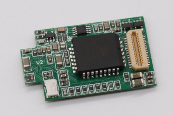
A Ball Grid Array (BGA) is a type of surface-mount chip packaging used to connect integrated circuits (ICs) to printed circuit boards (PCBs). Instead of using traditional leads or pins, BGA packages use a grid of tiny solder balls arranged on the underside of the chip. These solder balls act as both the electrical connection and mechanical support between the chip and the PCB.
Each solder ball corresponds to a circuit node on the chip, and when heated during the reflow soldering process, it melts to form a reliable bond with the matching PCB pad. Because the solder joints are distributed evenly across the entire bottom surface, BGA provides lower electrical resistance and shorter signal paths, improving both signal integrity and high-speed performance.
From a mechanical perspective, BGA’s evenly spaced solder balls reduce stress on individual joints, increasing durability and resistance to thermal cycling. The structure also offers superior heat dissipation, as heat can spread through the solder balls and the PCB substrate, minimizing the risk of overheating in dense electronic systems.
BGA packaging is widely adopted in memory modules (such as DDR and flash memory), motherboard chipsets, and high-performance processors. Its compact design enables manufacturers to fit more functionality into smaller footprints—an essential advantage for smartphones, laptops, and IoT devices, where miniaturization is critical.
Comparison Between BGA and TSOP Packages
BGA and TSOP (Thin Small Outline Package) are both surface-mount technologies, but their structural design and performance characteristics differ significantly.
1. Structural Differences and Space Efficiency
TSOP packages have leads that extend from the sides of the chip and connect to PCB pads, which limits how closely they can be spaced. In contrast, BGA places solder balls in a two-dimensional grid underneath the package, allowing for hundreds or even thousands of interconnections within the same area.
Because of this grid layout, BGA offers higher pin density and smaller footprint compared to TSOP—ideal for high-pin-count ICs where board space is limited.
2. Electrical and Thermal Performance
BGA connections are shorter and more uniform, reducing parasitic inductance and resistance that often degrade high-frequency signals in TSOP packages. This results in faster signal transmission and improved power integrity.
Thermally, BGA packages outperform TSOP due to better heat conduction through the solder balls and substrate, which helps maintain stable operation even under heavy computational loads.
3. Typical Applications and Use Cases
BGA: Used in CPUs, GPUs, DDR memory, and high-speed communication ICs where high performance and thermal stability are required.
TSOP: Still preferred for lower-cost or lower-density memory devices, such as older-generation flash memory or consumer-grade controllers, where simplicity and lower assembly cost are prioritized.
In summary, while TSOP remains practical for moderate-performance applications, BGA is the superior choice for advanced, high-density, and thermally demanding electronics. Its balance of miniaturization, electrical efficiency, and mechanical reliability makes it a cornerstone of modern PCB assembly and semiconductor packaging.
Key Considerations in BGA Pad and Trace Design
Routing Between BGA Pads
When designing PCB layouts for Ball Grid Array (BGA) components, routing between pads becomes increasingly challenging as pad pitch decreases below 10 mil (0.254 mm). At such fine spacing, most PCB manufacturers cannot guarantee the minimum trace width and clearance required to place a reliable signal route between adjacent pads.
Attempting to route traces between pads that are too close can result in solder bridging, short circuits, or incomplete etching during fabrication. Some designers may try to reduce the pad size to create additional space, but this introduces new problems—smaller pads reduce solder contact area, which can lead to misalignment and weaker solder joints during assembly.
Best practices for BGA pad routing focus on balancing electrical performance and manufacturability:
Avoid routing between pads when the pitch is below 10 mil.
Use microvias or via-in-pad structures to escape dense BGA layouts.
Maintain consistent pad-to-pad clearance and mask-defined pads to improve alignment accuracy.
Collaborate closely with the PCB manufacturer to confirm the minimum trace/space capability before finalizing the design.
By adhering to these guidelines, designers can prevent production issues and ensure high soldering reliability in dense BGA layouts.
Via-in-Pad Design and Resin Plugging
In high-density PCB designs, engineers often use via-in-pad technology, where a drilled via hole is placed directly inside the BGA pad. This allows traces to connect vertically through inner or bottom layers instead of routing between pads on the same layer. Via-in-pad is essential for fine-pitch BGA components where traditional fan-out routing is impossible.
However, an unplugged via creates a serious risk of solder wicking—the molten solder can flow into the hole during reflow, leaving insufficient solder on the pad and resulting in open circuits or weak joints. To prevent this, the via must be resin plugged and plated over with copper to form a flat, solderable surface.
This resin plugging and copper filling process:
Ensures consistent solder volume for each pad.
Improves planarity, critical for precise BGA placement.
Increases assembly yield by eliminating hidden solder voids or shorts.
Proper via-in-pad design significantly enhances signal integrity and mechanical strength, making it a preferred choice for high-speed and multilayer PCBs used in computing, telecom, and automotive systems.
Through-Hole Plugging in BGA Areas
In BGA regions, through-hole vias can create reliability risks during Surface Mount Technology (SMT) assembly. Open vias located beneath BGA pads can trap contaminants, cause solder leakage, or allow solder to wick to the opposite side, creating unwanted shorts.
To prevent these problems, designers use via plugging—filling the hole with either ink or resin to seal it before soldering.
Ink plugging (solder mask plugging): A cost-effective method used mainly in prototype or low-density boards. It provides basic protection but may not be suitable for fine-pitch BGAs.
Resin plugging: Involves filling the via with epoxy resin and plating it flat, offering better durability and moisture resistance for mass production or high-reliability boards.
Choosing between these two methods depends on the cost-performance balance:
Ink plugging = lower cost, moderate reliability.
Resin plugging = higher cost, maximum reliability and lifespan.
For critical products such as servers, automotive ECUs, or aerospace boards, resin-filled vias are strongly recommended to ensure long-term stability under thermal and mechanical stress.
HDI and Via-in-Pad Design for Fine-Pitch BGAs
As devices become thinner and more powerful, fine-pitch BGA packages (≤0.5 mm pitch) require HDI (High-Density Interconnect) technology to maintain both electrical performance and manufacturability. In such boards, it’s impossible to route traces through traditional layers without using blind vias, buried vias, or stacked microvias.
These HDI techniques allow signals to escape from the inner pads of a BGA without taking up additional surface area. For example:
Blind vias connect outer layers to nearby inner layers.
Buried vias connect internal layers without reaching the surface.
Stacked microvias provide high-density vertical connections for ultra-compact designs.
Design tips for HDI BGA layouts:
Keep microvia aspect ratios ≤1:1 to ensure plating quality.
Use resin-filled via-in-pad for consistent solder joints.
Maintain uniform via alignment to prevent layer shifting during lamination.
Simulate signal integrity (SI) early in the design to avoid impedance mismatches caused by microvia stubs or layer transitions.
By applying HDI and via-in-pad design principles, engineers can successfully integrate high-pin-count BGAs into modern smartphones, wearables, and networking devices while maintaining signal fidelity, reliability, and manufacturability.
Step-by-Step BGA Soldering Process
Solder Paste Printing
The first step in the BGA (Ball Grid Array) soldering process is solder paste printing—a critical stage that directly affects the quality of every subsequent step. Solder paste is a mixture of fine solder particles and flux used to form the electrical and mechanical connection between the BGA pads and the PCB. Its main function is to provide precise solder volume and placement, ensuring that each solder ball on the BGA aligns correctly with its corresponding pad.
The stencil design, paste thickness, and printing pressure all play a major role in achieving consistent deposition. A properly designed stencil—usually made of stainless steel—controls how much paste is applied to each pad. Typical stencil thickness for BGA ranges between 0.10 mm and 0.15 mm, depending on pad size and pitch. Uniform pressure during the squeegee pass ensures even paste distribution across all apertures.
Common issues during this stage include:
Insufficient paste → causes incomplete solder joints or open circuits.
Excess paste → may lead to solder bridging or short circuits.
Uneven deposition → results in inconsistent joint height, increasing stress after reflow.
For reliable results, the paste should be inspected under magnification, and stencil cleaning frequency should be adjusted according to production conditions to maintain consistent print quality.
Component Placement
After solder paste application, the BGA component must be accurately placed on the PCB. Because the solder balls serve as both interconnects and alignment points, even slight placement errors can lead to misalignment, tilting, or open joints after reflow.
Modern SMT production lines use two types of pick-and-place machines:
High-speed placement machines – optimized for small, lightweight components such as resistors and capacitors.
General-purpose (precision) placement machines – designed for larger and more complex packages like BGAs, QFNs, and QFPs, where micron-level accuracy is required.
Typical placement tolerance for BGAs is within ±50 μm, depending on the package size and pitch. To maintain this precision, optical vision systems are used to identify fiducial marks on both the PCB and the component before alignment.
Accurate placement ensures that each solder ball lands on its intended pad, allowing surface tension during reflow to self-align the component perfectly. Poor placement, on the other hand, often leads to bridging or opens that cannot be corrected later in the process.
Reflow Soldering Process
Reflow soldering is the stage where mechanical and electrical connections between the BGA and PCB are permanently formed. During this process, the assembly passes through a temperature-controlled oven that gradually heats, melts, and then solidifies the solder paste.
The process is typically divided into four main temperature zones:
1. Preheat Zone – gradually warms the PCB to prevent thermal shock.
2. Soak Zone – stabilizes the temperature across the board and activates the flux.
3. Reflow Zone – the solder reaches its liquidus temperature (around 217°C for lead-free solder), forming the actual solder joints.
4. Cooling Zone – solidifies the solder, ensuring a strong metallurgical bond.
Common reflow defects include:
Cold solder joints (caused by insufficient temperature or short dwell time).
Tombstoning (caused by uneven heating or surface tension imbalance).
Solder balls or bridging (caused by excessive paste or rapid heating).
To prevent these, engineers must carefully control the reflow temperature profile, match it to the PCB’s thermal capacity, and ensure even airflow distribution inside the oven.
X-Ray Inspection in BGA Assembly
Because the solder joints of a BGA are hidden beneath the package, visual inspection is impossible. This is why X-ray inspection is the standard method for verifying solder quality in BGA assemblies. X-ray systems can penetrate the package and display detailed images of the solder balls and pads beneath the chip, allowing engineers to identify hidden defects.
X-ray imaging helps detect:
Voids – trapped air pockets inside solder joints.
Bridging – solder connecting two adjacent balls.
Insufficient solder or missing joints – where a ball failed to wet properly.
Misalignment – where balls are offset from their pads.
Compared to optical inspection, X-ray offers unmatched visibility for hidden interconnects but comes with higher equipment cost and slower throughput. However, for BGAs and other area-array packages, X-ray inspection remains the most reliable method for ensuring assembly integrity and long-term reliability.
In high-volume production, automated 2D and 3D X-ray systems are often integrated into the SMT line, providing real-time analysis of each board. This step ensures that every BGA solder joint meets both mechanical strength and electrical performance standards before final testing.
Common BGA Soldering Defects and Root Causes
Solder Ball Missing or Incomplete Joints
One of the most frequent BGA soldering defects is missing or incomplete solder joints, where one or more solder balls fail to bond properly with the PCB pad. This issue often originates from via holes that are not properly sealed or pad design flaws that allow molten solder to escape during reflow.
When a via is placed inside or near a BGA pad and left unfilled, molten solder can wick into the via hole during heating. This phenomenon, known as solder wicking, drains solder away from the intended pad, resulting in a void, open circuit, or weak joint. Incomplete joints not only affect electrical connectivity but also reduce the mechanical stability of the component.
To prevent these defects:
Always plug or fill vias under BGA pads using resin or epoxy.
Maintain smooth, flat pad surfaces to promote proper wetting.
Validate pad-to-ball diameter ratios to ensure optimal solder volume.
A well-sealed via and correctly designed pad geometry are crucial to achieving consistent solder joint formation and high assembly yield.
Uneven Pad Sizes or Misaligned Pads
Uneven pad sizes or misaligned pads are another common cause of BGA soldering defects. When pad dimensions vary or the solder mask openings are inconsistent, the solder balls may not reflow evenly—resulting in asymmetric joints that increase mechanical stress and reduce long-term reliability.
For example, if one pad is smaller than its neighbors, it will hold less solder paste, leading to uneven joint height. During reflow, this imbalance can cause tilting or “floating” of the BGA package, potentially misaligning the entire array. Over time, thermal expansion and contraction further stress these uneven joints, leading to microcracks or intermittent electrical failures.
To avoid these issues, designers should follow strict pad size and solder mask guidelines:
Keep pad size tolerance within ±10% of the nominal value.
Ensure solder mask openings match pad dimensions to maintain uniform wetting.
Use non-solder mask defined (NSMD) pads for better solder joint control and inspection visibility.
Verify pad alignment using CAD and DFM checks before manufacturing.
Consistent pad design ensures even solder distribution, reducing the likelihood of stress concentration or warpage in dense BGA assemblies.
Thermal and Process-Related Failures
Thermal defects occur when the reflow soldering temperature profile is not properly controlled or when the PCB and BGA materials expand at different rates. These process-related issues can result in oxidation, warpage, or cracked solder joints that compromise electrical performance.
If the reflow temperature is too high or the soak period too long, the solder surface may oxidize, preventing proper wetting between the ball and the pad. Conversely, insufficient heating leads to incomplete melting, producing cold solder joints with weak mechanical bonds.
Another critical factor is PCB warpage—a deformation that occurs when the substrate and the BGA package have mismatched Coefficients of Thermal Expansion (CTE). During heating, uneven expansion can lift the corners of the BGA, creating head-in-pillow (HiP) defects where the solder ball only partially connects to the pad.
To minimize thermal and process-related failures:
Optimize the reflow temperature curve (preheat, soak, reflow, and cooling) for each board type.
Choose materials with compatible CTE values between the PCB and package.
Use thermal profiling tools to monitor temperature uniformity across the board.
Implement flatness control during lamination and assembly to prevent bowing.
Proper control of thermal conditions and material selection ensures stable solder joints and improves the overall reliability of BGA assemblies in high-performance electronic systems.
Preventing BGA Design and Assembly Issues
Design for Manufacturability (DFM) Strategies
Design for Manufacturability (DFM) plays a critical role in preventing BGA (Ball Grid Array) design and assembly problems before production begins. The goal of DFM is to ensure that every design decision—pad layout, via structure, material selection, and assembly process—supports stable, repeatable manufacturing outcomes.
A key DFM step is verifying the pad-to-pin ratio. The pad diameter must align with the BGA ball size to ensure reliable solder joints. Pads that are too small cause insufficient solder wetting, while oversized pads may lead to bridging or uneven solder collapse.
Another essential check is via placement and resin fill requirements. Unfilled vias near BGA pads can lead to solder wicking and incomplete joints. Therefore, engineers must confirm via plugging or resin filling during the PCB fabrication stage, especially for fine-pitch BGAs.
Most importantly, collaboration between PCB designers and manufacturing engineers is vital. Early design reviews—using Gerber files and stackup data—allow manufacturers to identify potential issues with pad geometry, solder mask clearance, or thermal balance before fabrication. This proactive teamwork minimizes rework, shortens production time, and ensures high assembly yield.
Optimizing Pad-to-Pin Ratio
Maintaining the correct pad-to-pin ratio is one of the most effective ways to improve BGA soldering reliability. The recommended ratio range is typically ±20–25% of the BGA pin diameter. For example, a 0.5 mm solder ball should pair with a pad diameter of about 0.4–0.45 mm.
A properly matched ratio ensures the right solder volume and surface tension during reflow, resulting in uniform joints. In contrast, mismatched pad sizes can introduce multiple risks:
Pads too small → insufficient solder flow, resulting in open or weak joints.
Pads too large → excessive solder spread, leading to bridging between neighboring balls.
Uneven pad sizes → variable joint height, causing mechanical stress and premature fatigue.
Design teams should use CAD-based DFM tools or assembly simulations to verify pad-to-pin consistency before releasing the design for fabrication. This step not only improves solder joint strength but also reduces variability in reflow performance, a key factor in high-density packages like mobile or automotive PCBs.
Reducing Manufacturing Cost and Risk
Preventing BGA-related issues is not just about quality—it’s also about cost control. Early DFM analysis helps manufacturers identify potential design flaws that could lead to expensive rework, yield loss, or component scrap during assembly.
For instance, if via structures or pad sizes are optimized during the design phase, it becomes easier to use standard manufacturing processes rather than specialized HDI or laser drilling techniques. This can significantly reduce fabrication costs without compromising performance.
Another practical strategy is to simplify via structures where possible. Instead of complex stacked microvias, designers can use staggered microvias or through-vias with resin fill to maintain electrical performance while improving manufacturability.
In short, integrating DFM thinking early in the design cycle ensures that BGA assemblies remain cost-effective, reliable, and production-ready. This approach balances performance demands with process capability—ultimately reducing risk while supporting high-volume, high-quality PCB manufacturing.
Summary and Best Practices
Successful BGA implementation requires an integrated approach—from PCB design to final assembly. The key to reliability lies in considering manufacturability early in the design stage. Every element—pad size, via structure, solder mask clearance, and material selection—must align with the capabilities of the fabrication and assembly process. When engineers design with BGA manufacturability in mind, they minimize production risks, reduce rework, and achieve more consistent soldering results.
In high-performance PCB projects, the challenge is always to balance cost, density, and reliability. High-density BGAs deliver exceptional performance, but they also demand precise control over layout, soldering, and inspection. By integrating DFM analysis and real-world assembly feedback, designers can make informed trade-offs that maintain electrical performance while keeping costs manageable.
Continuous improvement is essential. Each production run provides valuable assembly data—from X-ray inspection results to solder yield statistics—that can be fed back into the design process. Over time, this loop enables smarter design rules, optimized pad layouts, and stronger interconnection reliability.
At PCBMASTER, we apply this integrated approach to every project. Our engineering teams work closely with customers to ensure that BGA layouts are both high-performing and manufacturable at scale. By combining advanced fabrication technology with deep process knowledge, PCBMASTER helps designers turn complex ideas into stable, production-ready boards—bridging the gap between innovation and manufacturability.
FAQs
What are the advantages of BGA packaging compared to QFP or TSOP?
BGA (Ball Grid Array) packaging offers several advantages over traditional packages like QFP (Quad Flat Package) and TSOP (Thin Small Outline Package). The most significant benefit is higher I/O density—BGA uses an array of solder balls on the bottom surface instead of perimeter leads, allowing more connections in a smaller footprint. This structure also provides better electrical performance due to shorter interconnect paths, reducing signal delay and crosstalk. Additionally, the large solder balls improve thermal dissipation and mechanical strength, making BGA ideal for high-speed processors, memory modules, and advanced communication chips where performance and reliability are critical.
How do you design vias and pads for fine-pitch BGA components?
For fine-pitch BGAs—especially those below 0.5 mm pitch—via-in-pad and HDI (High-Density Interconnect) techniques are essential. Vias are often placed directly inside pads to save routing space, but they must be resin-filled and copper-plated to prevent solder from wicking through during reflow. Designers should also ensure pad-to-pin ratios stay within ±20–25% of the solder ball diameter for consistent solder joints. In dense layouts, microvias and stacked/blind vias can be used to connect layers without consuming extra routing area. Proper spacing, mask design, and via plugging are key to maintaining signal integrity and manufacturability.
What are the main causes of BGA soldering defects?
Common BGA soldering defects include missing solder balls, incomplete joints, bridging, and voids. These issues often originate from design and process errors such as unsealed vias (leading to solder wicking), uneven pad sizes, or improper reflow profiles. Overheating can oxidize solder, while PCB warpage or CTE mismatch during reflow can cause joint cracking or misalignment. A strong DFM (Design for Manufacturability) review—checking pad geometry, via design, and thermal balance—can significantly reduce these risks.
How does X-ray inspection ensure BGA soldering quality?
Because BGA solder joints are hidden beneath the package, X-ray inspection is the most effective non-destructive method for verifying joint quality. High-resolution X-ray systems can detect voids, bridging, open circuits, and misalignment that are invisible to optical inspection. By analyzing grayscale contrast, engineers can evaluate solder volume uniformity and ball integrity. X-ray inspection provides both qualitative visualization and quantitative defect measurement, ensuring that every joint meets reliability standards before final testing or shipment.
What design rules can prevent BGA soldering failures in PCB manufacturing?
Preventing BGA soldering failures starts with robust design rules. Key recommendations include:
Keep pad size within ±20–25% of the BGA ball diameter.
Use resin-filled vias under or near pads to avoid solder wicking.
Maintain consistent solder mask openings to prevent bridging.
Ensure uniform pad geometry and copper balance to minimize thermal warpage.
Perform early DFM analysis in collaboration with PCB manufacturers like PCBMASTER to validate manufacturability and process compatibility.
Following these best practices ensures that BGA assemblies achieve high yield, stable performance, and long-term reliability—even in demanding applications such as high-speed computing, automotive systems, and mobile devices.

