What is QFN? A Comprehensive Guide to Quad Flat No-lead Packaging
The push for smaller, more efficient electronics has led to the rise of innovative packaging solutions, and among them, the QFN package has gained significant attention. Its leadless, flat design offers a compact, cost-effective alternative to traditional packages, while ensuring high performance and effective heat management. QFN has become especially popular in applications where space is limited, yet reliability and functionality remain critical—think automotive systems, IoT devices, and wearables. With its unique blend of thermal efficiency and electrical performance, QFN is transforming the way modern devices are engineered, enabling manufacturers to meet the growing demand for smaller, smarter technology. Let’s explore the features, benefits, and real-world applications of this versatile packaging solution.
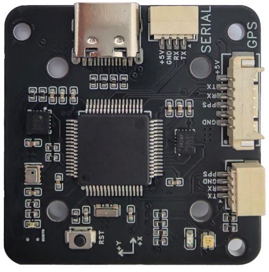
Introduction to QFN Packaging
What is QFN?
The Quad Flat No-lead (QFN) is a type of surface-mount package for electronic components. Unlike traditional packages that have pins protruding from the sides, QFN has a flat, leadless design, where the connections to the PCB (printed circuit board) are made through small pads on the bottom of the package. This makes it much smaller and more efficient compared to packages with leads, such as the QFP.
Evolution of QFN in the Electronics Industry
QFN packaging has grown in popularity over the years, particularly in high-performance sectors. Initially, traditional packaging solutions like Ball Grid Array (BGA) and Leadless Chip Carrier (LCC) were preferred due to their reliability and heat dissipation capabilities. However, these solutions were often bulky and more expensive.
As electronics became smaller and more power-demanding, manufacturers needed a solution that could support compact designs without sacrificing performance. The QFN package emerged as an effective solution, offering several advantages over older packaging types. For example, while QFP (Quad Flat Package) packages could be large and had high-profile leads, QFNs had no protruding pins, making them much more space-efficient.
In the 2000s, as industries like automotive and IoT grew, QFN quickly gained traction. Automotive systems, especially those in Advanced Driver Assistance Systems (ADAS), required a compact, reliable, and heat-efficient package to handle sensors and processing units. Similarly, IoT devices, with their need for smaller components and efficient energy use, turned to QFN to ensure long-lasting performance in devices like smartwatches, fitness trackers, and smart thermostats.
Today, QFNs are widely used in a range of high-performance applications, from medical devices (like portable glucose monitors and hearing aids) to consumer electronics and wireless communication systems. As the demand for smaller, more efficient devices continues to grow, QFN packaging is likely to remain a key technology in the electronics industry, shaping the future of everything from smart home devices to autonomous vehicles.
By continuously evolving to meet the needs of new industries, QFN packaging has cemented its place as a reliable, high-performance solution in modern electronics. Whether in wearables, automotive control systems, or Internet of Things (IoT) devices, the QFN package continues to thrive due to its unique combination of small size, high-frequency performance, and cost-effectiveness.
Key Features of QFN Packaging
Leadless Design
One of the standout features of the QFN package is its leadless design. Unlike traditional component packages, such as the QFP or BGA, QFN has no external leads. Instead, the electrical connections are made through pads on the bottom of the package. This design makes QFN components smaller and more compact, saving valuable space on the PCB (printed circuit board).
Comparison with traditional leaded packages: In a QFP, for example, the leads stick out from the sides, which increases the overall size of the package. On the other hand, the QFN’s leadless design reduces its footprint by about 25% compared to traditional leaded packages like QFP. This makes QFN especially beneficial in applications where space is limited, such as wearable devices, smartphones, or automotive electronics. Additionally, the flat profile of QFN allows for easier surface-mount assembly on the PCB, compared to the more complex assembly needed for traditional leaded packages.
Thermal Management
Thermal management is a critical consideration in electronics, especially for high-performance devices. QFN packages excel in this area due to their central thermal pad. This large thermal pad at the bottom of the package provides a direct path for heat to dissipate into the PCB. This is a huge advantage when compared to traditional packages like QFP, which may not have a dedicated thermal pad and require more complex heat management solutions.
The thermal resistance of a QFN package is typically between 20–30°C/W, meaning it can transfer heat more efficiently than many other package types. This makes QFN particularly useful for power-hungry applications, such as power ICs and high-speed processors. In real-world terms, this efficient heat dissipation helps prevent overheating, ensuring the longevity and reliable operation of devices in high-power or high-performance environments. For instance, automotive systems that rely on constant, high-speed data processing can benefit greatly from QFN’s superior thermal handling capabilities.
Electrical Performance
QFN packages are known for their excellent electrical performance, particularly in high-frequency applications. One of the main reasons for this is the shortened pad connections in QFN packages. With the pads located directly on the bottom of the package, the electrical paths are much shorter compared to packages like BGA, which often have through-hole connections. This results in minimized signal loss and faster signal transmission, making QFNs ideal for IoT devices, wireless communication modules (like Wi-Fi and Bluetooth), and other high-speed electronics.
In real-world applications, this advantage is crucial. For example, in a Bluetooth module, signal integrity is vital to ensure stable, fast connections. The shorter connections in QFN reduce the chances of signal degradation, which could lead to poor communication performance. As the world increasingly moves toward 5G technology and IoT, the demand for such high-frequency, low-loss performance makes QFN a preferred choice for many electronic designers.
Cost-Effectiveness
When it comes to cost-effectiveness, QFN packages offer a significant advantage over other package types like BGA and LCC . The production cost of plastic QFNs is considerably lower than that of other advanced packaging options. For example, plastic QFNs can cost between $0.10–$0.50 per component, whereas BGAs can cost $0.50–$2.00 per component. This price difference makes QFN a more affordable option for high-volume production.
QFN's simple design also means that it can be easily assembled using standard surface-mount technology (SMT). No special assembly techniques or equipment are required, which further lowers manufacturing costs. This makes QFN especially attractive to manufacturers of IoT devices or consumer electronics that require mass production at an affordable price point. For example, in the smart thermostat industry, where millions of units are produced, using QFN packaging allows manufacturers to keep production costs down while maintaining high performance.
Advantages of QFN Technology
Compact Form Factor
One of the key advantages of QFN technology is its compact form factor, making it ideal for small, space-constrained devices. The leadless design eliminates the need for protruding pins, which reduces the overall size of the component. This is especially beneficial for wearables like smartwatches, fitness trackers, and other devices that require small, lightweight components to fit in limited space. The small footprint allows manufacturers to design thinner and lighter devices without compromising performance.
Comparison with other packages: When compared to traditional packages like QFP and BGA, QFN packages offer a more compact solution. A QFP package has leads that extend outward from the sides, increasing the space needed on the PCB. In contrast, a QFN’s flat, leadless design saves about 25% of the space compared to a QFP of the same size. BGAs, while efficient, are typically larger and more complex to assemble, making QFN a more practical option for mass-market consumer electronics where space and cost are key factors.
Enhanced Heat Dissipation
QFN packages are designed with enhanced heat dissipation capabilities, which is critical for ensuring that high-performance components do not overheat during operation. The central thermal pad on the bottom of the QFN package provides a direct path for heat to move from the component into the PCB, where it can be spread and dissipated more efficiently. This design helps in maintaining the optimal operating temperature for the component, reducing the risk of overheating and performance degradation.
In power management applications, such as power ICs (Integrated Circuits) used in automotive systems, consumer electronics, and industrial devices, efficient heat dissipation is especially important. High-power devices generate significant heat, and QFN’s thermal pad helps prevent thermal buildup, allowing these devices to maintain stable performance. For example, a power supply unit in a smart thermostat can benefit from QFN's superior heat transfer, ensuring reliable long-term operation without the need for additional heat sinks or cooling systems.
Low-Cost Production
QFN technology is cost-effective, making it an attractive choice for manufacturers aiming to reduce overall production costs. The design of QFN packages is simpler compared to other advanced packaging solutions like BGA or LCC. This simplicity translates into lower manufacturing costs, especially in high-volume production. Plastic QFNs, which are widely used in mass production, are much cheaper to produce than more complex packages that require specialized assembly techniques.
In real-world terms, the cost savings can be significant. For example, plastic QFNs typically cost between $0.10 and $0.50 per unit, while BGA packages may cost between $0.50 and $2.00 per unit. This price difference makes QFNs a preferred choice for IoT devices, automotive electronics, and consumer gadgets that need to be affordable for mass-market adoption. In automotive applications, where millions of units may be required, the reduced cost of QFN packages allows manufacturers to offer high-quality, reliable products at a competitive price point.
Ease of Assembly
Another significant advantage of QFN technology is its ease of assembly. QFN packages are fully compatible with SMT, which is the standard method for assembling electronic components onto a PCB. SMT is widely used because it is fast, efficient, and cost-effective. QFN packages can be easily mounted on the PCB using standard SMT equipment, without requiring special assembly tools or techniques.
Comparison to other packages: Unlike other advanced packages such as BGA, which often require specialized equipment for placing and soldering the component, QFN’s simplicity allows it to be easily incorporated into existing manufacturing processes. This makes it an attractive choice for high-volume production, where minimizing assembly complexity and costs is crucial. For example, manufacturers of consumer electronics like smartphones or smart home devices benefit from QFN's ability to be seamlessly integrated into existing SMT production lines, speeding up the manufacturing process and reducing labor costs.
Applications of QFN Packaging
Automotive
QFN packaging is widely used in the automotive industry due to its ability to withstand harsh environments and deliver high-performance results. It is commonly found in electronic control units (ECUs), which manage various vehicle systems such as fuel injection, anti-lock braking systems (ABS), and ADAS. These systems require reliable and durable components to function in demanding conditions, such as extreme temperatures and vibrations.
The reliability of QFN packaging in these environments comes from its efficient heat dissipation and compact design. Automotive components often operate in a wide temperature range (from -40°C to 150°C), making thermal management crucial. QFN’s thermal pad provides a direct path for heat to dissipate, helping to ensure stable performance and preventing overheating in critical systems. For example, in ADAS sensors, which help with features like lane-keeping and collision avoidance, maintaining precise function in fluctuating temperatures is vital for driver safety.
IoT & Wearables
The IoT and wearable devices often require components that are both small in size and high in performance. QFN packages are ideal for this purpose, providing a compact form factor that fits into devices like smartwatches, fitness trackers, and wireless modules (such as Bluetooth). These devices need reliable connectivity and efficient power management, both of which QFN technology excels at.
For IoT devices, space is always a concern. Many IoT products must fit into small enclosures, and the compact design of QFN helps save precious space on the circuit board. The leadless design and the use of shortened pad connections contribute to a more efficient layout, enabling smaller, lighter devices with minimal compromise on performance. For example, in a smartwatch processor, where every millimeter counts, QFN’s small size and heat dissipation capabilities ensure both compactness and performance.
Medical Devices
QFN packaging is also gaining popularity in the medical device sector, where size, reliability, and low power consumption are crucial. For portable devices like glucose monitors and hearing aids, QFN's small size makes it an ideal choice. These devices are often worn or carried by the user, requiring components that can be as small as possible without sacrificing performance.
The low power consumption of QFN packages is particularly beneficial in health monitoring devices. Since many medical devices rely on battery power, minimizing power usage helps extend battery life. For example, a glucose monitor using QFN packaging can function for long periods without frequent recharging, improving convenience for the user. The reliability and efficiency of QFN packaging also help ensure the devices remain accurate and stable over time, which is essential for health applications.
Home Electronics
QFN packaging is commonly used in various home electronics like smart thermostats, LED drivers, and Wi-Fi routers. These devices often require compact components that still deliver reliable connectivity and performance. QFN’s space-saving design and thermal management capabilities make it a perfect choice for consumer electronics that need to operate efficiently in compact enclosures.
For instance, in Wi-Fi routers, QFN’s short pad connections help improve signal integrity and minimize signal loss, ensuring fast, stable connections. The small form factor also enables manufacturers to fit multiple features into a single device without increasing its size. In smart thermostats, the use of QFN packages allows for low-cost production while still maintaining the performance needed to regulate home temperatures accurately. The compact design also helps make the devices more aesthetically pleasing and easier to install in homes.

Potential Challenges with QFN Packaging
Solder Joint Inspection
One of the most significant challenges in using QFN packaging is the hidden solder joints. Unlike traditional packages, where the pins are visible from the sides, the solder joints in QFN packages are located on the bottom of the component, particularly on the large thermal pad. This makes inspecting the quality of the solder joints more difficult since they are not visible during standard inspection methods.
X-ray inspection is often required to detect issues such as solder voids or cold solder joints—problems that can impact the electrical and thermal performance of the device. Without proper inspection, solder defects could lead to intermittent connections, overheating, or device failure.
To address this challenge, manufacturers can use specialized X-ray inspection equipment that allows them to look inside the package and examine the solder joints on the thermal pad. This ensures the joints are properly formed and free of defects. Other tools, like automated optical inspection (AOI) and high-precision soldering machines, can also be employed to improve the reliability of the soldering process. By using these tools, manufacturers can detect potential issues early, ensuring high-quality production and reducing the risk of component failure.
Placement Accuracy
Another challenge with QFN packaging is ensuring precise placement during the assembly process. Because the solder pads on the bottom of the package are very small and closely spaced, even a slight misalignment (as small as 0.1mm) can lead to placement errors. These errors can cause the pads to misalign with the traces on the PCB, resulting in poor connections, short circuits, or open circuits.
Misplacement issues can have serious consequences for device performance. For example, a misaligned QFN could lead to pad-to-trace shorts, where the solder connects unintended parts of the PCB, potentially causing signal interference or power issues. Even small defects can affect the overall electrical performance, especially in high-frequency applications like IoT devices or wireless modules, where precision is crucial.
To avoid these problems, placement accuracy is critical. Manufacturers often use pick-and-place machines with high precision and advanced optical alignment systems to ensure the QFN package is correctly positioned on the PCB. These systems can help reduce the risk of misplacement, ensuring the package’s pads align perfectly with the PCB’s traces. Additionally, engineers may design land patterns on the PCB that help guide the QFN into the correct position, further improving the assembly process.
Pin Count Limitations
QFN packages are generally designed with 12 to 64 pins, making them suitable for applications that don’t require a large number of connections. However, this limited pin count becomes a limitation when designing complex systems that require a higher number of connections—for example, high-performance System on Chips (SoCs) or processors with hundreds of I/O pins.
QFN’s design is not ideal for such high-pin-count devices because it can quickly become difficult to manage the increased number of pads on the bottom of the package. As the pin count increases, the thermal pad may also become smaller, reducing the package’s ability to efficiently dissipate heat. Furthermore, the more pins a device has, the more complex the layout becomes, which may lead to signal integrity issues or increased manufacturing complexity.
For complex SoCs or high-functioning processors that require hundreds of pins for data transfer and power distribution, packages like BGA are often preferred. BGAs offer a greater number of connections and more flexible layout options, making them suitable for advanced processors and high-performance systems. In contrast, QFN’s smaller pin count is ideal for low to mid-complexity devices where space and cost are a priority, but it’s less effective in handling the requirements of extremely complex systems.
Design Considerations for QFN Packages
PCB Layout for QFN
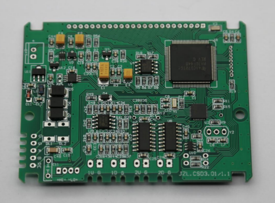
When designing a PCB for QFN packages, it is important to follow best practices to ensure optimal performance and reliability. The most crucial design factors include pad size, spacing, and thermal considerations. These elements are vital for proper soldering, heat dissipation, and electrical performance.
1. Pad Size and Spacing:
For QFN packages, the pad size must match the dimensions of the solder pads on the bottom of the package. Too small or too large a pad can lead to poor solder joints and reduce the connection reliability. Proper spacing between the pads is also necessary to prevent short circuits. Generally, the spacing should follow industry standards to ensure proper electrical conductivity.
2. Thermal Considerations:
Since QFN packages often handle high-performance components that generate heat, it is essential to include thermal pads in the PCB layout. These pads are crucial for dissipating heat efficiently. The thermal pad should have enough copper area to transfer heat effectively to the PCB. Additionally, vias (small holes) should be used around the thermal pad to conduct heat into the inner layers of the PCB, enhancing thermal dissipation. This is especially important in power ICs and high-speed applications where heat management is critical.
By following these guidelines, the QFN package can be integrated into the PCB with maximum performance and minimal risk of failures due to poor heat management or electrical issues.
Soldering and Assembly Process
The soldering and assembly process for QFN packages follows the standard SMT process. However, due to the leadless design and bottom-side pads, special care is required to ensure reliable soldering.
Step 1 - Solder Paste Application:
The first step in the assembly process is applying solder paste to the PCB pads where the QFN will be placed. The paste is a mixture of tiny solder balls and flux, applied using a stencil. It is important to apply the paste evenly to ensure a strong bond between the QFN and the PCB.
Step 2 - Component Placement:
After the paste is applied, the QFN component is placed on the PCB. Pick-and-place machines are used to position the QFN package precisely onto the solder pads. Because the pads on QFNs are on the bottom, precise placement is essential to avoid misalignment.
Step 3 - Reflow Soldering:
Once the component is in place, the PCB goes through a reflow oven, where the temperature is gradually increased to melt the solder paste. This process forms solid solder joints between the QFN and the PCB. The temperature profile in the reflow oven is critical to ensure that the solder melts and then cools in a controlled way, forming strong, reliable connections.
Step 4 - Post-Reflow Inspection:
After the reflow process, the solder joints must be inspected. For QFN packages, this often involves X-ray inspection due to the hidden solder joints on the thermal pad. This helps verify that the solder joints are free from defects, such as cold solder joints or solder voids, which can lead to poor performance or failure.
By following these steps carefully, manufacturers can ensure that the QFN package is securely and correctly soldered onto the PCB.
Quality Control and Testing
Once the soldering and assembly processes are complete, it is crucial to perform thorough quality control and testing to ensure that the QFN package is functioning as intended. This includes checking the solder joints, heat dissipation performance, and electrical functionality.
1. Solder Joint Verification:
Since QFN packages have hidden solder joints on the bottom, X-ray inspection is often used to check for solder voids or misaligned joints. X-ray machines can scan through the package and show detailed images of the solder joints, allowing manufacturers to detect issues that could cause poor electrical connections or overheating.
2. Heat Dissipation Testing:
Heat dissipation is another critical factor in ensuring the QFN package works properly. Testing involves checking that the thermal pad is effectively transferring heat from the component into the PCB. This can be done by monitoring the temperature of the component under load and ensuring it stays within safe operating limits. If the thermal performance is inadequate, the device may overheat and fail prematurely.
3. Electrical Functionality Testing:
Finally, electrical testing is essential to verify that the QFN package is properly connected and functional. This includes checking for continuity between the pads and traces, as well as ensuring that the component works correctly within the circuit. Specialized testing equipment, such as automated electrical testers or oscilloscopes, can be used to check the component’s electrical performance.
By implementing these quality control measures and using advanced testing tools like X-ray inspection, manufacturers can ensure that the QFN package performs reliably in its application, reducing the risk of defects and improving overall product quality.
Comparing QFN with Other Common Package Types
QFN vs. QFP
QFN and QFP are both surface-mount packages used in electronic devices. However, they differ in terms of size, cost, and performance.
Size:
The key difference between QFN and QFP is the size. QFNs have a leadless design with pads on the bottom of the package, allowing for a smaller overall footprint. In comparison, QFP packages have leads that extend outward, making them larger and requiring more space on the PCB. For instance, a QFN with 32 pins might only occupy a 5mm × 5mm area, whereas a QFP with the same pin count could take up a 7mm x 7mm area. This makes QFN ideal for space-constrained applications like wearables and smartphones.
Cost:
QFN packages are generally cheaper than QFP packages. This is because QFN's leadless design is simpler to manufacture, and the assembly process typically requires fewer steps. On average, QFNs can cost between $0.10–$0.50 per unit, while QFPs tend to be more expensive, often ranging from $0.50–$2.00 per unit. This price difference makes QFN more suitable for high-volume production in consumer electronics and IoT devices.
Performance:
QFNs offer superior thermal management compared to QFPs. The large thermal pad on the bottom of a QFN facilitates better heat dissipation, which is crucial for power-hungry applications. In contrast, QFPs typically require additional components like heat sinks or external thermal management solutions. This makes QFN the better choice for high-power or high-frequency applications where heat management is a priority.
In summary, QFN packages are smaller, cheaper, and have better thermal management than QFPs, making them ideal for compact, cost-sensitive, and high-performance devices.
QFN vs. BGA
QFN and BGA are both used for high-performance devices, but they have different strengths and trade-offs.
Heat Dissipation:
While both QFN and BGA have thermal pads for heat dissipation, BGAs typically offer better thermal performance due to their larger number of connections and more efficient heat spread through the entire package. This makes BGA a better choice for high-power applications like processors in computers or advanced automotive systems. However, QFN packages are still competitive in many situations, especially for medium-power devices, as their thermal pads are also highly effective at directly transferring heat to the PCB.
Cost:
QFN packages are generally more cost-effective than BGA packages. QFN uses a simpler manufacturing process with fewer steps, resulting in lower production costs. BGAs, on the other hand, are more complex and require more precise manufacturing, especially when dealing with the ball grid. This complexity leads to a higher cost, which can be a disadvantage when working on budget-sensitive projects or mass production.
Performance:
Both QFN and BGA provide low signal loss and high-frequency performance, making them suitable for IoT devices, wireless modules, and consumer electronics. However, BGA is typically chosen for high-pin-count devices (such as CPUs or high-end SoCs), where a larger number of connections is needed. QFN, with its limited pin count (typically 12–64 pins), is better suited for mid-complexity applications.
In conclusion, QFN is more cost-effective and suitable for lower-pin-count, medium-power devices, while BGA offers better heat dissipation and higher performance for high-pin-count, high-power applications.
QFN vs. LCC
QFN and LCC are both leadless packages, but they differ in electrical performance, cost, and applications.
Electrical Performance:
QFN packages generally offer better electrical performance than LCC. The pad layout in QFN packages ensures shorter electrical paths, which minimizes signal loss and improves high-frequency performance. This makes QFN a better choice for applications such as Bluetooth modules, Wi-Fi chips, and RF circuits. LCCs, on the other hand, may not provide the same level of performance, especially in high-speed applications, due to longer connections.
Cost:
In terms of cost, both QFN and LCC are generally affordable, but QFN packages tend to be slightly cheaper due to the simpler manufacturing process. LCC packages are often used in specialized applications, which may involve higher costs due to their more complex designs and specific manufacturing requirements. For mass production of low- to medium-pin-count devices, QFN packages provide a more economical solution.
Applications:
LCC packages are often used for low-pin-count applications, such as power ICs or simple sensors, where performance requirements are less demanding. QFN, on the other hand, is more suitable for applications requiring high-frequency operation and thermal management, such as in IoT devices, smartphones, and wearable technology.
In summary, QFN provides better electrical performance and is more cost-effective than LCC, making it ideal for high-frequency applications in consumer electronics, while LCC can still be used for simple, low-pin-count applications with less emphasis on performance.
Comparison Table
Feature QFN QFP BGA LCC Size Smaller, compact design Larger, with external leads Larger, with more pins and balls Compact, but typically larger than QFN Cost Low cost Higher cost Higher cost Moderate cost Thermal Management Excellent, with large thermal pad Requires external solutions Best heat dissipation Good, but not as efficient as QFN Performance High-frequency, low-loss Good for mid-complexity High-performance, high-pin-count Lower performance, suited for simple circuits Pin Count 12–64 pins 20–200+ pins Hundreds of pins 4–40 pins Best Use Power ICs, IoT devices, wearables Consumer electronics, automotive High-performance processors Low-pin-count sensors, simple ICs
Conclusion
Choosing the right package for your components is crucial for optimal performance and cost-efficiency. QFN packages excel in compactness, thermal management, and cost-effectiveness, making them ideal for a wide range of applications.
For businesses seeking high-quality PCBs, PCBMASTER, a trusted and experienced PCB supplier, offers tailored solutions for QFN and other packaging types. With precision and reliability, PCBMASTER ensures your designs meet the highest standards of performance and quality.
FAQs
Why is QFN often used in automotive electronics?
QFN packages are ideal for automotive electronics due to their robustness and superior heat dissipation. Automotive systems require components that can withstand harsh environments, including extreme temperatures ranging from -40°C to 150°C. The large thermal pad on the bottom of QFN packages efficiently transfers heat to the PCB, making them perfect for power ICs and sensors used in systems like ECUs, ABS, and ADAS. This ensures that automotive electronics maintain reliability and performance even under demanding conditions.
Can QFN be used for high-pin-count ICs?
While QFN packages are excellent for applications with low to medium pin counts, they are unsuitable for complex systems requiring more than 64 pins. This is because QFN packages typically support between 12 to 64 pins, which limits their ability to handle high-pin-count ICs such as complex SoCs or multi-core processors. For devices that need hundreds of pins, packages like BGA are preferred, as they provide better pin density and electrical performance.
What is the key advantage of QFN's leadless design?
The most significant advantage of QFN's leadless design is its compact size and space savings. Unlike traditional packages like QFP, QFN packages have no leads protruding from the sides, reducing the overall footprint by up to 25%. This makes QFN an excellent choice for space-constrained applications, such as wearables, smartphones, and IoT devices, where minimizing the size of the PCB is critical without compromising performance or functionality.
How do manufacturers inspect QFN solder joints?
Inspecting QFN solder joints is more challenging than traditional packages because the solder pads are located on the bottom of the package, especially the large thermal pad. X-ray inspection is typically used to check for hidden solder joints and detect issues like solder voids or cold solder joints, which could lead to poor electrical connections or overheating. This non-destructive method allows manufacturers to ensure the integrity of the solder joints, which is crucial for the long-term reliability of the component.
What are the cost advantages of QFN compared to other packaging types?
QFN packages offer significant cost savings over other packaging types like BGA or QFP. The simpler manufacturing process of QFNs, combined with their leadless design, makes them more affordable to produce, especially in high-volume manufacturing. While BGA packages are often more expensive due to their complexity and higher pin count, QFN packages can cost as little as $0.10–$0.50 per unit, compared to $0.50–$2.00 for QFPs or BGAs. This cost advantage makes QFN a popular choice for consumer electronics, IoT devices, and other cost-sensitive applications.
Author Bio
Hi, I'm Carol, the Overseas Marketing Manager at PCBMASTER, where I focus on expanding international markets and researching PCB and PCBA solutions. Since 2020, I've been deeply involved in helping our company collaborate with global clients, addressing their technical and production needs in the PCB and PCBA sectors. Over these years, I've gained extensive experience and developed a deeper understanding of industry trends, challenges, and technological innovations.
Outside of work, I'm passionate about writing and enjoy sharing industry insights, market developments, and practical tips through my blog. I hope my posts can help you better understand the PCB and PCBA industries and maybe even offer some valuable takeaways. Of course, if you have any thoughts or questions, feel free to leave a comment below—I'd love to hear from you and discuss further!


