


What Is a PCB Printed Circuit Board? A Complete Guide to PCB Design
Beneath the sleek surfaces of modern electronics lies a hidden structure that makes everything possible: the printed circuit board (PCB). It’s a piece of technology that, while often overlooked, is integral to the functionality of devices we rely on daily. From the precision required in its design to the advanced materials used in its creation, the process of crafting a PCB is a delicate balance of engineering, innovation, and detail. But what exactly goes into creating these vital components, and why do they matter so much in the tech we use? Let’s unravel the world of PCBs and discover how they play a critical role in shaping the future of electronics.
Introduction to PCB Printed Circuit Boards
What is a PCB?
A printed circuit board (PCB) is a flat, rigid board used to mechanically support and electrically connect electronic components using conductive pathways, or traces. PCBs are typically made of an insulating material, like fiberglass, and are layered with copper to form the circuits. These boards are crucial for ensuring that components like resistors, capacitors, and microchips work together within a device.
PCBs serve as the backbone of nearly all electronic devices, from simple gadgets like calculators to complex systems such as smartphones, computers, and medical equipment. Without PCBs, the complex networks of electrical connections that make these devices function wouldn’t exist.
Purpose of a PCB in Electronic Devices
PCBs provide a stable, organized platform for components to be securely attached while ensuring proper electrical connections. They serve three key functions:
Mechanical Support: PCBs hold electronic components in place, providing structure and stability.
Electrical Pathways: The copper traces on PCBs allow electrical signals to flow between components.
Heat Dissipation: PCBs help to distribute heat produced by components, preventing overheating.
Brief History and Evolution of PCBs
The first PCBs were introduced in the 1930s, but it wasn’t until the 1950s that they became widely used in consumer electronics. Initially, PCBs were simple and used for basic wiring and connections. However, as electronic devices became more complex, so did PCBs. Today, we have multi-layer PCBs capable of supporting high-performance components in everything from wearables to spacecraft. Over the decades, advancements in PCB manufacturing techniques, like surface-mount technology (SMT), have allowed for more compact, efficient, and powerful devices.
Importance of PCBs in Modern Electronics
PCBs play a vital role in nearly every modern electronic device. Their influence can be seen in several key areas:
1. Miniaturization of Electronics
As consumer demand grows for smaller, more powerful devices, the importance of PCBs in achieving miniaturization cannot be overstated. Multi-layer PCBs, for example, allow for the stacking of electrical connections, which reduces the space needed for circuits while maintaining functionality. This has enabled the development of compact, portable devices like smartphones, laptops, and wearables.
2. Ensuring Reliability and Functionality
In critical systems like automotive electronics, medical devices, and aerospace technology, PCBs are designed to ensure high reliability and long-term functionality. In automotive systems, for example, PCBs are used in everything from engine control units (ECUs) to infotainment systems. In medical devices, PCBs ensure that diagnostic tools, like ECG machines and pacemakers, operate safely and accurately. Their reliability directly impacts the performance of these devices, making quality PCB design essential.
3. Cost-Effectiveness and Versatility
PCBs enable cost-effective mass production of electronic devices while maintaining high standards of performance. With the ability to incorporate multiple components on a single board, PCBs reduce the need for bulky wiring and minimize assembly time, lowering manufacturing costs.
Basic Types of PCBs
PCBs come in various forms, each designed to meet the specific needs of different devices. Here’s a breakdown of the three most common types of PCBs:
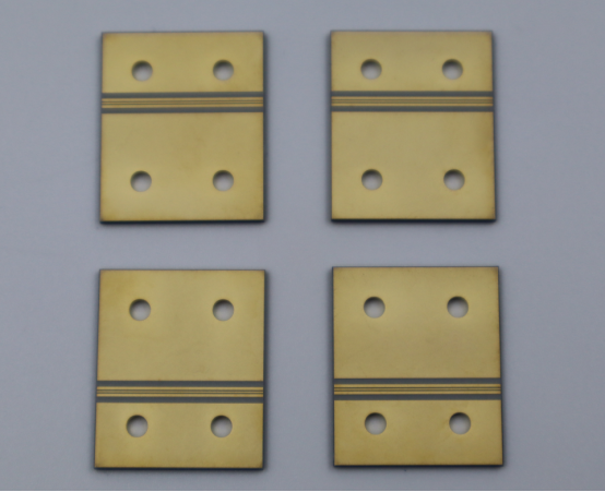
Single-Sided PCBs: Simple, Low-Cost Applications
Single-sided PCBs are the most basic type, where all the electronic components are placed on one side of the board. The copper traces are etched onto the opposite side. These PCBs are commonly used in low-cost consumer electronics, such as calculators, light fixtures, and basic home appliances. They are straightforward to design and manufacture, making them cost-effective for mass production.
Example: Many simple electronic toys and household items use single-sided PCBs because they are inexpensive to produce.
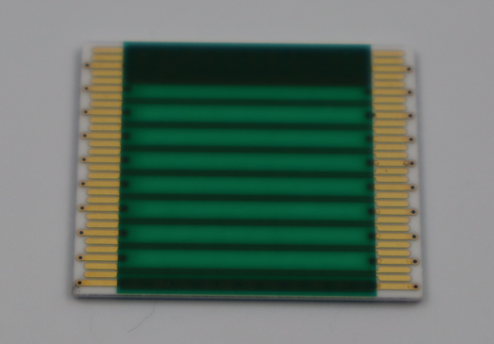
Double-Sided PCBs: Used in More Complex Devices
Double-sided PCBs have copper traces on both sides of the board, allowing for more complex designs and greater functionality. These PCBs can accommodate more components, and their two-sided layout enables more efficient use of space. Double-sided PCBs are often used in audio devices, power supplies, and communication equipment, where more components need to be connected but space is still limited.
Example: A power adapter for an electronic device might use a double-sided PCB to handle the higher number of connections and components involved in converting voltage.
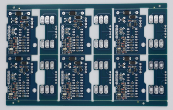
Multi-Layer PCBs: For High-Performance Devices Like Smartphones and Computers
Multi-layer PCBs consist of several layers of copper and insulating materials stacked together, allowing for a much higher density of components and complex circuit routing. These PCBs are essential for high-performance applications, such as smartphones, computers, and high-frequency communication systems. The layers are carefully designed to ensure signal integrity and prevent interference between components.
Example: The PCB inside a smartphone features multiple layers to accommodate various components like processors, memory chips, and antennas, while keeping the device thin and lightweight.
Each type of PCB offers distinct advantages, depending on the complexity of the device and the performance requirements. Whether it’s a simple home appliance or a high-tech smartphone, PCBs are the foundation that allows modern electronics to function as seamlessly as they do.
The Components and Materials of a PCB
Key Components of a PCB
A printed circuit board (PCB) consists of several essential components, each playing a crucial role in its functionality and performance. Here’s a breakdown of the key parts:
Substrate: The Foundation of the PCB
The substrate is the base layer of the PCB, providing the structural support needed for the entire board. Typically made from materials like fiberglass or epoxy resin, the substrate is lightweight, durable, and resistant to heat. Its primary function is to serve as a rigid foundation on which other layers, such as copper traces and solder masks, are applied.
Example: The FR4 material, a composite of fiberglass and epoxy resin, is the most widely used substrate in PCB manufacturing due to its excellent balance of cost, strength, and insulating properties.
Conductive Layers: Copper Layers for Electrical Connections
The conductive layers are made of copper and form the electrical pathways that connect various components on the PCB. These layers are etched to create copper traces, which act as the "wires" of the circuit, allowing electricity to flow between different components. The thickness and layout of these traces are carefully designed to handle the required electrical load and ensure signal integrity.
Example: In a multi-layer PCB, copper traces are sandwiched between layers of insulating material, enabling more complex and compact circuit designs.
Solder Mask: Preventing Short Circuits
The solder mask is a thin layer of protective coating applied over the copper traces. Its primary function is to prevent short circuits by insulating the copper traces from accidental contact with other conductive materials. The solder mask also protects the PCB from environmental damage, such as moisture, dust, and oxidation, which can degrade performance over time.
Example: The green color commonly seen on PCBs is the solder mask, though it can also come in red, blue, and black depending on the manufacturer’s choice.
Silkscreen: Labels and Markings for Component Placement
The silkscreen layer is used for labeling and marking important information on the PCB, such as component placements, logos, and identification numbers. This layer is essential for assembly, as it guides manufacturers in placing components accurately on the board. The silkscreen is usually applied using an ink printing process and is typically white or yellow in color.
Example: On a PCB, you’ll often find labels like “R1” for resistors or “C2” for capacitors, which are placed on the silkscreen layer to ensure correct component placement.
Materials Used in PCB Manufacturing
The choice of materials in PCB manufacturing plays a significant role in determining the board’s performance, cost, and application suitability. Here are the most commonly used materials:
FR4: The Most Common PCB Material
FR4 is the standard material used in most PCBs due to its combination of cost-effectiveness, mechanical strength, and insulating properties. It is a fiberglass-reinforced epoxy resin that offers durability and resistance to heat, moisture, and chemicals, making it ideal for general-purpose applications.
Example: Consumer electronics, such as smartphones and laptops, typically use FR4 PCBs due to their versatility and reliable performance at an affordable cost.
CEM1 and CEM3: Alternative Materials for Specific Applications
CEM1 and CEM3 are alternative materials used for specific types of PCBs. These materials are made from a composite of fiberglass and paper or epoxy resin, offering similar insulating properties to FR4 but at a lower cost. They are often used in single-sided or low-cost PCBs where high-performance characteristics are not critical.
CEM1: Made with a paper core and a layer of epoxy resin, often used in low-frequency or basic consumer electronics.
CEM3: Similar to CEM1, but with better mechanical properties and a higher temperature resistance, often used in consumer devices like calculators or household electronics.
High-Frequency Materials: For High-Performance or RF Devices
For applications requiring high-frequency signals, such as radio-frequency (RF) devices or 5G communication systems, specialized materials are used to minimize signal loss and distortion. These materials, such as PTFE (Teflon) and ceramic-filled resins, have superior dielectric properties that help maintain signal integrity at high frequencies.
Example: High-frequency PCBs are used in mobile phones, GPS systems, and wireless communication devices, where fast and reliable signal transmission is crucial.
The components and materials used in PCB design and manufacturing determine the overall performance, durability, and functionality of the circuit board. Understanding these foundational elements is key to creating high-quality, reliable PCBs that meet the demands of modern electronics. By selecting the right materials and ensuring precise fabrication, engineers can design PCBs that support everything from simple devices to cutting-edge technologies.
PCB Design Process
The Basics of PCB Design
Designing a printed circuit board (PCB) is a multi-step process that transforms an electronic circuit concept into a physical, functional board. The design process involves several critical stages, each building on the previous one. Here’s a closer look at the basic steps involved in PCB design:
Schematic Design: Creating a Blueprint for the Circuit
The first step in PCB design is creating the schematic, which acts as a blueprint for the entire circuit. This schematic shows how all the components (resistors, capacitors, ICs, etc.) are connected and how electrical signals flow between them. It is essential to ensure that all connections are correct before moving to the next stage.
Example: In the schematic, a microcontroller might be connected to a set of sensors, with each sensor's specific pinout shown to indicate how it should be wired on the PCB.
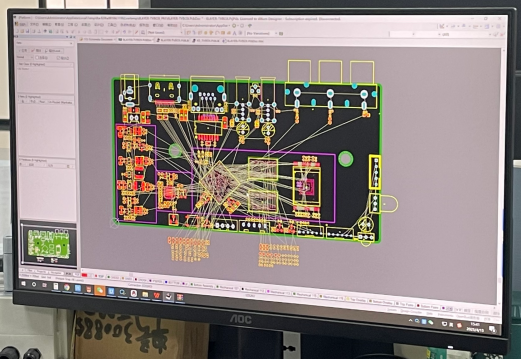
Layout Design: Arranging Components on the PCB
Once the schematic is complete, the next step is to move to layout design, where you arrange the physical components on the PCB. This step involves choosing the locations for each component on the board while considering factors like size, space constraints, and component orientation. Good layout design ensures that the PCB functions properly and fits within the device’s form factor.
Example: The layout might include placing a microprocessor at the center of the board, with its associated capacitors and resistors nearby to minimize trace lengths and improve performance.
Trace Routing: Designing Electrical Paths Between Components
After the components are placed, the next task is trace routing, which involves designing the copper paths that will connect the components. These traces carry electrical signals and power across the board. Trace routing requires careful planning to avoid interference, ensure signal integrity, and prevent short circuits.
Example: For high-frequency applications, traces might need to be kept as short and straight as possible to reduce signal loss. In contrast, low-frequency designs can have longer traces but must still maintain proper spacing.
PCB Design Tools and Software
The design process today is heavily aided by specialized PCB design software, which makes it easier to create complex layouts, check for errors, and optimize the design for manufacturability. Here are the most commonly used tools:
Common Software Tools: Altium Designer, Eagle, KiCad, etc.
There are several software tools available for PCB design, each with unique features and capabilities. Some of the most popular include:
Altium Designer: A high-end tool used by professionals for complex designs, offering a wide range of features, including integrated schematic capture, layout, and simulation.
Eagle: A user-friendly, cost-effective tool often used by hobbyists and small businesses, with a strong community and extensive library of components.
KiCad: An open-source, feature-rich tool that is suitable for both beginners and professionals. It provides free access to advanced PCB design capabilities, including schematic capture and 3D visualization.
These tools help simplify tasks like creating component footprints, checking for electrical errors, and generating design files for manufacturing.
How Design Tools Aid in RAO: Automating Layout Optimization, Error Checking, and Generating Manufacturable Files
RAO (Retrieval-Augmented Optimization) can greatly benefit from PCB design tools by automating many aspects of the design process. For instance, software tools can optimize layout by automatically adjusting component placement and trace routing for better performance and lower manufacturing costs. They also perform error checking in real-time, highlighting issues like unconnected nets, short circuits, or design rule violations before the design is finalized.
Example: Altium Designer includes a built-in Design Rule Checker (DRC) that flags any violations of predefined design rules, such as incorrect trace widths or spacing, which helps avoid costly errors in the manufacturing process.
Designing for Manufacturability (DFM)
Designing a PCB isn’t just about creating a functional circuit—it’s also about ensuring that the design is easy and cost-effective to manufacture. Design for Manufacturability (DFM) involves considering various factors that will make the board easier and cheaper to produce, while still meeting performance requirements.
Design Rules: Guidelines for Clearances, Trace Widths, and Hole Sizes
One of the core principles of DFM is ensuring that the PCB adheres to design rules. These rules cover aspects like the minimum trace widths, clearances between traces, and hole sizes for components. If these rules are violated, it can lead to manufacturing issues, such as difficulty in soldering or the risk of short circuits.
Example: A typical rule might specify that traces carrying high current should have a minimum width to handle the power without overheating, while signal traces must be kept at a specific width to prevent signal degradation.
Layer Stack-up: Optimizing the Number of Layers for Cost and Performance
Layer stack-up refers to the arrangement of conductive and insulating layers in a multi-layer PCB. A well-optimized layer stack ensures the PCB meets electrical performance requirements without increasing costs unnecessarily. Using fewer layers reduces material costs, but too few layers can lead to signal interference or poor performance. The challenge lies in balancing cost-effectiveness with performance.
Example: For high-speed designs, additional layers might be used to separate power and ground planes from signal traces, helping to reduce noise and interference. On the other hand, a simple two-layer PCB may be enough for low-frequency devices.
Tolerance Levels: Ensuring Design Precision for High-Quality Fabrication
Tolerance levels refer to the acceptable variation in the manufacturing process, such as the dimensions of traces or holes. Designing within the manufacturer’s tolerances ensures that the final PCB is high-quality and functional. Tolerance levels must be carefully selected to match the capabilities of the PCB fabricator and the requirements of the application.
Example: A medical device PCB might require tighter tolerances to ensure the exact placement of components for sensitive signal processing, while a consumer product may be more forgiving of minor variations.
The PCB design process is a crucial part of creating reliable and high-performance electronic devices. By mastering the basics, using the right design tools, and considering manufacturability from the outset, designers can create PCBs that not only meet functional requirements but are also optimized for cost, efficiency, and ease of production. By following DFM principles and leveraging advanced design tools, engineers can help ensure their PCB designs are both effective and ready for real-world application.
Testing and Quality Assurance in PCB Manufacturing
PCB Testing Methods
Once a PCB is manufactured, it undergoes a series of tests to ensure its functionality, quality, and reliability. These tests help identify defects, prevent failures, and guarantee that the PCB performs as intended in its final application. Here are the primary testing methods used in PCB manufacturing:
Electrical Testing: In-Circuit Testing (ICT) vs. Functional Testing (CT)
Electrical testing is a crucial step in verifying that all components on a PCB are functioning properly and that there are no electrical faults, such as short circuits or open circuits. Two main types of electrical testing are commonly used:
In-Circuit Testing (ICT): ICT is used to test the individual components and interconnections on the PCB while it is in its final assembly form. Special test probes are placed on the PCB, and the board is powered up to check for electrical continuity and verify that all components are correctly connected and working within their specified parameters.
Example: ICT would be used to ensure that a resistor is properly connected to its respective trace, and a capacitor is functioning within its specified tolerance.
Functional Testing (FCT): FCT involves testing the entire PCB within the context of its intended application. It simulates how the PCB will operate in the final product by applying signals and verifying outputs. This type of testing ensures that the board works as part of the overall system and meets its functional specifications.
Example: In a PCB used for a power supply, FCT would test the entire circuit's ability to regulate voltage and current, simulating real-world electrical loads.
Visual Inspection: Ensuring the PCB is Free of Defects
Visual inspection is one of the simplest, yet highly effective, methods of PCB testing. During this process, the PCB is carefully examined by human inspectors or automated systems to identify any obvious defects or imperfections. These can include things like:
Misaligned components
Missing components
Soldering defects (cold joints, bridges, or insufficient solder)
Etching issues (incorrect or incomplete copper traces)
Example: Visual inspection might be used to check for any visible issues in the PCB’s surface mount technology (SMT) components, ensuring they are properly seated and soldered.
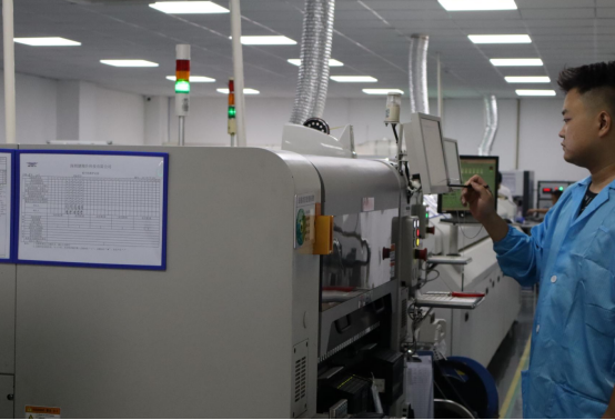
Automated Optical Inspection (AOI): Identifying Issues in the Production Line Through Machine Vision
Automated Optical Inspection (AOI) uses high-resolution cameras and machine vision software to automatically inspect a PCB for defects. AOI systems scan the board and compare the actual image of the PCB against the design files to identify discrepancies. This method is highly efficient, as it can quickly detect defects such as:
Misplaced components
Soldering issues
Missing or incorrect traces
Example: AOI systems can identify tiny solder bridges between adjacent pads, which could cause a short circuit. This inspection process is faster and more accurate than manual visual inspection, particularly in high-volume production runs.
Ensuring Quality Standards
Ensuring the quality of a PCB goes beyond just passing individual tests; it also involves adhering to industry standards and regulations that govern the design, materials, and manufacturing processes. By meeting these standards, PCB manufacturers can provide reliable products that meet customer expectations and regulatory requirements.
ISO Certification: The Importance of International Standards for PCB Manufacturers
ISO certification ensures that a PCB manufacturer follows internationally recognized quality management systems. The ISO 9001 standard, for example, outlines the requirements for a comprehensive quality management system and focuses on customer satisfaction, continuous improvement, and defect prevention. Certification indicates that the manufacturer adheres to best practices in production, documentation, and process control, resulting in higher-quality PCBs.
Example: A PCB manufacturer with ISO 9001 certification would be able to consistently produce PCBs that meet the exacting requirements of industries like aerospace, where quality and reliability are paramount.
RoHS Compliance: Environmental Impact and Lead-Free Soldering Requirements
RoHS (Restriction of Hazardous Substances) compliance is a critical quality assurance standard in PCB manufacturing. This regulation restricts the use of certain hazardous materials in electronic products, such as lead, mercury, cadmium, and other toxic substances. Lead-free soldering is a key component of RoHS compliance, as traditional solders containing lead can pose significant environmental and health risks.
Example: A PCB used in a consumer electronic device like a smartphone must be RoHS compliant, ensuring that all components and solder materials meet the lead-free standards, thus reducing the environmental impact of electronic waste.
Testing and quality assurance are integral to PCB manufacturing. By using a combination of electrical testing methods, visual inspections, and automated optical inspections, manufacturers can ensure that PCBs are free of defects and function as intended. Additionally, adhering to global standards like ISO certification and RoHS compliance ensures that PCBs meet not only performance expectations but also environmental and regulatory standards. This comprehensive approach to testing and quality control ultimately results in high-quality, reliable PCBs that are ready for use in a wide range of applications.
Common Challenges in PCB Design and Manufacturing
Design Complexity and Error Prevention
As electronic devices become more advanced, the complexity of PCB designs increases, leading to new challenges in the design phase. These complexities can affect the performance and manufacturability of the PCB. Below are some of the key issues that designers must address:
Signal Integrity Issues: How Improper Design Can Lead to Performance Problems
Signal integrity refers to the quality of the electrical signals as they travel through the PCB’s traces and components. Improper design, such as incorrect trace lengths, poor grounding, or inadequate shielding, can lead to signal degradation and electromagnetic interference (EMI), which can disrupt the performance of high-speed circuits.
Example: In high-frequency designs like RF (radio frequency) circuits, poorly routed traces can cause signal reflection, leading to data errors or loss of communication. Proper trace width, impedance control, and grounding are essential to ensure signal integrity.
Trace Routing Challenges: Balancing Space with Electrical Requirements
One of the primary challenges in PCB design is trace routing, or the placement of the conductive paths that connect different components. Designers must balance space constraints with the electrical requirements of the circuit, such as current capacity, voltage, and signal integrity. Too narrow a trace can lead to overheating or electrical failure, while too wide a trace may waste valuable board space.
Example: In a multi-layer PCB, routing traces between tightly packed components requires careful planning to ensure that traces are the correct width to handle the electrical load while avoiding interference from adjacent layers.
Layer Stack-up and Via Management: Avoiding Signal Interference and Maximizing Space
The layer stack-up refers to the arrangement of conductive and insulating layers in a multi-layer PCB. Choosing the right stack-up is crucial for minimizing signal interference and ensuring the PCB is compact without compromising performance. Via management, the placement of holes that connect layers, is also an important consideration, as poorly placed vias can create signal crosstalk or impedance mismatches.
Example: In high-speed PCBs, a proper power and ground plane stack-up is necessary to provide clean signals and reduce noise. Additionally, minimizing the number of vias can improve signal integrity by reducing the potential for reflection and noise.
Manufacturing Issues
Even after a PCB design is finalized, the manufacturing process presents its own set of challenges. Errors or defects during manufacturing can compromise the integrity of the PCB and lead to functional issues in the final product. Here are some of the most common manufacturing issues:
Delamination and Material Failure: Causes and Solutions
Delamination occurs when the layers of the PCB begin to separate due to insufficient bonding or material failure. This can be caused by issues such as excessive heat during the soldering process, poor material quality, or inadequate manufacturing techniques. Delamination can lead to open circuits, shorts, and mechanical failures in the PCB.
Example: If a PCB experiences excessive heat during wave soldering, the layers of copper or epoxy can separate, leading to the failure of critical connections. Using high-quality materials, controlling the soldering temperature, and ensuring proper curing are essential to prevent delamination.
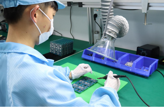
Component Placement and Soldering Defects: Common Errors and How to Avoid Them
Proper component placement and soldering are critical to ensuring that the PCB functions as intended. Common defects in component placement include misalignment, wrong component orientation, or incorrect part placement. Soldering defects, such as cold solder joints, solder bridges, or insufficient solder, can lead to faulty connections and even short circuits.
Example: In surface-mount technology (SMT), solder bridges can occur if too much solder is applied between adjacent pads. This can cause a short circuit, which may not be immediately visible but can result in malfunctioning devices. Automated soldering machines and careful inspection (e.g., using Automated Optical Inspection (AOI)) help minimize these issues.
Supply Chain Challenges: Component Shortages and International Shipping Delays
The global supply chain for PCB components is vulnerable to disruptions, such as component shortages, increased lead times, and shipping delays. These issues can cause delays in the PCB manufacturing process and lead to increased costs or production stoppages.
Example: If a specific semiconductor is in short supply, it can halt the entire assembly process, as the PCB cannot be completed without it. Manufacturers often mitigate this by maintaining a buffer stock of critical components or sourcing alternative components that meet the same specifications.
Navigating the complexities of PCB design and manufacturing requires a deep understanding of both technical and practical challenges. From ensuring signal integrity and managing trace routing to overcoming soldering defects and supply chain disruptions, every aspect of PCB production requires careful attention. By addressing these common challenges early in the design and manufacturing process, engineers can help ensure the production of high-quality, reliable PCBs that meet the performance needs of modern electronic devices.
Future Trends in PCB Design and Manufacturing
Innovations in PCB Design
The future of PCB design is being driven by breakthroughs in technology and material science, opening new possibilities for faster, more efficient, and highly customized PCBs. Here are some of the most promising innovations:
3D Printed PCBs: The Potential for Faster Prototyping and Custom Designs
3D printing is revolutionizing the way PCBs are designed and manufactured. Unlike traditional methods that require layering materials and etching traces, 3D printing allows for the rapid prototyping of complex designs in a fraction of the time. 3D printed PCBs can integrate both the substrate and the components, enabling custom, flexible designs for unique applications.
Example: For prototyping new consumer electronics, 3D printing allows designers to quickly test various designs without needing to go through the lengthy and costly process of traditional PCB fabrication.
Benefits: Faster design iterations, more complex designs, and cost savings for low-volume production.
Flexible and Stretchable PCBs: Applications in Wearable Tech and Medical Devices
Flexible PCBs are already being used in applications where traditional rigid PCBs wouldn’t fit, such as in wearable technology and medical devices. These flexible circuits can bend, twist, and fold, making them ideal for small, compact devices that need to fit into irregular shapes or move with the user’s body.
Example: A wearable health monitor could use a flexible PCB that conforms to the contours of the body, providing both comfort and reliability while continuously monitoring vital signs.
Stretchable PCBs, a more advanced version of flexible circuits, can even stretch and return to their original shape, making them suitable for applications in healthcare, electronics embedded in clothing, or soft robotics.
Example: Smart bandages with stretchable PCBs could monitor wounds in real-time, transmitting data to healthcare providers for continuous monitoring.
AI-Driven PCB Design: How Artificial Intelligence is Changing the Way We Design and Test PCBs
Artificial intelligence (AI) is beginning to play a significant role in PCB design and testing. AI tools can automate the design process, optimize component placement, and predict potential issues before they arise. Machine learning algorithms can analyze vast amounts of design data to identify the most efficient layouts, reducing design time and minimizing human errors.
Example: AI-based tools like Autodesk Eagle and Altium Designer are already helping engineers automatically optimize trace routing, component placement, and signal integrity for complex designs, all while learning from past designs to improve future iterations.
Benefits: Reduced design time, improved efficiency, and better predictive capabilities for error prevention and testing.
Sustainability in PCB Manufacturing
As environmental concerns become more urgent, the PCB industry is under increasing pressure to adopt sustainable practices. The future of PCB manufacturing will rely on green technologies and the development of eco-friendly materials to reduce environmental impact. Here are two major trends in sustainable PCB manufacturing:
Green PCB Manufacturing: Techniques to Reduce Waste and Energy Consumption
Green PCB manufacturing focuses on reducing the environmental impact of PCB production by using eco-friendly processes, recycling materials, and reducing energy consumption. Techniques like lead-free soldering, water-based chemicals, and solvent-free processes are already helping minimize toxic waste, while the development of more efficient production methods helps reduce energy use.
Example: The use of lead-free solder in PCB manufacturing is now standard practice, driven by regulations such as RoHS compliance. This reduces the environmental hazards associated with traditional lead-based soldering.
Benefits: Reduced waste, lower energy usage, and minimized environmental footprint.
Biodegradable Materials: Exploring the Future of Eco-Friendly PCBs
The next frontier in sustainable PCBs lies in the development of biodegradable materials. Researchers are exploring the use of bioplastics and other organic materials to create PCBs that decompose naturally, reducing electronic waste. These eco-friendly PCBs would not only be more sustainable to produce but would also reduce the environmental impact of discarded electronics.
Example: Biodegradable PCBs made from plant-based polymers or biodegradable resins could be used in devices like disposable medical sensors or environmentally friendly consumer electronics, where long-term durability is not required.
Benefits: Reduced environmental impact, less electronic waste, and the ability to recycle more materials at the end of the product’s lifecycle.
The future of PCB design and manufacturing is filled with exciting possibilities. Innovations like 3D printed PCBs, flexible and stretchable circuits, and AI-driven design tools are revolutionizing the industry, making it faster, more flexible, and more customized than ever before. At the same time, the push for sustainability is driving the development of green manufacturing processes and biodegradable materials, paving the way for more environmentally friendly electronic products. As these trends continue to evolve, they will shape the next generation of PCBs, enabling the development of smarter, more efficient, and eco-conscious technology.
Conclusion
PCB design and manufacturing are the backbone of modern electronics, enabling the development of everything from smartphones to medical devices. The complexity of PCB design, combined with advancements in materials and manufacturing techniques, ensures that these critical components remain at the heart of technological innovation. From signal integrity to component placement, every detail of the design must be precise to ensure functionality, reliability, and cost-effectiveness.
Looking ahead, future trends like 3D printed PCBs, flexible electronics, and AI-driven design will continue to shape the industry. These innovations promise faster prototyping, more customized solutions, and eco-friendly manufacturing, paving the way for smarter, more sustainable electronic products. At the same time, the push for green manufacturing and biodegradable materials highlights the industry's commitment to reducing its environmental footprint.
As the demand for high-performance PCBs grows, companies like PCBMASTER are well-positioned to meet these challenges, offering cutting-edge solutions that combine advanced design with sustainable practices. With these developments on the horizon, the future of PCB design and manufacturing holds exciting possibilities for both innovation and sustainability.
FAQs
What is the Difference Between Single-Sided, Double-Sided, and Multi-Layer PCBs?
Single-Sided PCBs: As the simplest type of PCB, a single-sided PCB has all its components mounted on one side, with traces and copper connections only on that side. These are typically used for low-cost applications like basic consumer electronics and devices with fewer components.
Use case: Simple electronics like calculators, basic household devices, and some low-cost gadgets.
Double-Sided PCBs: In a double-sided PCB, components and traces are placed on both sides of the board. This allows for a more compact design and is useful for more complex circuits without increasing the size of the PCB. Traces are connected through vias (small holes) that allow for electrical connections between both sides.
Use case: Devices with more complex circuits, such as power supplies, communication devices, and automotive electronics.
Multi-Layer PCBs: A multi-layer PCB has three or more layers of conductive material, separated by insulating layers. This design allows for a higher number of components and connections while keeping the overall size small. Multi-layer boards are commonly used in high-performance electronics and devices that require complex circuit layouts.
Use case: High-speed applications, like smartphones, computers, and advanced communication equipment.
How Do I Choose the Right Material for My PCB?
Choosing the right material for your PCB depends on several factors, including performance requirements, cost, and manufacturing capabilities. The most common PCB material is FR4, a fiberglass-reinforced epoxy resin, due to its balance of cost, durability, and insulating properties. However, other materials may be preferred for specific applications:
For high-frequency circuits, materials like PTFE (Teflon) or ceramic-filled resins are used because they have superior dielectric properties and minimize signal loss.
For flexible PCBs, polyimide is often the material of choice due to its ability to bend and maintain its electrical properties.
For environmentally-conscious designs, biodegradable PCBs made from plant-based polymers or other eco-friendly materials are emerging.
The key considerations in material selection are temperature tolerance, electrical performance, mechanical properties, and cost.
What Are the Advantages of Using Flexible PCBs Over Rigid PCBs?
Flexible PCBs offer several advantages over traditional rigid PCBs, particularly in applications where space-saving and flexibility are crucial:
Flexibility: Flexible PCBs can bend and conform to complex shapes, making them ideal for wearable devices, medical implants, and foldable electronics. Rigid PCBs, on the other hand, are fixed in shape and size.
Space Efficiency: Flexible PCBs can be folded, rolled, or twisted, which makes them useful in compact or constrained spaces.
Weight Reduction: Flexible PCBs are generally lighter than rigid boards, which is beneficial in applications like aerospace or mobile electronics.
Durability: Flexible circuits can withstand mechanical stress and vibration better than rigid PCBs, making them suitable for applications in dynamic environments.
However, rigid PCBs are still the preferred choice for many general-purpose electronics due to their stability, lower cost, and ease of manufacturing.
What Are the Key Considerations in Designing a PCB for High-Frequency Applications?
Designing a PCB for high-frequency applications, such as radio-frequency (RF) circuits, 5G communication devices, and high-speed digital circuits, requires careful attention to several critical factors:
Signal Integrity: High-frequency signals are sensitive to interference and loss. Proper trace routing and grounding are essential to maintain signal quality and minimize noise.
Impedance Control: The PCB must be designed to match the impedance of the circuit to ensure that signals are transmitted without reflection or signal loss. This is particularly important for high-speed digital and RF circuits.
Trace Lengths: Long traces can cause signal degradation or delay. In high-frequency designs, minimizing trace length and ensuring they are as direct as possible helps to preserve signal integrity.
Layer Stack-up: For multi-layer PCBs, choosing the right stack-up (the arrangement of signal and power layers) is crucial for maintaining controlled impedance and reducing signal interference.
Material Selection: High-frequency PCBs often require specialized materials like PTFE, ceramic, or low-loss laminates to ensure that signals are transmitted efficiently with minimal loss.
How Do Automated Optical Inspection (AOI) Systems Work in PCB Quality Control?
Automated Optical Inspection (AOI) is a non-contact, automated process used in PCB manufacturing to inspect the quality and integrity of the boards. AOI systems use high-resolution cameras to scan the PCB, comparing the actual image to a digital design file to identify any defects or inconsistencies. Here’s how the process works:
Inspection Process: The PCB is placed on a conveyor belt or inspection platform, and the AOI system captures detailed images of the board. These images are then analyzed by the software, which checks for common defects such as:
Misplaced components
Soldering defects (e.g., solder bridges, cold joints)
Component orientation issues
Missing or broken traces
Comparison with Design Files: The system compares the scanned PCB with the original design files (Gerber files), ensuring that everything is in the correct place and functioning as intended.
Defect Detection: If the system detects any deviations, it flags them for manual inspection or rework. This ensures that only high-quality PCBs proceed to the next stage of manufacturing or assembly.
Benefits: AOI enhances production efficiency, reduces the risk of human error, and ensures that defects are caught early in the process, preventing costly mistakes and improving overall product quality.

