


Why Use PCB Hybrid Construction? Benefits, Design Considerations, and Best Practices
Modern electronic systems are pushing PCB performance to new limits. As signal frequencies continue to rise and devices become more compact, designers are expected to deliver excellent signal quality, effective thermal management, high reliability, and competitive manufacturing costs—all within the same board.
However, relying on a single PCB material often creates trade-offs. A material that performs well for high-speed signal transmission may increase costs significantly, while a cost-effective substrate may struggle to meet demanding electrical or thermal requirements. As a result, PCB hybrid stack-up design has become an increasingly important solution for advanced applications such as 5G infrastructure, high-speed servers, radar systems, and high-power electronics.
By combining different materials within a single PCB, engineers can optimize performance where it matters most while maintaining overall design efficiency. Yet this approach also introduces new challenges related to material compatibility, manufacturing processes, and long-term reliability.
Understanding why hybrid PCB construction is used—and what design considerations must be addressed—is essential for building high-performance products successfully. The following sections explore the key benefits, technical challenges, and best practices behind PCB hybrid stack-up design.
What Is PCB Hybrid Lamination Design? How Is It Different from a Standard PCB?
PCB hybrid lamination design is a PCB manufacturing approach that combines different substrate materials in one stack-up to optimize performance and cost, whereas a standard PCB uses a single material (typically FR-4) throughout the entire board.
PCB Hybrid Lamination Design: Definition and Basic Principles
What Is a Hybrid PCB?
A hybrid PCB is a printed circuit board that combines two or more different substrate materials within the same stack-up. Instead of using a single material throughout the entire board, designers place specific materials only where their unique properties are needed.
For example, a high-frequency material may be used under RF signal traces, while standard FR-4 is used for power, control, and low-speed signal layers. This approach helps achieve better electrical performance without significantly increasing manufacturing costs.
In PCB manufacturing, hybrid PCB design is also called mixed-material PCB design , hybrid stack-up design , or PCB mixed lamination .
How Are Different Materials Combined in One PCB?
Different PCB materials are stacked together during the lamination process to form a single multilayer board.
A common method is to place specialized materials on critical signal layers while using FR-4 for the remaining layers. For example:
| Layer Function | Material |
| RF Signal Layer | Rogers Material |
| Ground Layer | FR-4 |
| Power Layer | FR-4 |
| Digital Signal Layer | FR-4 |
This structure allows high-speed or RF signals to benefit from low-loss materials while keeping the overall board cost under control.
The key principle is simple: use high-performance materials only where they provide measurable benefits.
What Is the Main Difference Between a Hybrid PCB and a Standard PCB?
The biggest difference is material selection.
A standard PCB uses the same substrate material throughout the entire board, most commonly FR-4. This simplifies manufacturing and reduces costs, but it may not meet the requirements of high-frequency or high-speed applications.
A hybrid PCB uses multiple materials with different electrical, thermal, or mechanical properties. Each material is chosen for a specific purpose.
| Feature | Standard PCB | Hybrid PCB |
| Material Type | Single Material | Multiple Materials |
| Cost | Lower | Moderate to Higher |
| High-Frequency Performance | Limited | Excellent |
| Thermal Management | Basic | Enhanced |
| Design Flexibility | Lower | Higher |
As electronic systems become faster and more complex, hybrid PCB stack-up design is increasingly used to balance performance, reliability, and cost.
Common PCB Hybrid Material Combinations
High-Frequency Material + FR-4
This is one of the most widely used hybrid PCB configurations.
Materials such as Rogers laminates are placed on RF or microwave signal layers, while FR-4 is used for non-critical layers. The high-frequency material reduces signal loss and improves impedance stability, while FR-4 keeps manufacturing costs reasonable.
This combination is commonly found in wireless communication equipment, antennas, and networking hardware.
PTFE Material + FR-4
PTFE (Polytetrafluoroethylene) , often known by the brand name Teflon, offers extremely low dielectric loss and excellent high-frequency performance.
In a PTFE + FR-4 hybrid PCB, PTFE is used for sensitive RF circuits, while FR-4 supports digital control and power distribution circuits.
For example, automotive radar systems operating at 77 GHz often use PTFE-based layers to maintain signal quality at very high frequencies.
The challenge with this combination is that PTFE and FR-4 have different mechanical properties, making lamination and drilling more complex.
Megtron Material + FR-4
Megtron materials , developed for high-speed digital applications, provide lower transmission loss than traditional FR-4.
A Megtron + FR-4 hybrid stack-up is commonly used in data centers, AI servers, and high-speed networking equipment where signal speeds can exceed 25 Gbps, 56 Gbps, or even 112 Gbps.
By using Megtron only on critical high-speed channels, manufacturers can achieve excellent signal integrity while avoiding the cost of building the entire PCB from premium materials.
Metal Core Material + FR-4
This hybrid structure combines a metal substrate, usually aluminum or copper , with traditional FR-4 layers.
The metal section quickly transfers heat away from high-power components, while FR-4 provides electrical routing and control circuitry.
A typical example is an industrial LED controller, where power devices generate significant heat but the control electronics do not require specialized thermal materials.
This design improves heat dissipation without adding unnecessary cost or weight.
Summary Table of Common PCB Hybrid Material Combinations
| Hybrid Material Combination | Key Properties | Main Function in PCB | Typical Applications | Key Challenge |
| High-Frequency Material + FR-4 (e.g., Rogers + FR-4) | Low signal loss, stable impedance, cost-efficient | RF/microwave layers use high-frequency material; FR-4 used for standard layers | Wireless communication equipment, antennas, networking hardware | Managing impedance consistency across mixed materials |
| PTFE Material + FR-4 | Extremely low dielectric loss, excellent RF performance | PTFE used for sensitive RF circuits; FR-4 for power and control | 77GHz automotive radar, high-end RF systems | Difficult lamination and drilling due to material mismatch |
| Megtron Material + FR-4 | Low transmission loss, supports ultra-high-speed signals | Megtron used for high-speed channels; FR-4 for general circuits | AI servers, data centers, high-speed networking (25–112 Gbps) | Cost control and precise signal integrity design |
| Metal Core Material + FR-4 | High thermal conductivity, strong heat dissipation | Metal layer for heat spreading; FR-4 for electrical routing | Industrial LED drivers, power electronics, motor control systems | Thermal expansion mismatch and structural complexity |
Which Applications Require PCB Hybrid Lamination Design?
5G Communication Equipment
5G systems often require hybrid PCB design because they operate at much higher frequencies than previous wireless technologies.
High-frequency signal paths need low-loss materials to reduce attenuation, while control and power circuits can still use FR-4.
Typical applications include:
- 5G base stations
- Massive MIMO antennas
- Small-cell communication equipment
- RF front-end modules
Without hybrid PCB construction, signal quality may degrade significantly at high frequencies.
High-Speed Servers and Data Center Equipment
Hybrid stack-ups are widely used in modern servers and networking systems.
As data rates increase, signal loss becomes a major challenge. Materials such as Megtron help maintain signal integrity over long trace lengths.
Common examples include:
- AI servers
- Cloud computing infrastructure
- High-speed switches
- Data center networking equipment
Hybrid designs allow critical channels to operate reliably while controlling overall PCB costs.
Millimeter-Wave Radar Systems
Millimeter-wave radar is one of the most demanding applications for hybrid PCB technology.
Radar frequencies often range from 24 GHz to 81 GHz, where ordinary FR-4 materials introduce excessive signal loss.
To maintain detection accuracy, radar signal layers typically use PTFE or other low-loss materials, while FR-4 supports power and processing circuits.
This design is commonly used in:
- Automotive ADAS radar
- Autonomous vehicle sensors
- Industrial positioning systems
RF Power Amplifier Systems
RF power amplifiers frequently use hybrid PCB materials.
These systems must handle both high-frequency signals and significant heat generation. As a result, designers often combine RF laminates with thermal management materials.
Benefits include:
- Lower signal loss
- Improved amplifier efficiency
- Better heat dissipation
- Longer product lifespan
Examples include wireless infrastructure amplifiers and satellite communication equipment.
High-Power Industrial Electronic Equipment
Hybrid PCBs are often used when thermal performance is as important as electrical performance.
Power converters, motor drives, and industrial control systems generate substantial heat during operation. Using metal-core materials only in high-temperature regions improves cooling while keeping the rest of the PCB cost-effective.
Common applications include:
- Industrial power supplies
- Motor control systems
- Renewable energy inverters
- High-power LED lighting systems
In these products, hybrid PCB design helps achieve a practical balance between thermal management, reliability, and manufacturing cost.
Why Design PCB Hybrid Boards? What Advantages Does Hybrid PCB Design Bring?
PCB hybrid boards are designed to combine different materials in one stack-up to optimize signal integrity, thermal performance, reliability, cost, and system integration flexibility in high-speed and high-power electronic applications.
Improving High-Frequency Signal Integrity
What is the main reason hybrid PCB improves signal quality?
Hybrid PCB improves signal quality by placing low-loss materials only in high-speed signal paths, which reduces signal attenuation and keeps impedance stable in high-frequency PCB design.
High-frequency limitations of FR-4 materials
FR-4 is widely used because it is cheap and easy to manufacture, but in high-frequency PCB applications above ~1GHz, it suffers from high dielectric loss and unstable dielectric constant (Dk) . This causes signal attenuation, jitter, and distortion. For example, in 10Gbps+ server signals, FR-4 alone can cause noticeable eye diagram closure.
Advantages of low dielectric constant (Dk) materials
Low-Dk materials such as Rogers laminates reduce signal delay and improve impedance control. A lower Dk means the signal travels faster and more predictably. For example, in RF PCB design, stable Dk helps maintain consistent antenna performance and reduces tuning effort.
Value of low-loss materials for high-speed transmission
Low-loss materials reduce insertion loss and keep signal energy intact over long PCB traces. This is critical in high-speed digital PCB design such as 56G PAM4 or 5G RF front-end circuits, where even small losses can affect system reliability.
How hybrid PCB separates high-speed and normal signals
Hybrid stack-up design places high-frequency materials only under RF or high-speed layers, while FR-4 is used for power and control layers. For example, a 5G base station PCB may use Rogers only for RF paths, while FR-4 handles digital control circuits, achieving both performance and cost efficiency.
Optimizing Thermal Performance
Why do localized high-heat areas need special design?
High-power components such as RF power amplifiers or power converters generate concentrated heat. Without proper thermal management, PCB overheating can cause performance drift or component failure.
Role of metal core and high-thermal-conductivity materials
Metal-core PCB materials (aluminum or copper base) quickly spread heat away from hot spots. In hybrid PCB thermal design, metal layers are only used where needed, improving cooling efficiency without making the entire board expensive.
How thermal management affects product stability
Stable temperature reduces electrical drift and mechanical stress. For example, in LED driver PCBs, poor thermal control can reduce brightness stability and shorten lifespan. Hybrid PCB improves long-term reliability by balancing heat distribution.
Application value in high-power electronic systems
In power electronics such as motor drives or DC-DC converters, hybrid PCB design allows thermal-sensitive power stages to be optimized separately from low-power control circuits, improving both efficiency and safety.
Improving Product Reliability
How thermal cycling affects PCB structure
Repeated heating and cooling causes materials to expand and shrink. In PCB hybrid materials, this mismatch can lead to stress accumulation, especially at layer interfaces.
Why CTE matching is critical
CTE (Coefficient of Thermal Expansion) mismatch between FR-4 and high-frequency materials can cause mechanical stress. Good PCB reliability design selects materials with similar Z-axis expansion to reduce deformation during thermal cycling.
Methods to reduce delamination risk
Delamination happens when layers separate due to weak bonding. Designers reduce this risk by using compatible prepregs, adding resin-rich bonding areas, and minimizing the number of different material systems in a single stack-up.
Methods to reduce via cracking risk
Via cracks occur when mechanical stress breaks plated holes. Hybrid PCB reliability improves by avoiding stacked vias in high-stress areas, using staggered vias, and optimizing via aspect ratio in high-CTE mismatch structures.
Reducing Overall Manufacturing Cost
Cost characteristics of high-performance materials
Materials like Rogers or PTFE are significantly more expensive than FR-4 due to complex manufacturing and strict performance requirements. This cost increases sharply when used across an entire PCB.
Cost issues of full high-frequency PCB solutions
Using only high-frequency materials for the entire board leads to unnecessary cost, especially for digital and power sections that do not require RF-grade performance.
Cost advantages of partial material usage
Hybrid PCB design applies expensive materials only to RF or high-speed signal layers. For example, in a 5G module, only antenna feed lines use Rogers while the rest uses FR-4, reducing material cost significantly.
How to balance performance and cost effectively
The key strategy is “use premium materials only where needed.” Designers evaluate signal criticality first, then assign materials based on electrical requirements, thermal needs, and budget constraints.
Meeting Complex Electronic System Design Requirements
Coexistence of high-speed and standard digital circuits
Modern systems often mix 56Gbps high-speed buses with low-speed control signals. Hybrid PCB allows different materials to support both without performance conflict.
RF and control circuit co-design on one board
In RF systems like radar modules, RF signal paths require low-loss materials, while control logic can remain on FR-4, enabling compact and integrated system design.
Multi-functional area material allocation
Hybrid PCB enables zone-based design, where each functional block (RF, power, digital) uses a tailored substrate to match its performance requirements.
Improving overall system design flexibility
By decoupling material selection from full-board constraints, engineers gain more freedom in layout, routing, and system integration. This is especially important in compact devices like automotive radar and 5G small cells.
What Material Compatibility Issues Should Be Focused on in PCB Hybrid Design?
PCB hybrid design must carefully manage compatibility issues between different materials, including mismatched thermal expansion (CTE), dielectric properties (Dk/Df) , mechanical behavior, and moisture absorption, as these differences directly affect signal integrity, structural reliability, and manufacturing yield.
Differences in Thermal Expansion (CTE) Between Materials
What is the main issue with CTE differences in PCB hybrid design?
The main issue is that different materials expand at different rates when heated, which creates mechanical stress inside the PCB during thermal cycling.
Impact of XY Direction Expansion
XY-direction expansion refers to how materials expand along the PCB surface during heating. In PCB hybrid stack-up design, FR-4 and high-frequency materials (like Rogers) may expand differently, causing layer misalignment or trace stress.
For example, in high-speed PCB manufacturing, even small XY mismatch can cause registration errors during lamination, leading to via misalignment or routing deviation.
Impact of Z-Axis Expansion on Via Reliability
Z-axis expansion affects the thickness direction of the PCB and directly impacts plated through-hole (PTH) reliability. When materials expand differently in the vertical direction, it can stress copper via walls and cause cracking.
For example, in multilayer hybrid PCBs used in 5G base stations, repeated heating cycles can lead to via barrel cracks if CTE mismatch is not controlled.
Differences in Dielectric Properties Between Materials
What is the key concern with dielectric mismatch?
The key concern is that inconsistent dielectric properties can distort signal behavior, especially in high-frequency and high-speed PCB design.
Dielectric Constant (Dk) Matching Issues
Dielectric constant (Dk) determines how fast signals travel through a material. In hybrid PCB design, mixing materials with different Dk values can cause signal delay differences and impedance discontinuity.
For example, a Rogers layer may have Dk ~3.0 while FR-4 may vary from 4.2–4.8, which affects controlled impedance routing in RF PCB design.
Dielectric Loss (Df) Matching Issues
Dielectric loss (Df) represents how much signal energy is lost as heat. If materials in the same signal path have different Df values, signal attenuation becomes uneven.
This is critical in high-speed digital PCB applications such as 56Gbps PAM4 links, where even small loss differences affect eye diagram quality.
Impedance Control Risks
Impedance control becomes unstable when different dielectric materials are mixed without proper stack-up design. This leads to signal reflection and transmission errors.
For example, in RF PCB antennas, impedance mismatch can reduce radiation efficiency and increase return loss (S11 degradation).
Differences in Mechanical Properties Between Materials
What is the main mechanical compatibility issue?
The main issue is that different materials have different stiffness and flexibility, which creates uneven stress during lamination and operation.
Rigidity vs Flexibility Differences
Some materials like FR-4 are rigid, while others like PTFE-based laminates are softer. When combined in PCB hybrid construction, this mismatch can lead to bending stress and uneven board warping.
For example, thin RF modules may warp after assembly if rigid and soft materials are not balanced properly.
Stress Issues During Lamination Process
During PCB lamination, high temperature and pressure are applied. If materials respond differently, internal stress builds up, which may cause delamination or micro-cracks.
A typical case is PTFE + FR-4 hybrid boards, where poor bonding can lead to layer separation if lamination parameters are not optimized.
Differences in Moisture Absorption Between Materials
Why is moisture absorption a problem in hybrid PCB?
Because different materials absorb moisture at different rates, which can cause swelling, delamination, and electrical instability.
Impact of Moisture on Reliability
Moisture trapped inside PCB layers can expand during soldering (reflow process), causing “popcorn effect” delamination or internal cracking.
For example, in automotive electronics, moisture-related failure is a known risk in hybrid PCB assemblies exposed to humid environments.
Impact of Moisture on High-Frequency Performance
Moisture changes dielectric properties, especially dielectric constant and loss. This leads to unstable RF performance and signal drift.
In millimeter-wave PCB design, even small humidity changes can affect antenna frequency tuning and reduce accuracy.
How to Select Better Material Combinations for Compatibility?
What is the key principle for material selection?
The key principle is to choose materials with similar physical and electrical behavior while minimizing the number of different material systems used.
Prefer Materials from the Same System
Using materials from the same manufacturer or same material family helps ensure similar CTE, Dk, and Df behavior.
For example, selecting a full Rogers-based system instead of mixing multiple unrelated laminates improves manufacturing stability.
Importance of Reducing Material Variety
Fewer materials mean fewer interfaces, which directly reduces the risk of delamination, warping, and impedance inconsistency.
In PCB hybrid stack-up design, reducing from four materials to two often significantly improves yield and reliability.
Material Selection Principles and Recommendations
A good hybrid PCB material selection strategy includes:
- Match CTE as closely as possible
- Keep dielectric constants consistent in signal paths
- Limit material types to essential functions only
- Validate stack-up through simulation before production
For example, in a 5G PCB, engineers often separate materials into only two groups: RF high-frequency material and standard FR-4, instead of using multiple mixed laminates.
How to Control Shrinkage and Warpage Risks in PCB Hybrid Boards?
Shrinkage and warpage risks in PCB hybrid boards can be controlled by optimizing material selection, using symmetric stack-up design, balancing copper distribution, applying accurate supplier shrinkage compensation data, and fine-tuning lamination processes to minimize internal stress between different materials.
What causes shrinkage and warpage in hybrid PCB manufacturing?
Shrinkage and warpage in PCB hybrid stack-up design are mainly caused by uneven material expansion during lamination and cooling, especially when FR-4 and high-frequency materials behave differently under heat and pressure.
In simple terms, each material “moves differently” when heated. When they are bonded together, internal stress builds up, which eventually leads to board bending (warpage) or size deviation (shrinkage). This is more obvious in high-layer-count hybrid PCBs used in 5G and server applications.
How does material shrinkage rate affect PCB fabrication accuracy?
Material shrinkage rate directly affects layer alignment and drilling precision in PCB manufacturing. If different materials shrink at different rates after lamination, the drilled vias may shift away from target pads.
For example, in high-speed PCB production, a 0.1% mismatch in shrinkage can cause via misregistration in dense BGA areas, leading to yield loss or electrical failure.
That is why PCB fabrication engineers always require material dimensional stability data before designing hybrid stack-ups.
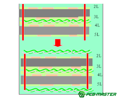
What are the design principles for symmetric stack-up structure?
The main principle is balance: materials and copper layers should be arranged symmetrically around the center of the PCB.
A symmetric PCB stack-up reduces internal stress because both sides of the board expand and contract equally during heating and cooling.
For example, a 10-layer hybrid PCB often mirrors layer structure like:
- Top signal layers = Bottom signal layers
- High-frequency layers placed symmetrically
- Copper distribution balanced left and right
This is a key PCB warpage control technique widely used in HDI and RF PCB design.
How should high-frequency materials be distributed in the stack-up?
High-frequency materials should be placed only where RF or high-speed signals exist, and should be distributed evenly to avoid unbalanced stress.
If all RF layers are placed on one side, the board will bend toward that side after lamination or reflow soldering.
A good PCB hybrid layout strategy is:
- Place RF layers near the center or symmetrically
- Avoid stacking all high-Dk materials on one side
- Keep FR-4 balanced on both sides
This improves both mechanical stability and RF signal integrity in high-frequency PCB design.
How are supplier shrinkage compensation parameters used?
PCB material suppliers provide shrinkage compensation factors that help predict how much a material will expand or shrink during processing.
Designers use these parameters to adjust Gerber scaling before fabrication, ensuring final PCB dimensions match the original design.
For example, if a high-frequency laminate has a known shrinkage of 0.2%, the PCB layout can be slightly pre-compensated so that after lamination, the final size is accurate.
This is especially important in multi-material hybrid PCB manufacturing where each material behaves differently.
What are common warpage problems and how can they be solved?
The most common PCB warpage issues include edge bending, center bulging, and diagonal twisting after lamination or reflow.
These problems are usually caused by uneven material stress, unbalanced copper distribution, or poor stack-up symmetry.
Common solutions include:
- Using symmetric stack-up design to balance stress
- Reducing material types in one board
- Increasing copper balance across layers
- Optimizing press temperature and pressure profiles
For example, in 5G base station PCBs, switching from an asymmetric RF stack-up to a symmetric hybrid design can significantly reduce post-lamination warpage and improve assembly yield.
In practice, warpage control is a combination of design optimization + material selection + process tuning in PCB hybrid manufacturing.
How to Solve Poor Interlayer Bonding in PCB Hybrid Boards?
Poor interlayer bonding in PCB hybrid boards can be solved by improving material compatibility, using surface treatments like plasma or chemical roughening, optimizing resin flow with mesh copper and flow channels, and validating adhesion through strict reliability testing such as thermal cycling and peel strength analysis.
What causes delamination in hybrid PCB stack-ups?
Delamination in PCB hybrid boards is mainly caused by weak adhesion between different materials during lamination, especially when FR-4 and high-frequency laminates have poor chemical and mechanical compatibility.
In simple terms, if the “glue strength” between layers is not strong enough, the board can separate under heat, pressure, or thermal cycling. This is a common PCB manufacturing reliability issue in high-frequency PCB and mixed-material stack-ups.
Why do PTFE and other high-frequency materials bond poorly?
PTFE-based materials (such as Teflon laminates) have very low surface energy, which means other materials like FR-4 prepreg cannot easily stick to them during PCB lamination.
For example, in RF PCB hybrid design, PTFE layers may show weak bonding after lamination if no surface treatment is applied. This can lead to edge lifting or internal separation after solder reflow.
To solve this, manufacturers often use special surface roughening or chemical treatment before bonding.
How does mesh copper design improve bonding strength?
Mesh copper (grid copper) improves interlayer adhesion by increasing mechanical interlocking between layers and allowing resin to flow more evenly during lamination.
In PCB hybrid stack-up design, solid copper planes can sometimes block resin flow, but mesh copper creates “anchor points” that help layers bond more tightly.
For example, in high-speed PCB designs, replacing large solid copper areas with mesh copper near interface layers can significantly reduce delamination risk.
What is the role of resin flow channels in improving adhesion?
Resin flow channels (also called flow grooves) are designed to guide epoxy resin during lamination so it can fully fill gaps between different materials.
These channels improve bonding strength by ensuring there are no air gaps or dry spots between layers.
However, in PCB hybrid manufacturing, designers must carefully control channel size—too large may weaken structure, too small may block resin flow. This is a common PCB stack-up optimization technique.
How are interface enhancement treatments applied to materials?
Interface enhancement methods improve bonding by modifying the surface of materials before lamination.
Common PCB surface treatment methods include:
- Plasma treatment to increase surface energy
- Chemical roughening for better mechanical grip
- Special bonding films or adhesion promoters
For example, in PTFE + FR-4 hybrid PCB production, plasma treatment is widely used to improve adhesion before lamination.
These methods help ensure stable long-term reliability in high-frequency PCB applications.
How do you verify interlayer bonding reliability?
Interlayer bonding reliability is verified through mechanical and thermal stress testing after PCB manufacturing.
Common PCB reliability tests include:
- Thermal shock testing (rapid heating and cooling cycles)
- Peel strength testing (measuring bonding force)
- Cross-section inspection (checking internal separation)
For example, in automotive radar PCB production, samples are often tested through multiple thermal cycles to ensure no delamination occurs under real operating conditions.
This verification step is critical in PCB hybrid design because it ensures the board can survive long-term use in high-power and high-frequency environments.
What Reliability Requirements Are Needed for Via Design in PCB Hybrid Boards?
Via design in PCB hybrid boards must ensure reliability by controlling thermal-stress-induced cracking through proper material compatibility, optimized via structures (preferably staggered over stacked), controlled aspect ratios, balanced high-density via layout, and strict process validation for multi-lamination manufacturing.
How do material differences affect via stress in hybrid PCB design?
Material differences in PCB hybrid stack-ups create uneven thermal expansion around vias, which generates mechanical stress on the plated copper barrel during heating and cooling cycles.
In simple terms, when FR-4 and high-frequency materials expand differently, the via hole “feels pulling forces” from different directions. Over time, this can weaken the copper plating and lead to cracking or open circuits in high-reliability PCB applications such as 5G and automotive radar.
Why is stacked via structure riskier in PCB hybrid design?
What reliability issues does stacked via structure have?
Stacked vias are more vulnerable because multiple via layers are directly aligned on top of each other, concentrating mechanical and thermal stress in a single vertical path.
This structure increases the risk of:
- Copper barrel cracking under thermal cycling
- Misalignment between layers during lamination
- Stress concentration at via junction points
For example, in high-speed PCB manufacturing, stacked vias in hybrid materials often fail earlier than staggered vias when exposed to repeated solder reflow cycles.
When is stacked via structure acceptable in PCB design?
Stacked vias can still be used in HDI PCB designs where space is extremely limited, such as smartphone or compact RF modules.
However, they require:
- Careful control of aspect ratio
- High-quality electroplating process
- Strict thermal reliability testing
In most PCB hybrid stack-up designs, engineers avoid stacked vias unless absolutely necessary.
What are the advantages of staggered via design?
Staggered vias improve reliability by distributing stress across multiple offset holes instead of concentrating it in one vertical line.
This design reduces:
- Thermal stress concentration
- Mechanical fatigue risk
- Probability of via cracking
For example, in 5G base station PCBs, staggered via structures are commonly used to improve long-term durability under high-frequency and high-temperature conditions.
What are the thickness-to-diameter (aspect ratio) control principles for vias?
The via aspect ratio is the ratio of PCB thickness to hole diameter, and it directly affects plating quality and mechanical strength.
A general PCB reliability rule is:
- Lower aspect ratio = better plating quality
- Higher aspect ratio = higher risk of voids or cracks
In PCB hybrid designs, engineers typically keep aspect ratios within manufacturable limits (e.g., 8:1 or lower depending on the process capability) to ensure reliable copper deposition and reduce failure risk in high-density interconnect (HDI) boards.
What design recommendations apply to high-density via regions?
High-density via areas require careful spacing and thermal balance to avoid stress concentration and electrical interference.
Key PCB design recommendations include:
- Avoid clustering too many vias in a small area
- Maintain sufficient spacing between adjacent vias
- Balance copper distribution around via fields
- Use thermal relief patterns when connected to large planes
For example, in AI server PCB designs, via fields under BGA components are carefully optimized to prevent heat buildup and mechanical stress during operation.
How to control via reliability in multi-lamination PCB structures?
Multi-lamination PCB structures increase manufacturing complexity because each lamination cycle introduces additional thermal and mechanical stress on existing vias.
To improve reliability, engineers should:
- Minimize the number of lamination cycles when possible
- Use high-quality bonding materials for each layer interface
- Ensure via filling or reinforcement in early stages
- Perform step-by-step reliability validation after each build-up stage
For example, in 1+N+1 HDI hybrid PCB structures, via reliability is controlled by combining sequential lamination with strict inspection after each pressing cycle.
This approach is widely used in high-end RF and high-speed PCB manufacturing to ensure long-term stability under thermal cycling and vibration conditions.
What Special Process Requirements Are Needed in PCB Hybrid Manufacturing?
PCB hybrid manufacturing requires specialized drilling, material-specific desmear and surface activation (such as plasma for PTFE), controlled electroplating, RF-area protection, and tightly managed process parameters to ensure consistent quality and high yield across different materials.
What challenges does drilling face in PCB hybrid processing?
Drilling in PCB hybrid manufacturing is difficult because different materials have different hardness, elasticity, and thermal response, which affects drill bit wear and hole accuracy.
In simple terms, the drill “feels different resistance” when passing through FR-4, PTFE, or high-frequency laminates. This can cause issues like hole wall roughness, misalignment, or uneven hole diameter in high-precision PCB drilling processes.
For example, in high-speed server PCB production, mixed-material stacks often require adjusted drilling parameters to maintain consistent via quality.
What are the special requirements for PTFE drilling debris (smear) removal?
PTFE materials produce drilling smear that is chemically resistant and difficult to remove using standard desmear processes used for FR-4.
The main issue is that PTFE debris can block copper plating adhesion inside vias, leading to weak electrical connections or via failure in RF PCB manufacturing.
Therefore, special pre-treatment methods such as plasma activation or optimized mechanical drilling parameters are required to ensure clean via walls in PTFE-based hybrid PCB designs.
When to choose plasma cleaning vs chemical desmear?
Plasma cleaning is preferred when working with chemically inert materials like PTFE, while chemical desmear is more effective for standard FR-4 materials.
Plasma cleaning improves surface energy and activates bonding surfaces without damaging sensitive high-frequency materials. In contrast, chemical desmear uses strong oxidizing agents that may degrade PTFE surfaces.
For example, in RF PCB hybrid stack-ups, manufacturers often use plasma cleaning for PTFE layers and chemical desmear for FR-4 layers in a combined process flow.
How does electroplating affect hybrid PCB reliability?
Electroplating quality directly affects via strength and conductivity in PCB hybrid boards because uneven material surfaces can lead to poor copper deposition.
If plating is not uniform, vias may develop voids, weak copper walls, or high resistance areas, which can fail under thermal stress in high-reliability PCB applications.
For example, in 5G base station PCBs, poor plating in hybrid stacks can significantly reduce long-term signal stability and increase field failure rates.
What protection measures are needed for high-frequency PCB areas?
High-frequency areas in PCB hybrid design must be protected from contamination, mechanical damage, and process-induced variation during manufacturing.
Common protection measures include:
- Using cover films or protective masks during drilling and plating
- Isolating RF-sensitive areas from aggressive chemical processes
- Controlling tool paths to avoid damaging fine RF traces
For example, in millimeter-wave radar PCB production, RF signal regions are often isolated to prevent surface damage that could affect impedance and signal loss.
What are the key factors for improving PCB hybrid manufacturing yield?
Yield control in PCB hybrid manufacturing depends on stabilizing processes that are sensitive to material differences and multi-step lamination.
Key focus areas include:
- Stable drilling parameters across different materials
- Proper desmear and surface activation processes
- Controlled plating thickness and uniformity
- Strict inspection after each key manufacturing stage
For example, in AI server PCB production, manufacturers often use step-by-step inspection (drill → desmear → plating → lamination) to detect defects early and improve final yield.
In practice, hybrid PCB yield improvement is achieved by combining process optimization + material-specific handling + strict quality control systems .
How to Choose the Right Surface Finish for PCB Hybrid Boards?
The right surface finish for PCB hybrid boards should be selected based on functional zones, using low-loss finishes like immersion silver for RF/high-frequency areas, ENIG for reliable digital or mixed-signal regions, and immersion tin for cost-sensitive power or low-frequency sections to balance performance, reliability, and cost.
What are the advantages and limitations of ENIG (Electroless Nickel Immersion Gold)?
ENIG is one of the most commonly used surface finishes in PCB hybrid design because it provides excellent corrosion resistance, flat surface quality, and good solderability.
However, its main limitation is cost and potential reliability issues in high-frequency applications. The nickel layer can slightly affect RF performance, and process instability may cause defects such as uneven gold thickness.
For example, in 5G base station PCBs, ENIG is widely used for digital and control areas, but sometimes avoided in critical RF signal paths due to performance sensitivity.
What is black pad risk in high-frequency PCB applications?
Black pad is a reliability defect in ENIG surface finish caused by excessive phosphorus in the nickel layer, which leads to weak solder joints and long-term connection failure.
In PCB hybrid RF design, black pad risk becomes more critical because it can cause intermittent failures in high-frequency signal paths.
For example, in server PCB assemblies, black pad issues may lead to hidden solder joint failures that only appear after thermal cycling in field operation.
When should ENIG be used in PCB hybrid design?
ENIG is suitable for applications that require high reliability, fine-pitch assembly, and long shelf life.
Typical use cases include:
- High-density interconnect (HDI) PCBs
- BGA and fine-pitch component assembly
- Industrial control boards
- Mixed-signal PCB regions (non-RF areas)
In hybrid PCB stack-ups, ENIG is often applied to digital and power sections rather than sensitive RF signal layers.
When is immersion silver used in PCB manufacturing?
Immersion silver is widely used in high-frequency PCB applications because it offers low signal loss and excellent conductivity.
It is commonly used in:
- RF PCB modules
- 5G communication equipment
- High-speed digital interfaces
- Millimeter-wave antenna boards
For example, in 77GHz automotive radar PCBs, immersion silver is often selected because it provides better RF performance than ENIG.
However, it requires good storage control because silver can tarnish over time.
When is immersion tin used in PCB hybrid designs?
Immersion tin is suitable for cost-sensitive PCB applications where good solderability is needed but ultra-high-frequency performance is not critical.
It is commonly used in:
- Consumer electronics
- Power management PCBs
- Low- to mid-frequency digital boards
In PCB hybrid design, immersion tin may be applied to power or control sections, while RF areas use higher-performance finishes.
Its main advantage is low cost, but it has weaker oxidation resistance compared to ENIG or silver.
How do surface finishes affect RF performance in hybrid PCBs?
Different surface finishes affect RF performance by changing signal loss, impedance stability, and surface conductivity.
For example:
- ENIG adds a nickel layer that slightly increases signal loss
- Immersion silver provides very low RF insertion loss
- Immersion tin offers moderate performance but higher loss than silver
In high-frequency PCB design above 10GHz, even small differences in surface roughness and conductivity can affect antenna efficiency and return loss (S11).
How should surface finishes be selected in PCB hybrid design?
The best strategy is to match surface finish type with functional zones of the PCB.
A practical selection approach is:
- RF/high-frequency areas → immersion silver or optimized ENIG
- Digital/control areas → ENIG for reliability
- Power/low-frequency areas → immersion tin for cost efficiency
For example, in 5G hybrid PCB stack-ups, engineers often combine silver for RF traces and ENIG for control circuits to balance performance, cost, and reliability.
The key principle is simple: use the best-performing finish only where signal sensitivity requires it, not across the entire board.
How to Improve Manufacturability and Reduce Production Risk in PCB Hybrid Boards?
Manufacturability and production risk in PCB hybrid boards can be improved by simplifying material selection, standardizing stack-up designs, ensuring early DFM review, confirming manufacturer capability in materials and processes, and managing procurement and reliability requirements from the design stage.
What makes PCB hybrid manufacturing difficult?
PCB hybrid manufacturing is difficult because it combines different materials in one stack-up, and each material behaves differently during lamination, drilling, and thermal processing.
In simple terms, the PCB factory must “control multiple materials at the same time,” such as FR-4, PTFE, and high-frequency laminates. These materials have different expansion rates, bonding behavior, and processing requirements, which increases the risk of warpage, delamination, and yield loss in PCB hybrid stack-up production.
How to manage procurement cycles for special PCB materials?
Special materials like Rogers, PTFE, or Megtron often have long lead times and limited supplier availability, which can delay PCB production schedules.
The key is early material planning in PCB design, including:
- Confirming supplier lead time before final design
- Avoiding rare or low-stock material combinations
- Standardizing commonly used laminate types
For example, in 5G PCB manufacturing projects, delays often occur because high-frequency materials are not stocked locally, requiring 2–6 weeks of procurement time.
Why is reducing material variety important in hybrid PCB design?
Reducing material types simplifies manufacturing and improves yield because fewer materials mean fewer compatibility problems.
Each additional material increases risks such as:
- Different thermal expansion behavior
- More complex lamination cycles
- Higher probability of delamination
For example, a PCB using only FR-4 + one high-frequency material is much more stable than a design mixing three or four different laminate systems. This is a key rule in PCB hybrid stack-up optimization.
What is standard stack-up design strategy in PCB hybrid boards?
Standardized stack-up design means using repeatable, proven layer structures instead of fully customized layouts for every project.
This improves manufacturability because PCB factories can reuse validated processes, including:
- Known lamination pressure profiles
- Established drilling parameters
- Proven impedance control rules
For example, many high-speed PCB manufacturers use fixed “8-layer or 10-layer reference stack-ups” for hybrid designs to reduce engineering risk and shorten production time.
What should be checked in DFM (Design for Manufacturability) review?
DFM review ensures that the PCB design can actually be manufactured with high yield and low risk.
Key PCB hybrid DFM checks include:
- Material compatibility validation
- Via structure feasibility (stacked vs staggered)
- Minimum drill size and spacing
- Copper balance and symmetry
- Lamination cycle limitations
For example, in RF PCB production, DFM review often catches issues like excessive stacked vias or unbalanced copper layers that would otherwise cause warpage or yield failure.
What should be confirmed with PCB manufacturers during the design stage?
Early communication with PCB manufacturers is critical in hybrid PCB projects to avoid production delays and technical failures.
Material inventory availability
Confirm whether the PCB factory has stock or supply access to required materials such as Rogers, PTFE, or Megtron.
If materials are unavailable, redesign may be needed to avoid long lead times or cost increases.
Lamination process capability
Different hybrid PCB stack-ups require specific lamination pressure and temperature profiles.
Designers must confirm:
- Maximum layer count capability
- Compatible material combinations
- Press cycle limits
For example, not all PCB factories can handle multi-material RF + FR-4 hybrid lamination reliably.
Drilling and plating capability
Hybrid PCBs require precise drilling and high-quality via plating due to different material hardness.
Key confirmations include:
- Minimum drill diameter capability
- Aspect ratio limits
- Desmear process compatibility (especially for PTFE materials)
This directly affects via reliability in high-speed PCB designs.
Reliability testing requirements
Reliability standards must be agreed early to ensure the product meets field performance expectations.
Common tests include:
- Thermal cycling tests
- Peel strength testing
- Electrical continuity testing after stress
For example, automotive and 5G PCB projects often require stricter reliability validation compared to consumer electronics, making early agreement essential.
How to Design Highly Reliable PCB Hybrid Stack-Up Structures?
Highly reliable PCB hybrid stack-up structures are designed by strategically placing high-frequency materials only in critical signal paths, balancing power and ground layers, using symmetric layer configurations, carefully controlling material thickness, and validating proven stack-up architectures to ensure signal integrity, thermal stability, and mechanical reliability.
What are the basic principles of hybrid PCB stack-up design?
The basic principle of PCB hybrid stack-up design is to match each functional requirement with the most suitable material while keeping the overall structure balanced and manufacturable.
In simple terms, designers should not “overuse expensive materials,” but instead assign high-frequency materials only to critical signal paths and use FR-4 for power and control areas. This improves PCB hybrid reliability, reduces cost, and maintains stable electrical performance.
Key principle: function-driven material allocation + balanced mechanical structure.
How should high-frequency layers be positioned in a PCB stack-up?
High-frequency layers should be placed close to signal-critical components and ideally near the center of the stack-up to reduce interference and improve signal stability.
In RF PCB design, placing high-frequency layers in symmetrical positions helps reduce signal loss and electromagnetic noise. For example, in 5G PCB stack-ups, RF layers are often placed in inner layers to shield them from external interference.
Good placement improves:
- Signal integrity
- EMI performance
- Controlled impedance accuracy
How should power and ground layers be configured?
Power and ground layers should be placed adjacent to each other to create strong decoupling capacitance and stable return paths for high-speed signals.
In PCB hybrid stack-up design, continuous ground planes are critical because they provide a low-impedance return path and reduce noise coupling between layers.
For example, in high-speed server PCBs, alternating power and ground layers helps maintain stable voltage distribution and reduces signal jitter.
What are the rules for symmetric stack-up design?
Symmetric stack-up means both sides of the PCB have similar layer structure, copper distribution, and material thickness to balance internal stress.
This is important in hybrid PCB manufacturing because different materials expand differently under heat. If the structure is not balanced, the board may warp during lamination or reflow.
Example rule:
- Top half structure = Bottom half structure
- Copper weight balanced on both sides
- High-frequency materials placed symmetrically
This greatly improves PCB warpage control and long-term reliability.
How should different material thicknesses be assigned?
Material thickness should be assigned based on electrical performance, impedance control, and mechanical stability requirements.
In PCB hybrid design:
- High-frequency layers use thinner dielectric for better impedance control
- FR-4 layers provide mechanical strength and support
- Total stack-up thickness must remain uniform and manufacturable
For example, in RF PCB designs, thinner dielectric layers help achieve precise 50Ω impedance for microwave signals.
Typical PCB Hybrid Stack-Up Case Studies
4-layer high-frequency hybrid PCB design example
In a 4-layer hybrid PCB, the structure is typically:
- Top layer: RF signal (Rogers material)
- Inner layer: Ground (FR-4 or mixed)
- Inner layer: Power (FR-4)
- Bottom layer: Control signals (FR-4)
This design is commonly used in small RF modules where cost control and signal integrity must be balanced, such as IoT wireless devices.
8-layer high-speed server PCB design example
In an 8-layer PCB hybrid stack-up:
- High-speed signal layers use low-loss materials (Megtron or similar)
- Inner layers are dedicated to power and ground planes
- Outer layers handle control and routing
This structure is widely used in AI servers and data center switches where signal speeds exceed 25–56 Gbps.
Key advantage: stable impedance + low insertion loss + thermal stability.
1+N+1 HDI hybrid PCB design example
The 1+N+1 HDI structure combines sequential lamination with microvias for high-density routing.
Typical configuration:
- Outer HDI layers for fine-pitch components
- Core layers using FR-4 or mixed materials
- High-frequency materials used only in critical signal zones
This design is commonly used in smartphone modules, automotive radar, and compact RF systems where space and performance are both critical.
Key benefit: high routing density with controlled signal integrity and improved reliability.
What Evaluation and Verification Work Must Be Done Before PCB Hybrid Design?
Before PCB hybrid design, engineers must complete system requirement definition, material compatibility evaluation, signal loss and impedance analysis, thermal and reliability risk assessment, and multi-physics simulations (SI/PI/thermal/mechanical) to ensure performance, manufacturability, and long-term stability.
Why is system performance requirement analysis necessary?
System performance requirement analysis defines what the PCB must achieve before any material or stack-up design begins.
In simple terms, it answers: “What is this PCB expected to do?” For PCB hybrid design, this includes signal speed, operating frequency, power levels, and environmental conditions.
For example, a 5G base station PCB requires high-frequency signal integrity above 28 GHz, while an AI server PCB focuses more on 56 Gbps high-speed data transmission. Without clear requirements, material selection and stack-up design may be incorrect from the start.
How to evaluate feasibility of PCB material selection?
Material feasibility evaluation checks whether selected materials (FR-4, Rogers, PTFE, Megtron, etc.) can realistically meet electrical, thermal, and manufacturing requirements.
The key point is compatibility: not all materials can be reliably combined in PCB hybrid stack-up design due to differences in CTE, bonding behavior, and processing conditions.
For example, mixing too many laminate systems increases the risk of delamination and warpage. A good practice is to limit material types and choose compatible material families.
Why is high-speed signal loss analysis important?
High-speed signal loss analysis measures how much signal energy is lost during transmission across PCB traces.
In high-speed PCB design, materials with high dielectric loss (Df) can weaken signals, especially at frequencies above 10–25 GHz.
For example, in 56 Gbps server backplanes, excessive insertion loss can cause eye diagram closure, leading to data errors. This analysis ensures the selected hybrid materials can maintain signal quality over distance.
What is impedance control verification in PCB design?
Impedance control verification ensures that signal traces maintain a consistent electrical impedance (e.g., 50Ω or 100Ω differential) across different materials.
In PCB hybrid stack-up design, different dielectric constants (Dk) make impedance harder to control, so precise stack-up modeling is required.
For example, RF PCB antenna feeds must maintain stable impedance to avoid signal reflection and reduce return loss (S11 degradation).
Why is thermal management requirement evaluation needed?
Thermal management evaluation ensures the PCB can safely dissipate heat generated by high-power components.
In hybrid PCB design, different materials have different thermal conductivity, which affects heat flow across the board.
For example, power amplifier circuits in RF systems can generate significant heat, requiring metal-core or high-thermal materials in specific regions to prevent overheating and performance drift.
What does reliability risk assessment include?
Reliability risk assessment identifies potential long-term failure mechanisms such as delamination, via cracking, and thermal fatigue.
In PCB hybrid structures, risks are higher due to material mismatch between FR-4 and high-frequency laminates.
For example, repeated thermal cycling in automotive electronics can cause micro-cracks in vias if CTE mismatch is not properly controlled.
What Simulation and Validation Work Is Required?
Why is simulation important in PCB hybrid design?
Simulation helps predict real-world PCB behavior before manufacturing, reducing costly design failures.
It allows engineers to test signal performance, power stability, heat distribution, and mechanical stress in a virtual environment.
What is SI (Signal Integrity) simulation used for?
Signal Integrity (SI) simulation analyzes how well high-speed signals travel through PCB traces without distortion.
It evaluates:
- Signal reflection
- Crosstalk between traces
- Eye diagram quality
For example, in 25–56 Gbps high-speed PCB design, SI simulation ensures that hybrid materials do not degrade signal clarity.
What is PI (Power Integrity) simulation?
Power Integrity (PI) simulation checks whether the power delivery network provides stable voltage to all components.
It focuses on:
- Voltage drop across power planes
- Noise in power distribution
- Decoupling capacitor effectiveness
In AI server PCB design, PI simulation ensures stable power supply during sudden load changes.
What is thermal simulation in PCB design?
Thermal simulation models how heat moves through the PCB during operation.
It identifies:
- Hot spots on the board
- Heat dissipation efficiency
- Temperature distribution across materials
For example, in power electronics PCB design, thermal simulation helps determine whether metal-core regions are needed.
What is structural stress analysis in PCB hybrid boards?
Structural stress analysis evaluates mechanical deformation caused by thermal expansion, pressure, and material mismatch.
It focuses on:
- Warpage risk
- Delamination probability
- Via and layer stress points
For example, in multi-layer hybrid PCB manufacturing, stress simulation helps prevent bending during lamination and reflow soldering processes.
Conclusion
PCB hybrid design is ultimately about making smart trade-offs between performance, reliability, thermal behavior, and cost. When different materials are combined in a single stack-up, every decision—from layer structure to material selection and process control—directly affects signal integrity and long-term stability. That is why careful planning, simulation, and manufacturability validation are essential before moving into production.
At the same time, real-world success does not depend on design alone. It also relies on how well the design is translated into manufacturing. Close collaboration with an experienced PCB partner helps reduce risk, improve yield, and ensure that complex hybrid structures are built as intended.
PCBMASTER, as a seasoned PCB and PCBA supplier , specializes in advanced PCB technologies including hybrid stack-up design, high-frequency boards, and high-reliability manufacturing solutions. With strong engineering support and mature production capabilities, PCBMASTER helps bridge the gap between design intent and stable mass production.
As a result, engineers can focus more on innovation, while production challenges are handled with confidence and precision.
FAQs
Is a PCB hybrid board always more expensive than a standard FR-4 board?
No, a PCB hybrid board is not always more expensive. The cost depends on how much high-performance material is used and where it is applied. If expensive materials like Rogers or PTFE are used only in critical signal areas, while the rest uses FR-4, the overall cost can be controlled. In many cases, hybrid design is actually a cost optimization strategy rather than a cost increase.
Does high-frequency material need to cover the entire PCB?
No, high-frequency materials do not need to cover the entire PCB. They are only required in signal paths where high-speed or RF performance is critical. Non-sensitive areas such as power distribution or control circuits can still use FR-4. This selective usage is a core principle of PCB hybrid stack-up design.
Can a hybrid PCB use more than three types of materials?
Yes, but it is generally not recommended. While technically possible, using more than three material systems increases manufacturing complexity, cost, and reliability risks such as delamination and warpage. Most practical PCB hybrid designs use two materials, or at most three in highly specialized applications.
Is a hybrid PCB more prone to warpage and delamination?
Yes, hybrid PCBs have a higher risk of warpage and delamination compared to single-material FR-4 boards because different materials expand, contract, and bond differently under heat and pressure. However, this risk can be controlled through symmetric stack-up design, proper material selection, and optimized lamination processes.
Should material selection or stack-up design come first in hybrid PCB design?
Stack-up design should come first. The electrical and structural requirements of the system define the layer architecture, and then materials are selected to match each functional layer. Choosing materials first can lead to design constraints and suboptimal performance in PCB hybrid structures.
Why should PCB hybrid projects be discussed with the manufacturer early?
Early communication with the PCB manufacturer ensures that the chosen materials, stack-up design, and process requirements are manufacturable. It helps avoid issues such as unavailable materials, incompatible lamination cycles, or drilling limitations, which can otherwise cause delays, redesigns, or yield loss.
When is PCB hybrid design not necessary?
PCB hybrid design is not necessary when the product operates at low frequencies, has simple signal requirements, or cost sensitivity outweighs performance needs. In typical low-speed digital circuits, consumer electronics, or basic control boards, standard FR-4 is usually sufficient without introducing hybrid complexity.
About the Author

Carol Luo
PCB Design EngineerI'm Carol, a PCB Engineer at PCBMASTER with experience in PCB design and manufacturing engineering since 2018. I focus on translating engineering requirements into reliable PCB solutions, with expertise in stack-up design, material selection, and design-for-manufacturing (DFM). I share practical engineering insights from real-world PCB design and production experience.
Visit Carol Luo's Profile
