


Understanding Plated Through Hole PTH Fill Techniques and Benefits
Introduction
In the world of electronics manufacturing, the quality of those tiny holes determines the life or death of a product.
Plated Through-Hole (PTH) solder fill, often referred to as solder wick-up or hole fill, is a crucial process step in PCB Assembly (PCBA). It directly impacts the reliability and lifespan of the circuit board. Whether for consumer electronics, automotive systems, or aerospace equipment, the quality of solder fill is a key factor influencing product performance. This article serves as a comprehensive guide to plated through hole PTH fill techniques and benefits.
What is Plated Through-Hole Solder Fill?
In simple terms, PTH solder fill describes the process in Through-Hole Technology where molten solder, driven by capillary action and influenced by surface tension, rises completely from the solder side of the printed circuit board (PCB) through the gap between the component lead and the via hole or plated hole barrel, reaching the component side. The process begins with the drill step, where holes are drilled through the PCB, including its internal layers and inner layers. These holes are then processed through several manufacturing steps: drill, clean, hole plating (where a conductive layer is deposited inside the via hole during the plate process), fill, and inspect. The average thickness of the plating layer inside the hole is typically 0.0009 - 0.001 inches, which is important for electrical conductivity and fit. The hole size and aspect ratio are critical design considerations to ensure effective filling and plating.
There are two types of PTH holes: those filled with conductive material and those filled with non conductive material. The filling process can use either, depending on the application, to enhance current carrying capacity or provide structural support. After plating, the via holes can be filled (using conductive or non conductive material) to meet reliability standards such as type vii. The copper pad or pad is the area where the component lead connects, and the fill ensures a robust electrical and mechanical connection between the lead and the plated hole wall. In contrast, non plated holes do not have this conductive plating and are not used for electrical connections.
A via can connect one layer to the other side or multiple layers within the PCB, depending on the design. The filled via holes are then ready for automated assembly, where components are placed and soldered efficiently.
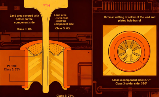
Fill quality is typically measured by the solder fill ratio, which is the height of the solder in the through-hole compared to the PCB thickness. According to IPC standards, acceptable through-hole solder fill for PCBA often requires greater than 75%. This means the solder must fill at least 75% of the hole’s vertical height (board thickness) as a minimum acceptability criterion for many classes of electronics.
Why is Solder Fill So Critical?
Good solder fill quality is vital for the reliability of electronic products:
·Enhances Mechanical Strength: Adequate solder fill provides superior grip and fatigue resistance for component leads, and proper fill also offers structural support to both the component lead and the PCB. Even under vibration or shock, components are less likely to become loose or detach.
·Ensures Electrical Reliability: Complete solder fill guarantees a 360-degree bond between the component lead and the through-hole wall, maximizing the conductive cross-section and ensuring stable, long-term current transfer. This also maximizes the current carrying capacity of the connection.
·Prevents Quality Defects: Poor solder fill can easily lead to issues like cold solder joints, solder cracks, or even component detachment. The choice of conductive material or non conductive material for fill can impact reliability, as these defects are often latent, meaning they may not be detected during initial testing but can cause critical failures during the product’s operational life.
Benefits of Using PTHs in PCBs
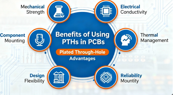
Plated through holes (PTHs) are a foundational element in the construction of modern printed circuit boards, offering a host of advantages that make them indispensable in today’s electronics industry. One of the most significant benefits of PTHs is their ability to establish reliable electrical connections between different layers of a circuit board. The copper plating inside each plated hole forms a continuous, conductive path, ensuring robust electrical connectivity for signal paths and power distribution across various layers.
Beyond electrical connection, PTHs contribute greatly to the mechanical strength of circuit boards. By anchoring component leads securely within the hole barrel, plated through holes help distribute mechanical stress, especially in areas where connectors, switches, or other through hole components are subject to repeated use or vibration. This robust structure minimizes the risk of solder joint failure and enhances the overall durability of the board.
Thermal management is another area where PTHs excel. The copper plating within the holes acts as a conduit for heat, allowing thermal energy to dissipate efficiently from heat-generating components to other parts of the board or to external heat sinks. This improved thermal conductivity helps prevent overheating, which is critical for maintaining the performance and longevity of sensitive integrated circuits and passive components.
Signal integrity is also enhanced by the use of plated through holes. By providing a direct, low-resistance path for electrical signals, PTHs reduce the likelihood of signal degradation, crosstalk, or distortion—factors that are especially important in high-speed or high-frequency PCB designs. The consistent plating thickness and quality of the metal coating inside the holes ensure stable electrical performance across all signal paths.
From a manufacturing perspective, the PTH process—encompassing drilling, electroless copper deposition, and subsequent copper plating—can be efficiently integrated into automated PCB fabrication workflows. This streamlines production, reduces manual labor, and helps maintain consistent quality across large volumes of boards. The use of liquid photo imageable (LPI) solder mask and immersion silver or other surface finishes further enhances the reliability and performance of the finished product.
Cost-effectiveness is another key advantage. While the initial steps of drilling and plating holes add to the manufacturing process, the long-term benefits—such as reduced need for additional interconnects, improved reliability, and fewer field failures—can significantly lower the overall cost of ownership. PTHs also offer design flexibility, accommodating a wide range of component types and allowing for complex multi-layer PCB designs that meet the demands of advanced electronic systems.
In summary, plated through holes provide essential benefits in terms of electrical connectivity, mechanical strength, thermal management, and signal integrity, all while supporting cost-effective and flexible PCB manufacturing. By leveraging the strengths of PTH technology, designers and manufacturers can create high-performance, reliable circuit boards that stand up to the challenges of modern electronics.
Key Factors Influencing Solder Fill Quality
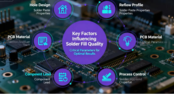
Material Factors
Molten tin possesses strong fluidity and penetration capabilities at high temperatures, but its ability to wet and flow depends on the surface condition of the metals being joined (PCB and component leads). Surface tension also plays a crucial role in how well the solder wets and fills the hole; lower surface tension allows for better flow and more complete filling. For instance, metals like aluminum form a dense oxide layer that blocks molecular penetration. Oxidation on the surfaces to be soldered will also hinder this process. This is precisely why pre-treatment with flux or mechanical abrasion is often necessary before soldering.
Wave Soldering Process Parameters
PTH solder fill is directly dependent on the wave soldering process. Key parameters include:
·Wave Height: Appropriately increasing the wave height increases the contact area between the liquid solder and the solder joints.
·Solder Temperature: Raising the wave soldering temperature generally increases solder fluidity and penetration, but the component's temperature tolerance must be considered.
·Conveyor Speed: Reducing the conveyor speed extends preheat and soldering time, allowing the flux to fully remove oxides and permitting more complete solder penetration and fill.
·Conveyor Angle: A slight adjustment to a shallower conveyor angle can sometimes improve solder fill performance.
Flux Selection and Application
Flux is one of the most critical elements affecting PCBA solder fill. Its primary roles are to remove oxides from the PCB and component leads and to prevent re-oxidation during soldering.
Improper flux selection, uneven application, or insufficient quantity will lead to poor fill. Opting for reputable brands of flux with higher activity and wetting effectiveness can tackle tougher oxidation challenges.
Furthermore, regular maintenance of flux nozzles is essential. Worn or clogged nozzles should be replaced promptly to ensure the PCB surface receives a consistent, adequate coating of flux, allowing it to perform its role effectively.
PCB Design Factors
PCB layout significantly influences solder fill results:
·Hole-to-Lead Diameter Ratio: A crucial design aspect. If the lead diameter is ≤ 0.5mm, the PTH diameter should be about 0.5mm larger. For leads > 0.5mm, a 0.8mm larger hole is generally recommended. This provides sufficient space for the molten solder to flow and heat the lead and hole wall effectively.
·Internal Layer Connection: To ensure good hole fill, it's common practice to use thermal relief pads (spoked connections) for connections to internal ground/power planes instead of solid direct connects. If solid connects are used, they should be limited.
·High-Current Via Design: For designs requiring high current carry capacity, specific "power via" techniques should be employed rather than relying solely on standard PTH fill.
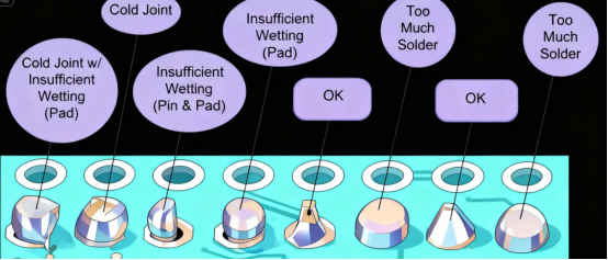
Common Causes of Poor Solder Fill and Solutions
In production, poor fill typically manifests in several ways:
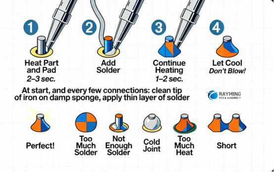
Poor Fill from Manual Soldering
Visual inspection often reveals solder joints that appear formed on the surface but lack solder inside the hole. Functional testing frequently confirms these as weak or “cold” joints.
This is common in manual soldering due to incorrect iron temperature and insufficient soldering time. The solution lies in optimizing manual soldering parameters, ensuring adequate temperature and contact time.
Excessive Connection of Hole Barrel to Internal Plane Layers
When a PTH connects to many internal copper planes, solder fill can be poor, leading to defective joints. This happens because the internal copper layers act as a heat sink, drawing heat away from the joint and preventing the solder from flowing fully.
The solution starts at the PCB design stage: using thermal relief pads instead of solid connections reduces heat dissipation, allowing the solder to stay molten longer and fill the hole.
Contamination or Oxidation Blocking Solder Flow
Oxides, oils, or other contaminants on the hole wall or component leads significantly reduce solder wettability, leading to poor fill. Holes must be properly processed to remove contaminants before the filling step to ensure optimal solder flow.
Solutions include stricter incoming quality control for PCBs and components, ensuring cleanliness, and optimizing flux application for coverage and volume. Additionally, optimizing the filling process can help prevent poor fill by ensuring that holes are adequately filled and prepared for subsequent soldering steps.
Practical Tips for Improving Solder Fill Quality
·Optimize Preheat Parameters: Sufficient preheating effectively removes moisture from the PCB and holes, reduces the chance of outgassing during soldering, and improves solder fluidity.
·Select the Appropriate Flux: Choose a flux with suitable activity and wetting properties based on the specific PCB and component characteristics.
·Strictly Control Soldering Temperature and Time: Ensure the solder has sufficient activity and fluidity, while avoiding excessively high temperatures that could damage components.
·Perform Regular Equipment Maintenance: Check wave solder equipment for wave stability, flux spray system performance, and overall process consistency.
·For High-Reliability Products: Where requirements for PCBA solder fill are stringent, consider using Selective Wave Soldering. This technology can significantly reduce instances of poor fill.
·Tip: Implementing automated assembly can further improve the consistency and quality of solder fill by minimizing manual errors and ensuring repeatable manufacturing processes.
Inspection Standards for Solder Fill Quality
According to IPC standards, solder fill requirements vary for different applications:
·Standard Through-Hole Joints: Typically require a fill rate greater than 75%.
·PTHs Connected to Heat Sink or Plane Layers: May have a reduced requirement, often greater than 50%.
·High-Reliability Products (e.g., military, aerospace): Often demand 100% solder fill, verified via cross-sectioning.
·Type VII via fill: For HDI boards and via-in-pad or stacked microvias, the Type VII standard specifies strict criteria for via fill quality, including proper adhesion and surface quality to ensure reliable assembly.
Inspection methods include cross-section analysis (microsection), X-ray inspection, and visual examination. Cross-sectioning is the most accurate method but is destructive. X-ray inspection provides a non-destructive means to assess fill quality.
Summary
Plated Through-Hole solder fill is a deceptively simple yet critically important step in the PCB assembly process. It encompasses knowledge from PCB design, material selection, and process parameter control. Only by deeply understanding the principles and influencing factors of solder fill can manufacturers effectively control its quality in production, thereby enhancing the reliability and longevity of electronic products.
As electronic devices continue trending towards "lighter, thinner, shorter, and smaller" with increasingly dense PCBs, the demands on solder fill processes become ever more stringent. Mastering the core technology of this process will be a key differentiator for electronics manufacturing companies seeking to enhance product quality and competitiveness.
We hope this detailed explanation provides a comprehensive understanding of Plated Through-Hole solder fill and empowers you to apply this knowledge in practical scenarios to troubleshoot issues and improve product quality.
FAQs
A. What is plated through-hole solder filling?
Q. It refers to the process during the soldering of PCB plated through-holes where solder fills the hole and wets the hole wall, aided by capillary action and other forces. The purpose is to ensure the electrical connection and mechanical fixation strength between the component and the through-hole.
A. What is the acceptable filling standard for this process?
Q. According to the IPC-A-610H standard, the target is 100% filling; the minimum acceptable filling percentage for Class 1-3 products is 75%, allowing for a maximum cumulative depression of 25% on the primary and secondary sides.
A. What are the key factors affecting the solder filling result?
Q. Mainly include hole wall cleanliness (residual oxides reduce filling effectiveness), the gap size between the through-hole and the component lead, the selection and application uniformity of flux, as well as process parameters like preheat temperature and soldering time during wave soldering.
A. What are the consequences of insufficient solder filling?
Q. It significantly reduces the mechanical strength of the solder joint, increases electrical resistance, not only impairing the PCB's conductivity but also weakening the solder joint's resistance to thermal fatigue, potentially leading to poor component contact or even complete failure in severe cases.
A. How to address issues like voids or blowholes during filling?
Q. Bake the PCB before soldering to remove moisture; increase preheat time or temperature; control the amount of flux used and ensure thorough volatilization before soldering; simultaneously, optimize PCB manufacturing processes to avoid rough hole walls and substrate porosity.
A. Are the filling requirements different for small-diameter and large-diameter plated through-holes?
Q. Yes, there is a difference. Typically, small-diameter through-holes require complete solder filling; large-diameter through-holes do not need to be completely filled, but the inner surface and top surface of the hole must be adequately wetted by the solder.
A. How to improve the solder filling quality of plated through-holes?
Q. Reduce the fit gap between the through-hole and the component lead to enhance capillary action; select compatible flux and apply it uniformly; control wave soldering time to 3-5 seconds, while matching with an appropriate soldering temperature.
Author: Jack Wang

