


Understanding PCB Coefficient of Thermal Expansion (CTE) and Its Effects
Every electronic device relies on the stability of its printed circuit board (PCB). When a PCB heats up or cools down, it slightly changes size—a property called thermal expansion. The measure of this change is the coefficient of thermal expansion (CTE), usually expressed in ppm/°C. Even small expansions or contractions can put stress on solder joints and components, potentially affecting performance and long-term reliability.
Because these thermal changes can impact board performance in subtle but important ways, designers need to understand how CTE works and how it interacts with materials, layer structures, and component placement. Grasping these concepts helps prevent common issues like solder joint cracking, board warping, or signal reliability problems.
So, how can engineers fully understand PCB CTE and apply this knowledge in real designs?
PCBMASTER, with years of experience as a leading PCB and PCBA supplier, will guide you through the key concepts. In the following sections, we will cover:
l What PCB CTE is
l How PCB CTE affects board performance
l Practical considerations for managing PCB thermal expansion
l How to measure and predict PCB CTE
l Why PCB CTE matters
What is the Coefficient of Thermal Expansion (CTE) in PCBs?
The Coefficient of Thermal Expansion (CTE) in PCBs is a measure of how much a printed circuit board expands or contracts when the temperature changes. It is critical for PCB reliability because differences in CTE between the board and electronic components can cause stress, warping, or solder joint failures.
Definition of CTE and Its Measurement Units
CTE is the ratio of a material’s change in size to its original size for each degree Celsius of temperature change.
CTE describes how much a PCB will grow or shrink when heated or cooled. It is measured in parts per million per degree Celsius (ppm/°C). For example, if a PCB has a CTE of 17 ppm/°C, it will expand 17 millionths of its original size for every 1°C increase in temperature.
Example: A 100 mm PCB with a CTE of 17 ppm/°C heated by 100°C expands by:
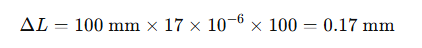
This simple calculation shows how even small CTE differences can impact solder joints and board reliability, especially for multi-layer boards or high-density designs.
How CTE Varies Across PCB Materials
Different PCB materials expand at different rates, and CTE can vary in different directions within the same board.
| PCB Material | Typical CTE (ppm/°C) |
|
| ||||
| FR-4 | 14–17 | X/Y (planar) | Most common PCB material; higher CTE in Z (thickness); general-purpose boards | ||||
| BT Resin | Slightly lower than FR-4 | X/Y | Used for fine-pitch PCBs; better dimensional stability than FR-4 | ||||
| Polyimide | Low | X/Y | Flexible PCBs; good thermal stability; low planar expansion | ||||
| Ceramic PCBs | Extremely low | X/Y and Z | High-temperature applications; RF boards; very low expansion | ||||
| Metal-Core PCBs | Moderate | X/Y and Z | High thermal conductivity; used for heat dissipation; moderate expansion |
Anisotropic Expansion: PCB CTE is rarely uniform. X/Y directions (along the plane) are usually smaller than Z direction (through the thickness). This difference is important when designing multi-layer boards to avoid warping or layer separation.
Factors Affecting PCB CTE
PCB CTE depends on multiple design and material factors, which engineers must consider to ensure reliability.
l Layer Count and Thickness: More layers or thicker boards generally reduce planar expansion but increase Z-direction stress.
l Copper Content and Distribution: Heavy copper areas reduce thermal expansion in-plane but can cause uneven warping if unbalanced.
l Resin Type and Filler Content: Epoxy or resin type and filler materials like silica can lower CTE. Higher filler content often reduces expansion.
l Temperature Range (Glass Transition, Tg): Above Tg, resin softens, and PCB expansion increases dramatically. Designers must consider operational temperatures to avoid thermal stress.
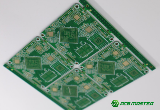
Real-Life Example: A 6-layer FR-4 PCB with uneven copper planes may bow slightly after a high-temperature solder reflow process due to CTE mismatch between copper and substrate, affecting solder joint reliability.
How Does PCB CTE Impact Solder Joint Reliability and Component Performance?
PCB CTE affects how much the board expands or contracts relative to the components mounted on it. When there is a mismatch between the PCB and component CTE, it creates thermal stress that can damage solder joints, cause board warpage, and affect sensitive electronics.
Thermal Stress on Solder Joints
Thermal stress occurs when the PCB and the IC/package expand at different rates during heating and cooling cycles.
Solder joints connect components like BGAs (Ball Grid Arrays) and QFNs (Quad Flat No-leads) to the PCB. If the PCB CTE is higher than the component’s CTE, the board expands faster, pulling on the solder joints during heating. When cooled, the board contracts, pushing the joints. Repeating this cycle creates fatigue stress, leading to cracks or joint failure.
Step-by-step Example of Thermal Cycling Stress:
1. PCB is heated to solder reflow temperature (~250°C).
2. PCB expands more than BGA component due to higher CTE.
3. Solder joints stretch, creating mechanical stress.
4. PCB cools; PCB contracts faster than component, causing compression stress.
5. After multiple cycles, solder joints may crack or lift.
Practical Note: Using a low-CTE PCB material or matching the component CTE can significantly reduce thermal stress.
Board Warpage and Layer Separation
Differences in expansion in the Z-direction (through thickness) can cause PCB warpage or layer separation, especially in multi-layer boards.
When a PCB heats up, each layer expands differently because of material differences. Uneven expansion causes the board to warp or bend, leading to misaligned components or mechanical stress. In extreme cases, the layers inside a multi-layer PCB can delaminate, reducing board reliability.
Visual Example:
l Flat PCB: Uniform expansion, all layers remain bonded.
l Warped PCB: Center or edges bend, creating gaps between layers and stressing solder joints.
PCBMASTER engineers mitigate this by carefully balancing copper distribution and selecting materials with compatible CTE in all layers.
Effect on High-Speed and Sensitive Electronics
Micro-movements from PCB CTE can disrupt high-speed signals and affect sensitive electronics.
In high-frequency PCBs, even tiny shifts due to thermal expansion can cause signal integrity problems, like timing delays, crosstalk, or impedance mismatch. Flexible PCBs and fine-pitch ICs are particularly sensitive because small mechanical changes affect electrical performance.
Case Study:
l A 5-layer RF board with uneven copper planes experienced intermittent signal errors after repeated thermal cycles.
l Engineers replaced part of the board with low-CTE laminate and optimized stack-up. Signal integrity improved, showing the direct impact of CTE control on performance.
Practical Advice: For high-speed or sensitive designs, always consider PCB CTE when selecting materials and designing the layout.
What Are the Best Practices to Control PCB Thermal Expansion (CTE)?
Controlling PCB CTE is essential to prevent solder joint failures, warpage, and signal issues. Best practices include selecting suitable materials, designing balanced PCB stack-ups, and following careful manufacturing and assembly procedures.
Material Selection Strategies
Choosing the right PCB material is the first step to control CTE and ensure board reliability.
Low-CTE laminates, such as BT resin, polyimide, or specialized FR-4 with fillers, reduce thermal expansion. These materials help align the PCB’s CTE with the components, decreasing solder joint stress during temperature changes.
Trade-offs: Low-CTE materials typically cost more than standard FR-4. Designers must balance budget vs. performance. For example, in high-density BGA designs, using a low-CTE BT resin laminate reduces solder fatigue but increases material cost by 20–30%. PCBMASTER recommends analyzing component sensitivity, operating temperature, and reliability requirements before choosing the material.
PCB Stack-Up Design Considerations
A well-designed PCB stack-up helps minimize warpage and thermal stress caused by CTE mismatch.
l Symmetrical Layer Design: Ensuring the PCB stack-up is symmetrical (equal copper and dielectric layers above and below the central plane) reduces bending and warping during heating.
l Copper Plane Placement: Proper placement of copper planes balances thermal expansion. Uneven copper distribution causes differential expansion, leading to stress and board bow. For example, a 6-layer board with heavy copper only on one side may warp by 0.2 mm after solder reflow, whereas a balanced design remains flat.
PCBMASTER provides guidance on stack-up design to optimize thermal and mechanical stability for different CTE requirements.
Manufacturing and Assembly Tips
Certain manufacturing and assembly practices can reduce CTE-related issues and improve PCB reliability.
Pre-Baking Boards: Moisture in the PCB can expand during reflow, increasing stress. Pre-baking removes moisture, preventing unexpected expansion.
Optimized Soldering Profiles: Controlling heating and cooling rates during reflow minimizes thermal stress on solder joints and prevents warpage. Step-by-step:
1. Ramp up to reflow temperature slowly.
2. Maintain peak temperature for sufficient solder melting.
3. Cool down gradually to reduce contraction stress.
Practical Example: A PCBMASTER multi-layer board for a high-frequency application maintained flatness after thermal cycling by combining low-CTE material, balanced stack-up, and a controlled soldering profile.
How Can Engineers Measure and Predict PCB CTE?
Engineers measure and predict PCB CTE using a combination of experimental methods, simulation tools, and reliable manufacturer data. Accurate CTE information helps prevent solder joint failures, warpage, and signal integrity issues in PCBs.
Experimental Methods for CTE Measurement
Experimental methods allow engineers to directly measure how much a PCB expands when heated.
Thermomechanical Analysis (TMA): TMA measures dimensional changes of a PCB sample as it is heated. The device applies a small force and records expansion, providing CTE values in X, Y, and Z directions.
Dilatometry: Dilatometry also measures expansion, typically by tracking length changes of a sample inside a furnace with high precision. This method is common for comparing materials before board fabrication.
Lab Setup Example: A simple lab test includes mounting a PCB sample in a TMA machine, heating from room temperature to 150°C, and recording expansion curves. Engineers can then calculate the average CTE and check for anisotropic behavior.
These methods provide real, measured CTE values, which are essential for validating simulation models and material specifications.
Simulation Tools and Predictive Modeling
Simulation tools help predict PCB CTE behavior before manufacturing, saving time and cost.
Finite Element Analysis (FEA): FEA simulates thermal expansion and mechanical stress in multi-layer PCBs. Engineers input material CTE, copper distribution, and layer stack-up to predict warpage and solder joint stress under thermal cycling.
Software Recommendations: Common tools include ANSYS, COMSOL, and Altium Designer for PCB thermal analysis. These programs allow engineers to model expansion, identify high-stress areas, and optimize the board design for CTE compatibility.
Practical Use: Engineers can simulate a BGA-mounted PCB and see how thermal cycles affect solder joints. They can adjust the material or copper plane placement in the model before fabrication, reducing trial-and-error costs.
Using PCBMASTER Data for Accurate Design
PCBMASTER provides verified CTE and material specifications to support accurate design and simulation.
All PCB materials supplied by PCBMASTER come with detailed datasheets, including X/Y and Z-direction CTE values, glass transition temperature (Tg), and thermal conductivity. Designers can use this data to select the right laminate, optimize stack-up, and feed accurate numbers into simulations.
Example: When designing a high-density BGA board, engineers reference PCBMASTER’s FR-4 low-CTE material data to match the component CTE. Using accurate CTE values ensures solder joint reliability and prevents board warpage during thermal cycling.
This approach combines empirical data, simulation, and design best practices to produce reliable, high-performance PCBs.
Why Does PCB CTE Matter in Modern Electronics?
PCB CTE is critical in modern electronics because mismatches in thermal expansion can reduce reliability, damage solder joints, and impact high-density, miniaturized designs. Controlling CTE ensures performance, longevity, and compliance with industry standards.
Reliability in Consumer vs Industrial Electronics
PCB CTE affects product lifespan and reliability differently in consumer and industrial applications.
Consumer Electronics: Devices like smartphones and tablets often use standard FR-4 boards with minimal CTE control. Mismatches between the PCB and component CTE can cause micro-cracks in solder joints, leading to shorter lifespans and early failures after repeated thermal cycling.
Industrial and Aerospace Electronics: These applications require PCBs with strictly controlled low-CTE materials to ensure reliability under extreme temperatures and mechanical stress. For example, aerospace PCBs use BT resin or ceramic materials to minimize expansion and prevent solder joint fatigue, ensuring stable operation over decades.
Practical Insight: Selecting appropriate materials for the application type is essential. PCBMASTER provides a range of low-CTE laminates suitable for both consumer and industrial boards.
Impact on Miniaturized and High-Density PCBs
Miniaturized and high-density PCBs are extremely sensitive to CTE-induced stress.
Components like BGAs (Ball Grid Arrays) and CSPs (Chip-Scale Packages) have small solder balls that can crack if the PCB expands or contracts unevenly. This is especially critical in mobile phones, which have compact, dense PCBs, versus server motherboards, which are larger and can tolerate slight expansion better.
Example: A smartphone PCB with mismatched CTE may develop micro-cracks in BGA solder joints after a few thermal cycles, causing intermittent failures. In contrast, a server motherboard with larger, less dense components may not show immediate failure under the same thermal stress.
Practical Tip: For high-density, miniaturized designs, use low-CTE laminates and consider balanced stack-ups to reduce solder joint fatigue.
Regulatory and Quality Considerations
Industry standards set limits on PCB thermal expansion to ensure quality and reliability.
IPC Standards: IPC-2221 and IPC-6012 provide guidelines for allowable PCB thermal expansion and material selection. These standards help designers prevent warpage, delamination, and solder failures.
Compliance Importance: PCBA manufacturers must follow these limits to guarantee product safety, avoid warranty claims, and meet customer requirements. For example, failure to meet IPC standards can result in non-compliant aerospace or medical electronics, where thermal reliability is critical.
Practical Insight: Using verified PCBMASTER materials and documented CTE specifications helps engineers design boards that meet IPC standards and ensures long-term reliability.
Conclusion – PCBMASTER’s Approach to Optimizing CTE for Reliable PCBs
Understanding PCB Coefficient of Thermal Expansion (CTE) is essential for designing reliable electronics. Mismatched CTE between a PCB and its components can lead to solder joint failures, board warpage, and signal integrity issues. By carefully selecting materials, optimizing stack-up design, and controlling manufacturing processes, engineers can significantly reduce thermal stress and extend product longevity.
To navigate these challenges effectively, many designers rely on partners who offer both high-quality materials and practical design guidance. PCBMASTER provides extensive expertise in low-CTE laminates, detailed material datasheets, and professional support for stack-up optimization and thermal management. Leveraging these resources helps engineers design PCBs that maintain reliability even under demanding thermal cycles.
By taking advantage of PCBMASTER’s materials and technical guidance, engineers can optimize their PCB designs for thermal stability, improve solder joint longevity, and meet rigorous industry standards. This collaborative approach ensures that modern, high-density, and high-performance electronics perform reliably throughout their lifecycle.
FAQ – Common Questions About PCB CTE
What is a typical CTE value for standard FR-4 PCB materials?
A standard FR-4 PCB usually has a CTE of 14–17 ppm/°C in the X/Y (planar) directions and a higher CTE in the Z (thickness) direction. This means the board expands 14–17 millionths of its size per degree Celsius along the plane, while expansion through the thickness can be greater.
Can mismatched CTE between PCB and components cause early failures?
Yes. When the PCB and mounted components, like BGAs or QFNs, have different CTEs, thermal cycling creates stress on solder joints. Over time, this stress can lead to micro-cracks or solder joint failure, reducing product reliability and lifespan.
How can designers reduce warpage in multi-layer PCBs?
Designers can reduce warpage by creating a symmetrical stack-up, balancing the number of copper and dielectric layers above and below the central plane. Proper placement of copper planes also helps distribute thermal expansion evenly, minimizing bending or delamination.
Does temperature cycling accelerate solder joint fatigue?
Yes. Repeated heating and cooling causes the PCB and components to expand and contract at different rates. This thermal cycling accelerates solder fatigue, which can eventually lead to cracks or lift-offs in solder joints.
Can PCBMASTER provide custom PCB materials with specific CTE ranges?
Yes. PCBMASTER offers a variety of low-CTE laminates and can provide technical guidance for stack-ups and material selection. This ensures designers can achieve CTE-optimized PCBs that meet reliability requirements for high-density, industrial, or aerospace applications.

