PTFE PCB The Performance Champion in the High-Frequency Electronics Field
In today’s era of rapid electronic device iteration, printed circuit boards (PCBs) serve as the “hardware nervous system,” directly determining the signal transmission efficiency and stability of devices. In high-frequency and extreme environment scenarios, PTFE PCBs (also known as Teflon PCBs or Teflon circuit boards) stand out with their unique performance, becoming an “essential material” in high-end fields such as 5G communications and aerospace, especially for advanced communication systems. Today, we will break down this “specialized PCB” in plain language to understand why it has become a “hot commodity” in the high-frequency field.
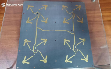
PTFE PCBs are engineered for demanding environments. This type of printed circuit board is specifically designed for high-frequency and advanced communication applications.
First, Understand: What Exactly is a PTFE PCB?

·PTFE, short for Polytetrafluoroethylene, is more commonly known by its trade name “Teflon”—the high-temperature resistant, non-stick coating material used on the surface of non-stick pans. PTFE is a synthetic fluoropolymer, valued for its non-reactive nature and low dielectric constant. PTFE-based materials are widely used in high-frequency PCB manufacturing due to their excellent electrical, thermal, and mechanical properties. A PTFE PCB is a circuit board made with PTFE as the base material. Compared to the common FR-4 PCBs (ordinary circuit boards), it is like a “special forces unit,” specifically designed to handle high-frequency, high-temperature, and strong corrosion scenarios that ordinary PCBs cannot withstand. PTFE-based material can be engineered with various fillers and reinforcements to tailor its properties for specific applications.
·To put it simply: Ordinary FR-4 PCBs are suitable for daily devices such as mobile phone chargers and routers, while PTFE PCBs serve high-end devices with “stringent performance requirements” like 5G base stations, satellite communications, and automotive radar. These are often PTFE-based composites, designed to meet demanding electrical and mechanical standards.
"Hardcore Advantages" of PTFE PCBs That Ordinary PCBs Cannot Match

"Zero Distortion" and Low Dielectric Constant for High-Frequency Signals: The "Signal Bodyguard" for Communication Devices
What do high-frequency electronic devices fear the most? “Problems” during signal transmission—either excessive loss or waveform distortion. However, PTFE has an extremely stable molecular structure, which gives it two key performance features:
·Ultra-low dielectric constant (Dk ≈ 2.0-2.2): This is equivalent to signals transmitting on a “smooth highway,” with stable phase and no “deviation” caused by material interference; it also provides very low dielectric losses and high frequency performance, making PTFE ideal for demanding RF and microwave applications.
·Ultra-low dissipation factor (Df ≈ 0.0005-0.002): The “energy loss” during signal transmission is more than 80% lower than that of FR-4. For example, in the 28GHz frequency band of 5G, PTFE PCBs allow signals to “travel farther and more clearly.” This minimal dissipation factor ensures low energy dissipation, which is critical for maintaining signal integrity in high-frequency environments.
·Take an example: The AAU antenna module of a 5G base station uses PTFE PCBs to reduce signal insertion loss, making the 5G signal received by mobile phones more stable; satellite communications also rely on PTFE PCBs to ensure uninterrupted “space-ground communication” when transmitting Ka-band signals in space. PTFE PCBs are also ideal for high speed digital circuits, RF applications, and microwave and RF applications due to their superior frequency characteristics and ability to meet systems that require superior frequency.
·These advantages make PTFE the material of choice for high frequency pcbs and rf pcb in advanced communication and aerospace systems.
2. Withstands Extreme Temperatures: Unaffected by Extreme Cold or High Heat
·Ordinary FR-4 PCBs will deform at temperatures above 130°C, while PTFE PCBs have an operating temperature range from -200°C (close to the low temperature of the Antarctic) to 260°C (comparable to the high temperature of an oven). Within this range, their electrical performance barely drifts. PTFE PCBs also offer excellent thermal stability and higher thermal conductivity, which contribute to their reliability and effective thermal management in extreme environments.
·This feature is particularly important in the aerospace and automotive fields: The temperature of electronic devices near aircraft engines often exceeds 150°C; the temperature of automotive radar circuit boards also soars after exposure to intense summer sunlight. PTFE PCBs can remain “stable as a mountain” in these environments and will not cause equipment failure due to temperature fluctuations.
3. Resistant to Chemical Corrosion: The "Durability King" in Harsh Environments
·PTFE is a well-known “chemically inert material”—it is not damaged by strong acids, strong alkalis, or organic solvents, and its water absorption rate is less than 0.01% (almost non-absorbent). Its excellent chemical resistance makes it highly suitable for use in corrosive chemical environments where other materials would degrade.
·For example, sensors in chemical workshops are exposed to corrosive gases all year round. Ordinary PCBs will be corroded and short-circuited within a few months, while PTFE PCBs can work stably for a long time; outdoor 5G base stations will not experience signal distortion due to water absorption even in heavy rain or high-humidity weather.
·The intrinsic properties of PTFE PCBs remain unaltered even when exposed to harsh chemicals, extreme temperatures, or moisture, ensuring durability and stability under challenging conditions.
4. Reliable Mechanical Performance: Resistant to Vibration and Friction
·Although PTFE itself is relatively soft, adding ceramic powders (such as SiO₂) can significantly improve its mechanical strength and dimensional stability. Ceramic fillers not only enhance the mechanical rigidity of PTFE laminates but also improve their thermal and electromagnetic properties, making them ideal for high-frequency applications. Compared to glass reinforcement or glass fiber, which provide high mechanical rigidity and structural stability, ceramic fillers offer superior phase response and dielectric performance at RF frequencies. However, glass fiber and glass reinforcement can introduce weave effects and phase response issues at high frequencies. Unreinforced material, which contains no additional reinforcement like woven glass fibers or ceramic fillers, is much more flexible but can be challenging to handle and manufacture due to its lack of rigidity. Moreover, it has an extremely low friction coefficient, making it suitable for devices that require frequent vibration—such as the flight control circuit boards of drones. In high-altitude vibration environments, PTFE PCBs can reduce component wear and extend the service life of equipment.
How Are PTFE PCBs Manufactured? 3 Key Process Challenges and Breakthroughs

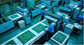
PTFE has “outstanding advantages,” but it is much more difficult to manufacture than ordinary FR-4. The core lies in solving 3 problems. In Teflon PCB manufacturing, the key manufacturing steps involved include specialized surface preparation, copper plating, drilling, and lamination, all of which require precise control and expertise. These complex processes are typically handled by experienced PCB fabricators who specialize in high-frequency and advanced material circuit boards.
1. Ensuring PTFE and Copper Foil "Adhere Firmly"
The surface of PTFE is too smooth and inert, so copper foil easily peels off if directly attached. The current mainstream solution is “surface activation treatment”:
·Etching the PTFE surface with plasma to increase roughness and introduce “adhesive groups”;
·Or treating it with a sodium-naphthalene solution to form tiny pits on the surface, then performing high-temperature lamination (300-400°C, 20-40MPa pressure) with copper foil to ensure firm bonding.
·After surface activation, careful copper plating is essential to ensure reliable adhesion of copper to the PTFE substrate and to prevent defects such as pad lifts or barrel cracks. It is also important to prevent surface oxidation during storage and handling, as oxidation can degrade surface quality and negatively impact copper adhesion.
·After surface preparation and lamination, copper plating is a critical step to create robust electrical connections and enhance the durability of the PCB.
2. Precision Drilling: Avoiding "Burrs" and Deformation
PTFE is relatively soft, so traditional mechanical drilling tends to cause burrs and deformation on the hole walls. Because of these challenges, manufacturers often favor ceramic filled laminates for their ease of drilling, improved structural integrity, and reliable via formation, especially in high-precision manufacturing processes.
Two methods are now used instead:
·Using diamond-coated drills for low-speed drilling (30-50m/min) and matching with cooling fluid to reduce heat generation; ceramic filled laminates are advantageous here, as they facilitate easier drilling and maintain better hole quality.
·Using laser drilling directly for microholes (diameter < 0.15mm), which achieves higher precision and avoids mechanical stress.
3. Multilayer Board Lamination: Preventing "Delamination and Warping"
·PTFE has a high coefficient of thermal expansion, so multilayer boards are prone to delamination due to inconsistent expansion of each layer during lamination. Selecting the right laminate material and PTFE laminates is crucial for achieving dimensional stability in these multilayer structures. PTFE laminate materials, especially those with ceramic or glass reinforcements within the PTFE matrix, significantly enhance the performance and reliability of multilayer boards by improving structural integrity, flame resistance, and bonding capabilities.
The solution is “stepwise heating + low pressure”:
·First preheating to 150-200°C to release stress;
·Then heating in stages (90°C → 150°C → 200°C) and laminating at a low pressure of 100-200psi to allow each layer to “expand synchronously” and ensure dimensional stability. The use of PTFE laminate in this process is essential for proper bonding and maintaining the desired properties of the multilayer assembly.
Where Are PTFE PCBs Used? 4 Core Application Scenarios
Currently, PTFE PCBs mainly serve “high-end essential fields,” with 4 common application scenarios. When comparing various PCB materials, PTFE stands out due to its unique material properties, such as excellent dielectric performance and high heat resistance, making it ideal for advanced electronic and communication systems. The selection of PCB materials depends on the specific application requirements, with PTFE often chosen for its superior electrical and thermal characteristics. Commercial Teflon PCBs are widely used in industrial and commercial applications, including wireless communication devices and active safety systems, due to their cost-effectiveness and reliable high-frequency performance.
1. 5G/6G Communications: The "Signal Core" of Base Stations and Satellites
·The AAU antennas and Massive MIMO systems of 5G base stations rely on PTFE PCBs to reduce high-frequency signal loss; PTFE PCBs are especially important for transmitting signals at higher frequencies, and Rogers PCBs are widely used in these applications due to their superior frequency performance and suitability for advanced RF and microwave systems.
·The phased array antennas of low-Earth orbit (LEO) satellites use PTFE PCBs to achieve “ultra-low loss transmission” of Ka-band signals, and future 6G terahertz communications will also be inseparable from them.
2. Automotive Electronics: The "Eye Protection" for Autonomous Driving
·77GHz automotive radar is the “eye” of autonomous driving, with extremely high requirements for signal accuracy. PTFE PCBs ensure that the radar can accurately detect surrounding vehicles and pedestrians; common teflon pcbs and commonly used teflon pcbs, such as Rogers and RT series, are widely applied in these automotive radar systems for their reliable high-frequency performance. Teflon boards play a crucial role in automotive electronics by providing stable signal transmission and durability in harsh environments.
·The 800V high-voltage on-board charger (OBC) of new energy vehicles uses the high-temperature resistance and low-loss characteristics of PTFE PCBs to increase charging efficiency to over 96%.
3. Aerospace: The "Reliable Choice" for Extreme Environments
·Aircraft navigation systems and missile control modules rely on PTFE PCBs to ensure uninterrupted signals amid temperature fluctuations from -55°C to 200°C; military-grade Teflon PCBs, such as those using Rogers RT5000 and RT600 series, are specifically engineered for aerospace and defense applications where superior thermal stability, signal integrity, and durability are required;
The electronic equipment of space probes also relies on PTFE PCBs to maintain stable operation in the face of space radiation and extreme temperature differences.
4. Medical Equipment: The "Auxiliary Expert" for Precise Diagnosis
·Magnetic Resonance Imaging (MRI) equipment requires high-precision signal transmission. PTFE PCBs can reduce signal interference and make medical images clearer;
·Some implantable devices (such as pacemakers) are also being tested with PTFE PCBs, utilizing their biocompatibility and stability to reduce the risk of human rejection.
·Teflon PCB orders for medical equipment often require customization and rapid fulfillment to meet strict regulatory and performance standards.
How to Choose a PTFE PCB? 4 Key Points

For engineers or purchasers, choosing the right PTFE PCB does not require “blindly pursuing high-end products.” It is important to select reputable teflon pcb manufacturers, as their market presence, product offerings, and quality can significantly impact your project. Additionally, considering cost efficiency is crucial when evaluating different PTFE PCB options to ensure you receive optimal value without unnecessary expenses. The key lies in 4 aspects:
1. First, Clarify "Core Requirements"
·High-frequency communications (e.g., 5G base stations): Prioritize products with Dk = 2.0-2.2 and Df < 0.0015; the electrical characteristics, such as low dielectric loss, consistent dielectric constant across frequencies, high volume resistivity, and high breakdown voltage, are crucial for optimal performance in these applications.
·Extreme temperatures (e.g., automotive radar): Choose products with an operating temperature range of -55°C to 260°C and a coefficient of thermal expansion (CTE) < 12ppm/°C;
·Corrosive environments (e.g., chemical sensors): Confirm that the water absorption rate is < 0.01% and that the product can withstand the corresponding chemical substances.
2. Evaluate the Manufacturer’s "Technical Strength"
The manufacturing threshold of PTFE PCBs is high. Prioritize manufacturers with the following capabilities:
·An independent R&D team for material formulas, capable of customizing products to meet special needs;
·Specialized equipment such as laser drilling and high-temperature lamination machines;
·Certifications such as ISO 9001, IATF 16949 (automotive industry), and AS9100 (aerospace industry). When evaluating teflon pcb manufacturers, request test reports to verify product quality.
3. Balance "Cost and Performance"
PTFE PCBs are 5-8 times more expensive than FR-4, but costs can be controlled through 3 methods while ensuring performance:
·Non-extreme scenarios: Choose PTFE composite materials filled with glass fibers to reduce costs by 20%-30%;
·Bulk procurement: Sign long-term agreements with manufacturers to enjoy a 10%-15% discount on bulk orders;
·Simplify design: Reduce unnecessary blind holes and microholes to lower process difficulty.
4. Pay Attention to "After-Sales Service and Support"
Prioritize manufacturers that can provide the following services:
·Design consultation: Assist in optimizing PCB layout and heat dissipation design;
·Test reports: Provide test data on dielectric properties, thermal stability, etc.;
·On-site support: Offer on-site assistance to solve problems when they occur, which is particularly important for high-end equipment.
Future Trends: Will PTFE PCBs Become "Stronger" and "Cheaper"?
The answer is yes. Currently, there are 3 obvious trends in the industry:
1. Better Performance: Moving Toward "Ultra-High Frequencies"
Researchers are developing PTFE materials with Dk < 2.0 and Df < 0.0005 to meet the needs of future 6G terahertz (above 100GHz) communications and further reduce signal transmission loss.
2. Lower Costs: Large-Scale Production + Process Simplification
Leading manufacturers are expanding production capacity (e.g., increasing monthly capacity from 5,000㎡ to 20,000㎡), reducing unit costs by more than 25%;
Integrated equipment (such as "plasma etching + cleaning" all-in-one machines) shortens process time and further reduces costs.
3. Wider Applications: From "High-End" to "Consumer-Grade"
As costs decrease, PTFE PCBs are beginning to enter consumer electronics: for example, the millimeter-wave antennas of high-end 5G mobile phones and the signal modules of VR devices. In the future, they may also be used in smart wearable devices to improve high-frequency signal stability.
Conclusion
PTFE PCBs are not "universal PCBs," but in high-frequency and extreme environments, they are irreplaceable "performance champions." From 5G base stations to satellites, from autonomous driving cars to medical equipment, they silently ensure the stable operation of high-end electronic devices.
In the future, with the development of 6G, space exploration, and autonomous driving, PTFE PCBs will become "stronger" and "cheaper," with even wider application scenarios. For enterprises and engineers, understanding the performance advantages of PTFE PCBs and choosing the right products will help seize opportunities in the development of the high-end electronics industry.
Why choose PCBMASTER: https://www.pcbmaster.com/why
Join us: https://www.pcbmaster.com/login

