


PCB Depanelization Methods: How to Remove Breakaway Tabs Safely and Efficiently
PCB depanelization is the process of separating individual circuit boards from a manufacturing panel after PCB fabrication or PCBA assembly. Choosing the right depanelization method directly affects product quality, reliability, assembly yield, and production efficiency. Common methods include V-Cut depanelization, CNC routing, punch depanelization, laser depanelization, and manual tab removal . Each technique has its own advantages, limitations, and suitable applications. For high-reliability electronics, controlling mechanical stress, dust contamination, ESD risks, and edge quality is critical. As a professional PCB and PCBA manufacturer, PCBMASTER helps customers select the most appropriate depanelization solution based on product design, production volume, and reliability requirements.
Why PCB Depanelization Matters
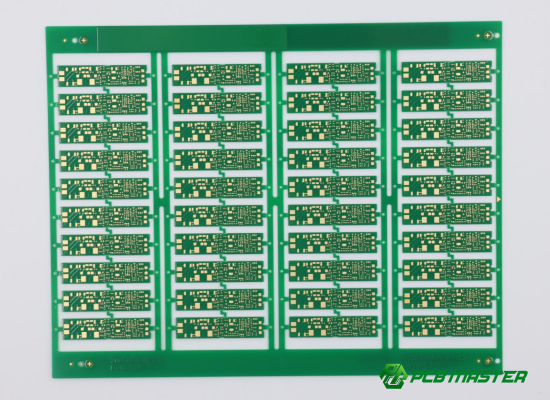
During PCB manufacturing, multiple boards are typically produced together on a larger panel to improve fabrication efficiency and reduce costs. Once assembly is completed, the individual PCBs must be separated without damaging components, solder joints, or circuit traces.
Improper depanelization can lead to:
- Cracked solder joints
- PCB delamination
- Broken components
- Hidden micro-cracks
- Edge burrs affecting assembly
- ESD-related failures
- Long-term reliability issues
Selecting the correct depanelization method is therefore an essential part of PCB and PCBA production.
Common PCB Depanelization Methods
V-Cut Depanelization
V-Cut (V-Scoring) is one of the most widely used PCB separation methods. During PCB fabrication, V-shaped grooves are pre-cut along the separation lines. A depaneling machine then applies controlled pressure to split the boards apart.
Advantages
- Low manufacturing cost
- Fast processing speed
- Suitable for mass production
- Simple panel design
Limitations
- Only suitable for straight-line board edges
- Rougher board edges after separation
- Generates mechanical stress during depanelization
- Not ideal for sensitive components near the scoring line
Best Applications
- Consumer electronics
- LED products
- Standard rectangular PCBs
CNC Routing (Milling Depanelization)
CNC routing uses a high-speed rotating milling cutter to cut along the PCB outline.
Advantages
- Extremely high precision
- Supports circular and irregular PCB shapes
- Cleaner board edges
- Lower mechanical stress compared with V-Cut
Limitations
- Higher equipment costs
- Generates dust and debris
- Longer processing time
Best Applications
- Industrial control systems
- Medical electronics
- Automotive electronics
- Complex-shaped PCBs
Punch Depanelization
Punch depanelization uses custom tooling and a press machine to separate PCBs in a single operation.
Advantages
- Extremely fast production speed
- Ideal for high-volume manufacturing
- Consistent separation quality
Limitations
- High tooling costs
- Limited flexibility for design changes
- High instantaneous mechanical impact
- Potential risk to fragile components
Best Applications
- Stable, high-volume products
- Consumer electronics production lines
Laser Depanelization
Laser depanelization removes material using a focused laser beam without physical contact.
Advantages
- No mechanical stress
- Extremely narrow cutting width
- Excellent precision
- Suitable for thin and flexible materials
Limitations
- High equipment investment
- Potential carbonization on cut surfaces
- Heat may affect temperature-sensitive components
- Slower for thicker boards
Best Applications
- Flexible PCBs (FPC)
- Rigid-flex PCBs
- Wearable electronics
- Miniaturized devices
Manual Depanelization (Tab Breaking)
Manual separation is typically performed on PCBs connected through breakaway tabs or mouse bites.
Advantages
- Minimal equipment investment
- Suitable for prototypes and small batches
Limitations
- High risk of board damage
- Inconsistent results
- Generates significant mechanical stress
- Not recommended for assembled PCBs
Best Applications
- Engineering samples
- Low-volume prototyping only
Comparison of PCB Depanelization Methods
Method Comparison Table
| Criteria | V-Cut | CNC Routing | Punching | Laser | Manual |
| Cost | Low | Medium-High | High Tooling Cost | High | Very Low |
| Precision | Medium | High | High | Very High | Low |
| Mechanical Stress | High | Low | High | None | Very High |
| Suitable for Irregular Shapes | No | Yes | Limited | Yes | Limited |
| Production Speed | Very Fast | Medium | Very Fast | Medium | Slow |
| Edge Quality | Fair | Excellent | Good | Excellent | Poor |
| Recommended for Sensitive Components | No | Yes | No | Yes | No |
PCBMASTER Best Practice
| Requirement | Standard Industry Approach | PCBMASTER Recommended Solution |
| High-Reliability Electronics | V-Cut or Manual Separation | CNC Routing or Laser Depanelization |
| Flexible PCB Processing | Mechanical Cutting | Laser Depanelization |
| Prototype Orders | Manual Separation | Precision CNC Routing |
| Automotive Electronics | Standard Depanelization | Low-Stress Routing with IATF 16949 Quality Control |
| Complex Board Shapes | Limited Processing Options | Advanced CNC Routing Capability |
Critical Considerations During PCB Depanelization
Mechanical Stress Control
Mechanical stress is the most significant risk during depanelization.
V-Cut and punch separation can create torsional forces that may cause:
- Solder joint cracks
- Component damage
- PCB delamination
- Hidden reliability failures
Best Practice
- Keep sensitive components at least 10 mm away from depanelization lines.
- Place fragile components parallel to the separation edge whenever possible.
- Use CNC routing or laser depanelization for high-reliability products.
Dust and Cleanliness
Routing and V-Cut processes generate fiberglass and resin dust.
If contamination remains on the PCB surface, moisture can create conductive paths that may lead to:
- Leakage current
- Signal integrity issues
- Short circuits
Best Practice
- Use industrial vacuum extraction systems.
- Add cleaning processes when required.
- Inspect boards after depanelization.
Edge Burrs and Dimensional Accuracy
Poor edge quality can interfere with:
- Connector insertion
- Enclosure assembly
- Mechanical fit requirements
Applications using edge connectors or gold fingers often require smoother board edges and tighter dimensional tolerances.
Best Practice
- Use CNC routing for precision assemblies.
- Perform secondary deburring if necessary.
ESD Protection
High-speed friction during depanelization can generate electrostatic discharge (ESD) .
ESD events may damage:
- ICs
- Sensors
- Communication modules
- Memory devices
Best Practice
- Use ESD-safe depanelization equipment.
- Install anti-static dust collection systems.
- Follow ESD-controlled manufacturing procedures.
Board Support and Fixturing
Insufficient support during depanelization can result in:
- PCB bending
- Trace cracking
- Solder joint failure
Best Practice
- Ensure full bottom-side support.
- Use dedicated fixtures for complex assemblies.
- Verify board flatness after separation.
PCBMASTER's Approach to Professional PCB Depanelization
As a leading PCB and PCBA manufacturing partner, PCBMASTER integrates depanelization planning into the entire production process rather than treating it as a final operation.
Leveraging an 80,000㎡ manufacturing facility , advanced production equipment, and a team of more than 50 professional engineers, PCBMASTER provides comprehensive support for:
- PCB fabrication
- SMT assembly
- PCBA manufacturing
- Design for Manufacturability (DFM)
- Depanelization optimization
Key Advantages
- IATF 16949, ISO 9001, UL, and RoHS certified manufacturing
- Free engineering file review before production
- Advanced AOI inspection and three-stage quality inspection
- 99.5% product yield rate
- 99.59% on-time delivery performance
- Support for HDI, High-Frequency, Rigid-Flex, FPC, and Metal Core PCBs
- 24-hour prototype services for urgent projects
By evaluating panel layouts, component placement, and end-use requirements early in the design phase, PCBMASTER helps customers minimize depanelization risks and improve overall product reliability.
Future Trends in PCB Depanelization
As electronics continue to become smaller, thinner, and more complex, depanelization technology is evolving toward:
- Higher precision laser processing
- Increased automation
- AI-assisted manufacturing optimization
- Lower-stress separation methods
- Enhanced quality monitoring systems
For advanced applications such as automotive electronics, medical devices, industrial automation, aerospace systems, and wearable technology, selecting the appropriate depanelization method is becoming increasingly important for ensuring long-term product reliability.
Choosing the right depanelization strategy is not simply about separating boards—it is a critical step in protecting product performance, manufacturing yield, and customer satisfaction.
Tags: #PCB #PCBA #SMT #PCBDepanelization #VCutPCB #CNCRouting #LaserDepanelization #RigidFlexPCB #FPC #PCBMASTER #ElectronicsManufacturing #PCBAssembly #DFM #AutomotiveElectronics #IndustrialControl #IndustryInsights
About the Author

Carol Luo
PCB Design EngineerI'm Carol, a PCB Engineer at PCBMASTER with experience in PCB design and manufacturing engineering since 2018. I focus on translating engineering requirements into reliable PCB solutions, with expertise in stack-up design, material selection, and design-for-manufacturing (DFM). I share practical engineering insights from real-world PCB design and production experience.
Visit Carol Luo's Profile

