


A Complete Guide to DIP (Dual Inline Package): Features, Applications, and Benefits
In an era where technology seems to evolve every day, some designs endure, quietly proving their worth in ways newer innovations can’t always match. The Dual Inline Package (DIP), first introduced in the 1970s, is one of those enduring classics. While surface-mount components dominate the modern landscape, DIP continues to play a crucial role in everything from educational kits to industrial machinery. Its simple, yet reliable design has made it a go-to choice for prototyping, repair, and even legacy systems that still rely on its ruggedness and ease of use. But what is it about DIP that keeps it relevant, even as the world moves towards smaller, faster solutions? Let’s explore how this timeless package has managed to hold its ground in a fast-moving tech world.
Introduction to Dual Inline Package (DIP)
What is DIP?
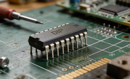
The Dual Inline Package (DIP) is a type of electronic component used in circuit boards. It’s a through-hole package, meaning the component has two rows of metal pins that go through holes on a printed circuit board (PCB) for soldering. These pins are typically spaced 0.1 inches apart, which makes them easy to work with when creating or repairing electronic circuits.
Think of a DIP as a rectangular block with metal legs on each side. Each leg, or pin, connects to the circuit board, allowing the electronic component inside to communicate with other parts of the circuit. Commonly used components inside a DIP package include microcontrollers, memory chips, and transistors.
DIP components were first introduced in the 1970s and became widely used because they were simple to handle, especially in the days before more modern technologies like Surface-Mount Technology (SMT). Despite the rise of smaller, more compact designs, DIP components are still popular in certain fields, thanks to their straightforward design and reliability.
A Brief History: Origin in the 1970s
DIP was introduced in the 1970s when electronic devices were becoming more complex and needed standardized ways to connect components on circuit boards. As one of the first types of packaging, it was designed to be easy to assemble, repair, and replace.
The design of DIP made it easier for technicians and hobbyists to build and repair devices without needing expensive machinery. It quickly became the go-to choice for everything from home appliances to early computers, especially in industries where space was not as much of a concern as it is today.
Though newer technologies like SMT have become more common in small-scale consumer electronics, DIP is still found in educational kits, industrial machinery, and legacy systems that rely on its durability and ease of use.
Why is DIP Still Used?
Despite being around for decades, DIP remains relevant in various industries. Its popularity endures for a few key reasons:
1. Prototyping and Education:
DIP is a go-to choice for electronics prototyping and educational projects. For beginners and hobbyists, the larger pin spacing (0.1 inches) and through-hole design make it easier to handle compared to smaller, more complex alternatives like SMT. It’s a hands-on learning tool for understanding how circuits work. For example, many popular Arduino boards use DIP microcontrollers, allowing students to easily swap out parts or modify their projects.
2. Legacy Systems and Repairs:
Older electronics and legacy systems often still rely on DIP for repairs. This is especially true for vintage computers, audio equipment, and even arcade machines. These systems were built with DIP components, and swapping out old parts with new ones is easier because the design hasn’t changed. For technicians working on older devices, using DIP makes maintenance faster and simpler.
3. Industrial Applications:
DIP is also used in certain industrial applications, like relay modules or sensors. In these settings, ease of replacement is crucial because components may need to be swapped out in high-vibration environments or for frequent repairs. The durability and robustness of DIP pins ensure that these components stay reliable, even under tough conditions.
In short, DIP’s combination of simplicity, ease of replacement, and reliability keeps it in use long after newer, smaller technologies have taken over other sectors of the electronics industry. Whether for learning, repair, or legacy system support, DIP remains a reliable choice in key areas.
Core Features of DIP Components
Pin Configuration and Design
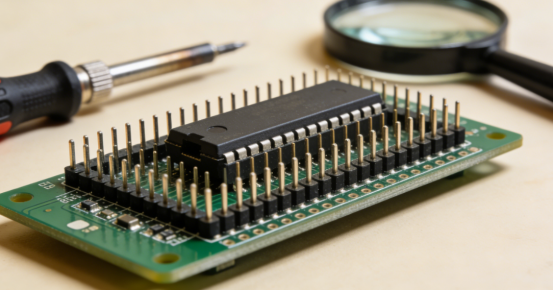
The pin configuration of a DIP is one of its most notable features. A DIP component typically has two parallel rows of pins, which extend from the sides of the package. This design makes it easy to connect the component to a PCB. The pins are inserted into small holes drilled into the PCB, and then soldered in place.
The two rows of pins make it easier for technicians to align the component and insert it into the board, reducing the chance of errors during assembly. This design also makes it ideal for breadboarding or prototyping, where quick adjustments or swaps are needed.
The pins are typically spaced 0.1 inches apart (about 2.54mm). This standard spacing makes it easy to handle the component, especially in educational settings or small projects. For example, when working with a breadboard, this 0.1-inch spacing allows the DIP to fit perfectly into the rows of holes, simplifying the circuit-building process. This is especially beneficial for beginners and hobbyists who may not have advanced tools.
Mechanical Robustness and Durability
The mechanical robustness of DIP components is another important feature. The pins are usually made of strong metal and are thicker than those found in most modern surface-mount packages, with a typical thickness between 0.6mm and 0.8mm. This thickness gives the pins greater strength and resistance to bending or breaking, making DIP a reliable choice for industrial environments and harsh conditions.
For example, in industrial machinery or factory control systems, the circuits are often subject to vibration and shocks. The thicker pins and solid construction of DIP components help them withstand these forces without losing connection. In environments like these, reliable connections are essential to prevent malfunctions or downtime.
Furthermore, because of their sturdy build, DIP components are often used in automotive electronics or other machinery that faces physical stress. Their ability to endure physical strain ensures long-term reliability, even in difficult conditions.
Easy Soldering and Replaceability
One of the biggest advantages of DIP components is how easy they are to solder and replace. The through-hole design—with pins that go through the PCB—makes it simpler to attach DIP components to the board compared to modern surface-mount components. For instance, when you’re soldering a DIP, you can access both sides of the board, which gives you a better view and more control over the soldering process. This is especially helpful for beginners or hobbyists who are just learning to solder.
If you need to replace a DIP component, it’s also easier than with SMT. The pins are visible, so you can inspect the solder joints and ensure the connection is strong. If a component needs to be swapped out, the process is straightforward, and the risk of damaging the PCB is minimized.
For example, in a DIY electronics project like building an LED matrix or a simple microcontroller circuit, the ability to easily replace a faulty DIP component can save time and effort. You simply remove the old component and insert a new one, without worrying about damaging the surrounding parts of the circuit.
Heat Dissipation and Protection
Another critical feature of DIP components is their ability to manage heat dissipation. The plastic or ceramic body of the DIP package plays a key role in spreading out and dissipating heat that is generated by the component during use. This is especially important for low-power components that may get hot during operation, such as microcontrollers or memory chips.
The larger surface area of the DIP body compared to smaller packages allows it to absorb and release heat more effectively, preventing the component from overheating. This heat protection is vital in ensuring the longevity of the component and the overall circuit, particularly in devices that run continuously, like factory control systems or audio amplifiers.
For example, in industrial applications, where machinery runs for long periods under heavy loads, managing heat is crucial. DIP components, with their built-in heat dissipation, are often preferred in such situations because they are less likely to overheat and fail.
Applications of DIP
Education and DIY Electronics
DIP components are widely used in electronics kits for students and hobbyists. A great example is the Arduino Uno, which uses DIP microcontrollers to make learning and experimentation easier. These kits are designed to help beginners get hands-on experience with circuit assembly and soldering. For someone just starting to learn about electronics, DIP is ideal because the larger pins are easier to handle, and it’s simple to see whether the soldering is done correctly.
DIP’s role in learning soldering is crucial. It helps beginners develop their skills in a way that’s more forgiving than smaller, surface-mount components. With DIP, the pins are clearly visible, making it easier to check the solder joints. This is a critical skill for any electronics enthusiast or professional. By working with DIP components, students can learn basic soldering techniques, and understand the fundamentals of circuit design and assembly before progressing to more complex technologies.
Prototyping and Development
In prototyping, DIP components offer a convenient and flexible solution. The through-hole pins make it easy to use breadboards, allowing engineers and designers to quickly test different circuit designs. For example, a microcontroller on a DIP package can be inserted into a breadboard, connected to various components, and powered up for quick testing. This hands-on approach is invaluable when experimenting with new ideas and making adjustments.
Many development platforms also rely on DIP components, including Arduino, Raspberry Pi, and various custom-built development boards. These platforms often use DIP chips for microcontrollers and integrated circuits (ICs). Because they are easy to work with, they allow developers to build prototypes without needing specialized equipment. For instance, when designing a new circuit, a designer can easily swap out DIP components to test different configurations and see how they affect the system’s performance.
Industrial and Control Systems
DIP components continue to play a significant role in industrial control systems, including factory machinery, sensors, and relay modules. In these environments, reliability and ease of maintenance are essential. The robustness of DIP pins, combined with their through-hole design, makes them a great choice for circuits that need to withstand vibrations, shocks, and other mechanical stresses.
For example, in a factory setting, a DIP component in a relay module might need to be replaced quickly if it fails. Since DIP components are easy to remove and replace, they minimize downtime. This ease of maintenance ensures that factory operations can continue without major disruptions. Additionally, because DIP components are mechanically robust, they perform well in environments where machinery is subject to frequent movement or harsh conditions.
Industries such as automotive, robotics, and manufacturing rely on DIP for control systems and sensors that monitor and regulate machinery. The straightforward assembly of DIP components makes them a reliable choice in situations where rapid repairs are necessary, and where specialized equipment may not be available.
Legacy Systems
Even in today’s digital age, legacy systems continue to depend on DIP components. These include older technologies such as arcade machines, audio amplifiers, and vintage computers. These systems, often decades old, were originally designed with DIP components because they were the most accessible and reliable option at the time.
As these systems age, it’s not always possible to replace them with modern technology, especially if the original components are no longer manufactured. In such cases, DIP components are still used for repairs or upgrades. For example, if a vintage arcade machine stops working, technicians often replace faulty DIP-based ICs to restore functionality. The simplicity of the DIP design allows for easy replacements without the need for extensive tools or expertise.
Moreover, the continued use of DIP in legacy systems is also about compatibility. Many older computing systems or audio equipment were built specifically for DIP, and upgrading them to modern packaging would require a complete redesign. By sticking with DIP components, manufacturers and repair specialists can continue servicing older technologies without compromising the integrity of the original designs.
Advantages of Using DIP Components
Simplicity in Assembly and Repair
One of the biggest advantages of DIP components is their simplicity in assembly and repair. Since DIP components have large pins that go through holes in the PCB, they are easier to work with than many modern alternatives. Unlike SMT, which requires specialized equipment like pick-and-place machines and reflow soldering for assembly, DIP components can be soldered by hand using basic tools like a soldering iron and soldering wire.
This makes DIP a perfect choice for hobbyists and low-volume production. For instance, if you’re building a small electronics project at home, you don’t need to invest in expensive machinery to assemble your circuit. Whether you're adding a microcontroller or a resistor to a circuit, DIP components can be easily inserted into the breadboard or PCB, making it possible to complete the assembly quickly and with minimal effort.
Additionally, repairing or replacing a failed DIP component is just as easy. You can simply remove the faulty part, clean the PCB, and insert the new one. This ease of replacement makes DIP ideal for maintaining older electronics, such as vintage arcade machines or audio equipment, where parts may need to be swapped regularly.
Cost-Effectiveness
DIP components are often more affordable compared to their SMT counterparts. While SMT components have the advantage of being smaller and more compact, they typically require more expensive equipment to handle, especially in high-volume production. In contrast, DIP components are cheaper to produce and assemble, making them a more cost-effective option for small-scale manufacturing or personal projects.
For example, DIY electronics kits or small production runs can save money by using DIP components. The cost of a DIP microcontroller or IC)can be 20-30% lower than an equivalent SMT part. This is particularly beneficial for projects that don’t require the compactness or high-performance characteristics of SMT. If you're just getting started with electronics or building a custom device in limited quantities, using DIP can help reduce your overall production costs.
Furthermore, manual soldering of DIP components doesn’t require expensive automated soldering machines, which is another reason for its cost-effectiveness. For anyone working with limited budgets, whether in a hobbyist setting or in small-scale electronics businesses, DIP offers a cost-saving advantage over more modern packaging options.
Physical Robustness
DIP components are known for their physical robustness, making them ideal for industrial and automotive applications. The thicker pins (usually between 0.6mm and 0.8mm) and stronger construction make them more resistant to bending, shocks, and vibrations than smaller, surface-mount components. This is especially important in environments where electronics are subject to physical stress, like in automobile circuits or factory machinery.
For example, in a car’s engine control unit (ECU), components are exposed to constant movement, temperature changes, and vibrations. A DIP component can withstand these stresses better than a smaller SMT part, reducing the likelihood of failure over time. The mechanical strength of DIP makes it suitable for harsh industrial environments, such as robotics, where components are often subject to mechanical forces and vibrations.
This durability also contributes to the long-term reliability of systems that use DIP components. In industries like aerospace or heavy machinery, where equipment must operate reliably under tough conditions, the ruggedness of DIP ensures that the components continue to function without failing prematurely.
Easier Inspection and Debugging
Another advantage of DIP components is their visibility, which makes them much easier to inspect and debug. The large pins are easy to see, and they provide clear access to the solder joints, allowing you to quickly identify potential issues like cold solder joints or poor connections. This visibility is especially important during the debugging phase of a project or when troubleshooting faulty circuits.
For instance, if a DIP component isn’t working correctly, you can visually inspect the pins and solder connections to ensure they are secure and free from defects. This is a significant benefit compared to SMT components, which are much smaller and harder to inspect. In SMT, checking solder joints often requires a magnifying glass or special tools, making the process slower and more difficult.
This ability to inspect easily also makes DIP components ideal for repair work. If something goes wrong with the circuit, technicians can quickly spot the issue and replace the faulty component, reducing downtime. In high-stakes environments, such as medical devices or critical industrial systems, where a quick response is needed, this feature can save time and money.
Challenges and Disadvantages of DIP Components
Size and Footprint
One of the main challenges of using DIP components is their larger size compared to SMT. DIP components have pins that extend through the PCB, which requires more space on the board. This makes them unsuitable for applications where space is limited, such as smartphones, wearable devices, or other compact consumer electronics.
For example, in a smartphone or tablet, the goal is to fit as many functions as possible into a small device. The larger footprint of DIP components can take up valuable space on the PCB, limiting the number of other components that can be included. SMT components, on the other hand, are much smaller and can be mounted directly onto the surface of the PCB, allowing for a more compact design. Therefore, while DIP is great for prototype circuits or hobbyist projects, it is often not a practical choice for products that require a small, slim profile.
This larger size also makes DIP less suitable for miniaturized devices, where space optimization is a top priority. As electronic devices become smaller and more powerful, DIP components face limitations in meeting the compact design requirements of modern technologies.
Slower Assembly Process
Another significant disadvantage of DIP components is the slower assembly process. Unlike SMT components, which can be placed on a PCB automatically using pick-and-place machines, DIP components require manual soldering in most cases, especially in small-scale production. This process involves inserting the pins of the component through the holes in the PCB, then applying heat and soldering the pins on the other side.
In mass production, this manual soldering process is time-consuming and inefficient compared to the high-speed automated processes used for SMT. For example, a production line can place thousands of SMT components in a matter of hours, whereas DIP assembly is limited to about 10 to 20 components per hour by hand. This slower assembly rate makes DIP less ideal for large-scale manufacturing, where high-volume production and fast assembly are essential.
For small businesses or hobbyists who need to assemble only a few units, this slower process may not be a major issue. However, for companies looking to scale up production, the time-consuming nature of manual soldering can significantly increase labor costs and delay production timelines.
Signal Integrity Issues at High Frequencies
DIP components can also face signal integrity issues when used in high-frequency applications. The long pins of DIP packages introduce inductance—a property that resists changes in current. This increased inductance can lead to signal loss, especially in circuits that need to process high-frequency signals, such as RF (Radio Frequency) circuits or 5G devices.
For example, in a 5G communication system, signals must travel at high frequencies and with minimal loss. The long pins of a DIP component can cause unwanted signal distortion, which can negatively affect the performance of the device. In contrast, SMT components are mounted directly onto the PCB, reducing the length of the pins and minimizing inductance. This makes SMT a better option for circuits requiring high-speed signal transmission and low-latency performance.
As the world moves toward faster, high-frequency applications, DIP's limitations in terms of signal quality make it less suitable for modern wireless communications, 5G networks, and other advanced technologies that require precise, high-speed data transmission.
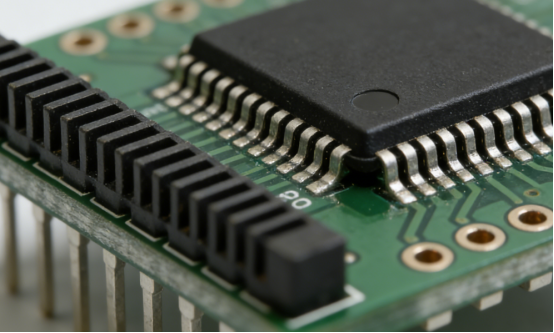
Limited Pin Count and Functionality
Another limitation of DIP components is the restricted number of pins they can accommodate. Most DIP packages are available with between 8 to 40 pins, which is sufficient for simple microcontrollers, logic gates, and analog ICs. However, this pin count is insufficient for more complex ICs or high-performance chips, such as microprocessors or high-density memory chips.
For example, modern microprocessors used in computers or smartphones typically require hundreds or even thousands of pins to handle the large number of data and power connections. A DIP component would not have the physical space to support such high-density ICs. Ball Grid Array (BGA) packages are a better choice for these applications because they offer a higher pin count and better performance in terms of both signal integrity and thermal management.
This limited pin count also restricts the functional capacity of DIP components, making them unsuitable for complex, multi-functional devices. As the demand for smaller, more powerful chips grows, DIP’s inability to accommodate these needs puts it at a disadvantage compared to more advanced packaging technologies.
DIP vs. SMT
Design and Manufacturing Considerations
When comparing DIP and SMT, the primary difference lies in their assembly methods, cost, and scalability. DIP components are inserted through holes in the PCB, with pins extending through the board and being soldered manually or with basic tools. In contrast, SMT components are mounted directly onto the surface of the PCB, using automated pick-and-place machines that place the components accurately on the board.
In terms of assembly, SMT is far more efficient for mass production. Automated machines can place thousands of SMT components per hour, whereas DIP requires manual handling for assembly, which is much slower. This makes SMT ideal for high-volume, cost-sensitive production.
DIP components, while easier to assemble manually and better suited for small-scale or prototype projects, incur higher labor costs for assembly, especially in larger quantities. However, the lower cost of assembly equipment (such as simple soldering tools) makes DIP a cost-effective option for small businesses and DIY projects.
In terms of scalability, SMT wins hands down, as it allows manufacturers to produce smaller, lighter products with much faster assembly times, thus lowering overall production costs. DIP is often used in small batches or hobbyist circuits, but SMT is the preferred technology for mass-market electronics like smartphones, laptops, and TVs.
Space Constraints in Modern Electronics
In the world of modern electronics, space is a crucial consideration. As devices become smaller, manufacturers need to pack more components into the same amount of space. This is where SMT excels. Unlike DIP, which requires larger, through-hole pins that take up space on both sides of the PCB, SMT components are much smaller and fit directly onto the surface of the board.
This space-saving ability allows SMT to be favored in miniaturized devices, such as smartphones, wearable tech, and tablets, where every millimeter counts. By using SMT, manufacturers can create compact, high-performance devices with more functionality packed into a smaller form factor.
For instance, in a smartphone, the use of SMT components means that all the necessary parts, like processors, memory, and connectors, can be placed closely together, enabling the device to be slim, sleek, and powerful. DIP components, with their larger footprint, cannot achieve the same miniaturization and density, which makes them impractical for these kinds of space-constrained applications.
In contrast, DIP remains useful in situations where compactness is not as critical, such as in educational kits or legacy systems that don’t require miniaturization but benefit from easy assembly and manual handling.
Durability and Maintenance
While SMT has its advantages in terms of space and mass production, DIP components offer significant benefits in terms of durability and maintenance. DIP components are generally more robust and easier to replace. Since the pins are larger and extend through the PCB, they are less susceptible to damage from physical shocks or vibrations, which makes them ideal for environments like factory machinery or automotive electronics where components need to be frequently replaced or repaired.
In industrial environments, where maintenance is common, the ability to easily replace a failed component without damaging the entire circuit is a major advantage. DIP components allow technicians to manually remove and replace parts without specialized equipment. This repairability is especially useful in settings like robotics, legacy systems, and old audio equipment, where parts need to be swapped out frequently and without the risk of damaging the surrounding circuitry.
On the other hand, SMT components are often smaller and fragile, making manual repair more difficult. Because SMT components are mounted directly on the surface of the PCB, they require more precision tools and techniques for removal and replacement. Additionally, SMT components are often more difficult to inspect visually, which can make identifying faults or damage more challenging.
Comparison Table: DIP vs. SMT
Feature DIP SMT Assembly Method Manual soldering with pins through the PCB Automated machine placement on PCB surface Cost Lower for small-scale production and prototyping Lower for large-scale production, higher for machines Size/Footprint Larger, takes up more space on the PCB Smaller, ideal for miniaturized devices Space Efficiency Requires space on both sides of the PCB Highly space-efficient, enabling compact designs Durability More durable, less likely to suffer from mechanical stress More fragile, may require specialized tools for repair Repairability Easier to replace and repair manually Harder to repair manually due to smaller size and soldering difficulty Scalability Suitable for small runs and DIY projects Ideal for mass production and large-volume applications Signal Integrity Good for low-frequency and simple applications Better for high-frequency applications, but more sensitive to heat and stress
Choosing Between DIP and Other Package Types
When to Choose DIP
DIP (Dual Inline Package) is an excellent choice in specific scenarios, primarily where ease of assembly, repairability, and cost-effectiveness are key priorities. Here are some ideal situations for using DIP components:
1. Prototyping and DIY Projects
DIP components are perfect for prototyping, particularly when working on small-scale electronics or experimental circuits. Their larger size and through-hole design make them easier to handle and work with, especially for those new to electronics. For instance, if you're building a custom circuit on a breadboard or development board, using DIP components allows you to quickly swap parts in and out during testing without the need for specialized equipment. They are also ideal for hobbyists and students working on electronics kits, such as those used in Arduino or Raspberry Pi projects.
2. Education
DIP components remain a favorite in education because they allow students to see and understand the mechanics of a circuit. The visible pins make it easy to inspect solder joints, which is crucial when learning the basics of soldering. Using DIP components for circuit-building activities helps beginning engineers and students grasp foundational concepts like component placement and troubleshooting.
3. Industrial Repairs and Legacy Systems
DIP components are often found in legacy systems and industrial machinery. They are easier to replace manually, which is essential in environments where equipment is outdated or regularly serviced. In industries such as manufacturing, audio equipment repair, or vintage computers, DIP components can be swapped out without requiring specialized equipment. This makes maintenance more straightforward and cost-effective in settings where component replacement is frequent.
When Not to Choose DIP
While DIP has its advantages, there are several scenarios where it may not be the best choice. Here’s when other packaging types, such as SMT (Surface-Mount Technology) or BGA (Ball Grid Array), might be more suitable:
1. Miniaturized Devices
For devices that need to be as compact and space-efficient as possible, such as smartphones, wearables, and laptops, SMT is the preferred option. SMT components are smaller, allowing more components to fit on a single PCB, making them ideal for miniaturized devices that require high-density layouts.
2. High-Performance, High-Frequency Applications
If you're working with high-frequency circuits, such as 5G, RF (Radio Frequency) systems, or signal processors, DIP components may not be the best choice. The long pins in DIP create inductance, which can cause signal degradation and reduce the performance of the circuit. In these cases, SMT or BGA (which has shorter electrical connections) is a better choice as they help reduce inductance and maintain signal integrity.
3. High Pin Count or Complex ICs
For devices requiring a high pin count, like advanced microprocessors, memory chips, or complex ICs, DIP is limited. Most DIP packages can handle only up to 40 pins, which is insufficient for modern, high-density integrated circuits. In such cases, BGA packages, which can support hundreds or even thousands of pins, are preferred. BGA packages also provide better thermal performance and electrical connections, making them suitable for high-end processors and GPUs.
4. Mass Production
In large-scale manufacturing, SMT components are preferred because they can be placed on the PCB quickly and accurately using automated equipment. DIP components require more manual labor, which increases the time and cost of assembly. If you’re building products in high volumes, SMT is much more efficient and cost-effective, making it the go-to option for mass-market electronics like smartphones, televisions, and computers.
Hybrid Approaches
In some cases, it makes sense to combine DIP and SMT components in a single design. A hybrid approach can take advantage of the strengths of each packaging type to meet specific requirements of the project. Here’s how:
1. DIP for Specific Components
In a mixed-technology design, DIP components might be used for parts that require manual soldering or frequent replacement. For instance, you could use DIP for connectors, switches, or small integrated circuits that might need maintenance or repair. These parts are easy to work with and can be manually replaced when needed.
2. SMT for Small, High-Density Components
The rest of the circuit can be designed using SMT, especially for high-performance components like processors, memory chips, or power management ICs. These components are smaller, fit into tighter spaces, and are better suited for mass production.
3. Hybrid Designs in Prototyping
In the prototyping phase, a designer may use DIP components for easy testing and quick iterations, while the final design might shift to SMT to reduce size and increase production efficiency. This hybrid method is often seen in the transition from early-stage prototypes to final products.
4. Industrial Applications
In industrial machinery or automation systems, a hybrid approach could involve using DIP components for user-accessible controls or interface modules, while more complex internal components are placed using SMT or BGA for better performance and durability.
Conclusion
DIP continues to offer significant advantages, especially in prototyping, education, and repair environments. Its easy assembly, durability, and cost-effectiveness make it a popular choice for hobbyists and small-scale production. However, its larger footprint, slower assembly, and limitations with high-frequency applications make it less suitable for modern, miniaturized devices and mass production.
Despite the rise of SMT and BGA, DIP remains relevant in specific sectors, particularly for legacy systems and situations where manual repairs are required. The future of DIP may be limited, but it will likely continue to play a role in applications where ease of use, maintenance, and repairability are prioritized over size and high-frequency performance.
If you have more questions or want to dive deeper into PCB technology, feel free to contact PCBMASTER. As an experienced PCB supplier, we are always ready to assist with expert insights and guidance.
FAQs
What is the main advantage of using a DIP component?
The main advantage of DIP components is their ease of manual assembly. Their large pins and simple design make them ideal for hobbyists, prototyping, and small-scale production. The robust physical design also makes them more durable in certain environments, offering greater resistance to physical stress and easier replacement in systems that require regular maintenance. This makes DIP an excellent choice for projects where components need to be manually inserted and swapped without specialized equipment.
Why is DIP less commonly used in modern smartphones and tablets?
DIP is not commonly used in modern smartphones and tablets due to its space and performance limitations. The large footprint of DIP components takes up more PCB space, which is a major issue in compact mobile devices that require smaller, more densely packed boards. Additionally, SMT offers better high-frequency performance and is more suitable for miniaturized circuits. Modern devices prioritize size, efficiency, and performance, which makes SMT the preferred choice in mobile electronics.
Can DIP components be used in high-frequency circuits?
Using DIP components in high-frequency circuits can present challenges. The long pins in DIP packages introduce inductance, which resists changes in electrical current. This inductance can cause signal loss, making it unsuitable for applications that require precise, high-speed signal transmission, like 5G or RF circuits. In such cases, SMT or BGA packages, which have shorter electrical connections and better signal integrity, are better suited for high-frequency designs.
Is it possible to use DIP in automated production lines?
While DIP components can technically be used in automated production lines, they are less efficient compared to SMT components. DIP components require through-hole placement and manual soldering in many cases, which increases assembly time and cost. Automated machines designed for SMT can place and solder thousands of components quickly and accurately, making DIP less suitable for high-volume production. Although DIP is cost-effective for small batches, it is not as scalable or efficient for mass production.
How do I solder a DIP component on a PCB?
Here’s a step-by-step guide for soldering a DIP component on a PCB:
1. Preparation: Insert the DIP component through the holes of the PCB, ensuring that the pins align with the pads on the board.
2. Secure the component: Gently bend the pins outward slightly to hold the component in place.
3. Soldering the pins: Heat your soldering iron to about 350°C (662°F). Touch the tip of the iron to one of the pins and the corresponding pad on the PCB, then apply solder to the joint. Remove the soldering iron and allow the joint to cool.
4. Check the solder joints: Inspect the solder joints to ensure they are clean and solid. They should have a shiny appearance and be free from cold joints (dull or cracked solder).
5. Repeat: Continue soldering the remaining pins, moving in a consistent pattern to avoid overheating any part of the PCB.
6. Trim excess pins: Once all the pins are soldered, use wire cutters to trim any excess pin lengths that extend beyond the PCB.
Tips for beginners: If you're new to soldering, start by practicing on a spare PCB or a simple project before working on your main project. Be patient, and ensure that the iron tip is clean for effective soldering.
Author Bio
Hi, I'm Carol, the Overseas Marketing Manager at PCBMASTER, where I focus on expanding international markets and researching PCB and PCBA solutions. Since 2020, I've been deeply involved in helping our company collaborate with global clients, addressing their technical and production needs in the PCB and PCBA sectors. Over these years, I've gained extensive experience and developed a deeper understanding of industry trends, challenges, and technological innovations.
Outside of work, I'm passionate about writing and enjoy sharing industry insights, market developments, and practical tips through my blog. I hope my posts can help you better understand the PCB and PCBA industries and maybe even offer some valuable takeaways. Of course, if you have any thoughts or questions, feel free to leave a comment below—I'd love to hear from you and discuss further!

