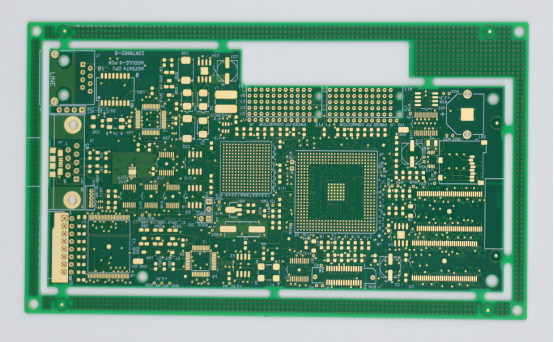
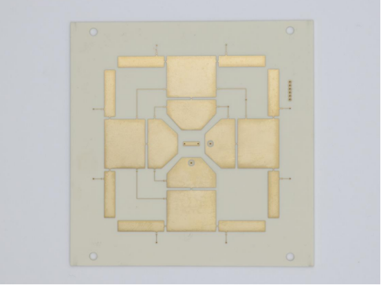
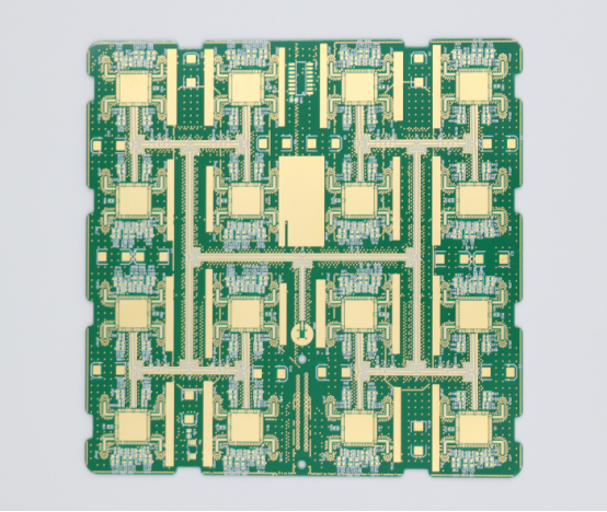
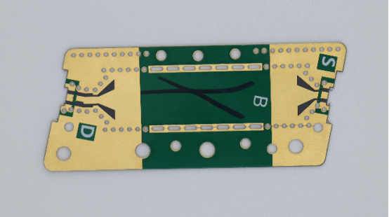
How to Resolve Design and Manufacturing Conflicts in HDI PCB Production
High-Density Interconnect (HDI) PCBs are crucial for modern electronics, enabling compact devices like 5G smartphones and medical equipment. They allow more components to fit into smaller spaces, improving performance and efficiency. However, the gap between design goals and manufacturing capabilities often causes issues like production delays, defects, and higher costs. Designers may push for advanced features, but manufacturers might struggle with the equipment or materials needed to meet those requirements.
This article aims to help designers and engineers identify these design-manufacturing conflicts early. By understanding common issues and implementing solutions, teams can avoid costly mistakes, improve product quality, and ensure smoother production. Whether you're designing simple or complex HDI PCBs, this guide provides practical tips for optimizing both design and manufacturing.

Main Causes of Design and Manufacturing Conflicts in HDI PCB
1. Design Goals and Manufacturing Capabilities Mismatch
One of the most common causes of HDI PCB production issues is a mismatch between the design specifications and the capabilities of the manufacturing equipment. HDI designs often include very fine features like small traces, microvias, and multiple stacked layers, which require high precision. However, not all manufacturers can achieve the level of accuracy needed for these features.
Example: A design with 4-mil traces or 6-mil microvias may look great on paper, but many PCB manufacturers use equipment that can only handle 8-mil traces and 10-mil vias. This discrepancy can lead to misalignment, weak connections, or even complete board failure. If the design requires 12 layers but the manufacturer can only handle 8, the stackup may need to be reworked, leading to delays and increased costs.
Solution: Designers should collaborate with manufacturers early in the process to ensure their design is within the limits of the manufacturing capabilities. This collaboration can help avoid costly redesigns and ensure a smooth production process. Additionally, incorporating Design for Manufacturability (DFM) checks during the design phase can catch these mismatches before they become major issues.
2. Documentation Errors and Inconsistencies
Inaccurate or inconsistent documentation is another major cause of delays and production errors in HDI PCB manufacturing. Gerber files, drill drawings, and other documentation need to align perfectly with the design specifications and the manufacturer’s capabilities. Even small discrepancies between the documentation and the actual design can cause significant issues in production.
Example: If the Gerber files are missing important layer information or the drill file doesn’t match the hole sizes specified in the design, this can cause misalignment during manufacturing. Additionally, outdated or incorrect material specifications, such as copper weight or dielectric thickness, can lead to quality problems, including signal loss or thermal failure.
Solution: Always double-check Gerber files and drill drawings before sending them to the manufacturer. Use tools to verify the alignment of all layers and ensure that all material specifications are up to date and match the manufacturer’s capabilities. Regular audits and DFM checks are essential for catching these issues early and reducing production delays.
3. Incorrect Material Selection
Choosing the wrong materials for an HDI PCB can significantly impact its performance and reliability. Materials like copper weight and dielectric materials must be carefully selected to meet the electrical and thermal requirements of the design. If the materials don't meet industry standards (like those set by IPC), it can lead to failure under certain conditions, such as thermal cycling or high-frequency operation.
Example: Using a low-quality dielectric material that doesn’t handle heat well can lead to PCB failure in high-temperature environments. Similarly, using copper with an incorrect thickness can affect the board’s signal integrity, leading to issues like power loss or crosstalk.
Solution: Always choose materials that meet IPC standards and are appropriate for the application. High-temperature laminates, for example, should be used in designs that will experience thermal stress. If unsure, consult with your manufacturer to select materials that align with the design requirements and ensure optimal performance.
4. Designs Beyond Manufacturing Capabilities
Sometimes, a design may require features that simply exceed what the manufacturer’s equipment can handle. This includes specifications like very small hole diameters, complex multi-layer stackups, or tight tolerance requirements. When designs exceed these capabilities, the result is often manufacturing failure or the need for costly workarounds.
Example: A design might specify 4-mil microvias, but the manufacturer’s laser drilling equipment is limited to 6-mil vias. This can lead to failed connections, particularly in high-speed applications like 5G boards, where precise microvias are critical. Similarly, stacking too many layers can create alignment issues during lamination.
Solution: During the design phase, communicate clearly with the manufacturer about their equipment limitations. Choose design features that are compatible with their capabilities, or adjust the design to fit within the manufacturing constraints. Prototyping can also help identify issues early, allowing for quick adjustments before full-scale production.

How to Identify and Avoid Design and Manufacturing Conflicts in HDI PCBs
1. Early Communication with Manufacturers
One of the key ways to avoid design and manufacturing conflicts in HDI PCBs is by starting communication with manufacturers early. Discussing the design details at the beginning can help ensure that the design is manufacturable and that both the design team and manufacturer are aligned. Early communication reduces the chances of errors or changes later that could cause delays or increased costs.
Action Steps:
Schedule design kickoff meetings with the manufacturer to go over stack-up structures, microvia plans, and component lists.
Confirm design specifications such as microvia sizes, trace widths, and spacing to ensure they fit within the manufacturer's equipment limits.
Example: For instance, if the microvia size exceeds what the manufacturer can handle, it could result in misalignment or defects. Confirming this early helps avoid such issues during production.
2. Follow DFM
To ensure a smooth manufacturing process, it is essential to adhere to standard HDI design rules. These rules help ensure that the design can be produced with the available technology and manufacturing processes. Following these rules minimizes the risk of errors and improves the overall quality of the PCB.
Key Design Rules for HDI PCBs:
Line width: Between 2-4 mils
Microvia diameter: Between 6-8 mils
Microvia aspect ratio: ≤ 0.75:1
Layer spacing: Ensure it complies with the manufacturer's maximum tolerances.
Action Steps:
Use Design Rule Checking (DRC) tools to identify potential errors during the design phase.
Continuously validate that the design meets these rules, adjusting as necessary.
Example: If a microvia diameter is too small for the manufacturer’s equipment, it may not be drilled properly, resulting in defects that can delay production.
3. Conduct Regular DFM Checks
DFM checks are essential throughout the design process. These checks ensure that the design is feasible to produce without errors or unexpected issues. By catching problems early, the manufacturing process will be smoother, saving time and money.
Things to Check During DFM:
Microvia spacing and clearance
Pad size and clarity
Solderability and via filling
Alignment of layers
Action Steps:
Run DFM checks frequently during the design process to ensure all elements meet manufacturing standards.
Make sure there are no issues that could cause production delays or quality concerns.
Example: If the via filling is inadequate, the solder joints could fail during assembly, leading to faulty connections. A quick DFM check can catch such issues early.
4. Thorough Gerber File Review
Before sending the design files to the manufacturer, it’s important to review the Gerber files carefully. These files are the blueprint for manufacturing, and errors in the Gerber files can lead to production mistakes, delays, or quality issues.
Common Gerber File Issues:
Incorrect file formats
Misaligned layers
Missing data (e.g., no copper layer or drill file)
Action Steps:
Use Gerber file viewers to ensure the integrity of the files.
Check that the files conform to the manufacturer’s preferred format (e.g., RS-274X).
Compare the Gerber files with the Bill of Materials (BOM) to ensure everything is accounted for.
Example: If a drill layer is missing from the Gerber files, the manufacturer will not know where to drill the vias, causing delays or rework.
5. Continuous Feedback and Iteration
Feedback and iteration are crucial throughout the design process. Regular collaboration with manufacturers allows you to adjust designs and resolve issues before they become serious problems.
Action Steps:
Share design progress regularly with the manufacturer for feedback.
After each design update, conduct DFM checks to ensure the changes are manufacturable.
Iterate based on feedback, revising the design to fit the manufacturer’s capabilities.
Example: A manufacturer might point out that a particular layer spacing is too tight. By receiving this feedback early and making adjustments, you can avoid delays in the later stages of production.
6. Microvia Design Optimization
Microvias are a critical component in HDI PCBs, but they can also introduce reliability issues if not designed correctly. Optimizing microvia design ensures that the board performs well without structural weaknesses.
Key Microvia Design Factors:
Maintain a depth-to-diameter ratio of ≤ 0.75:1.
Use laser drilling for precise and clean microvias.
Choose surface finishes like ENIG (Electroless Nickel Immersion Gold) or ENEPIG (Electroless Nickel Electroless Palladium Immersion Gold) to enhance solderability.
Action Steps:
Keep the depth-to-diameter ratio within the recommended limits to avoid fragile vias.
Select an appropriate surface finish to improve solder joint reliability.
Example: Microvias with a high depth-to-diameter ratio are more likely to crack or fail under thermal stress. By ensuring proper ratios and surface finishes, you enhance the board's durability.
7. Ensure Signal Integrity and EMC Compliance
In HDI PCBs, especially those used in high-frequency applications, ensuring signal integrity and electromagnetic compatibility (EMC) is critical. Poor signal quality or electromagnetic interference (EMI) can cause devices to malfunction.
Solutions for Signal Integrity and EMC:
Use signal integrity simulation tools (e.g., Keysight ADS) to check that signal paths and trace widths are correct.
Apply 3D electromagnetic field simulation tools (e.g., Ansys HFSS) to reduce EMI and improve EMC compliance.
Action Steps:
Perform signal integrity simulations early to ensure the design meets performance criteria.
Use EMI reduction techniques and materials to minimize interference.
Example: If the trace width for high-speed signals is too narrow, signal degradation can occur. Using simulation tools early in the design phase can help avoid such issues.

How to Effectively Validate HDI Designs
1. HDI Prototype Validation
Validating HDI designs through prototypes is essential for ensuring that the design can be manufactured without issues. Prototypes help identify manufacturing problems early, preventing costly and time-consuming mistakes in full-scale production.
Why Prototype Validation is Important:
Prototypes allow you to test your design in real-world conditions, identifying potential issues that might not be visible in simulations. This early testing helps avoid problems like weak vias, poor alignment, or thermal issues that could affect the final product's reliability.
Prototype Validation Steps:
Choose Complex Areas for Testing: Focus on challenging parts of the design such as microvia clusters and BGA (Ball Grid Array) areas. These areas are often prone to issues, so they should be prioritized for validation.
Test Electrical, Mechanical, and Thermal Performance: Ensure that the prototype performs well under all conditions. Electrical tests check signal integrity, mechanical tests assess the board’s physical strength, and thermal tests ensure that heat dissipation is adequate.
Example: If the prototype reveals poor thermal performance in certain areas, adjustments can be made to the design before mass production, saving both time and costs.
2. Rapid Prototyping and Feedback
Using rapid prototyping allows for faster feedback, which is critical to refining the HDI design. By producing prototypes quickly, you can test the design, gather feedback, and make necessary adjustments without significant delays.
How to Use Rapid Prototyping:
Use Specialized HDI Prototyping Equipment: Technologies like laser drilling and sequential lamination are commonly used in HDI prototype production. These methods help produce small runs of prototypes quickly and accurately.
Iterative Feedback and Testing: Once the prototype is produced, it undergoes rigorous testing. Based on the feedback from these tests, design adjustments can be made rapidly, followed by another round of prototype production to verify those changes.
Feedback Loop:
The iterative nature of rapid prototyping ensures that issues are caught early, and design changes are implemented efficiently. Regular feedback from the manufacturer and testing phase will guide the final design toward being manufacturable with minimal risk.
Example: Suppose the first round of prototypes shows that a specific layer stack-up is causing alignment issues. The design can be quickly adjusted and tested again, ensuring that the final product will meet manufacturing standards.

Conclusion
To ensure high-quality production and prevent costly mistakes, it is crucial for designers and manufacturers to collaborate closely from the very beginning of the design process. By aligning design goals with manufacturing capabilities, performing regular DFM checks, and continuously iterating based on prototype feedback, teams can significantly reduce the risk of conflicts between design and manufacturing. This proactive approach leads to smoother production cycles, fewer revisions, and ultimately, more reliable and cost-effective HDI PCBs.
As the industry moves towards more advanced and efficient solutions, companies like PCBMASTER are at the forefront, utilizing cutting-edge technologies to bridge the gap between design and manufacturing. Their expertise in HDI technology, combined with rapid prototyping and fast delivery times, ensures that your designs transition smoothly from concept to production. With a focus on performance, quality, and cost, PCBMASTER is well-equipped to meet the evolving demands of modern electronics. Whether for prototyping or mass production, their robust capabilities make them a trusted partner in bringing innovative products to life.
FAQs
1. What are the most common mistakes in HDI PCB design?
The most common mistake in HDI PCB design is failing to collaborate early with the manufacturer. This often leads to designs that are not manufacturable, typically due to issues like microvia sizes being too small or line widths being too narrow. Early communication with the manufacturer helps identify potential issues before they become costly problems during production.
2. How can I ensure my HDI design meets manufacturing standards?
To ensure your HDI design aligns with manufacturing standards, start by collaborating with the manufacturer early in the design process. Understand their manufacturing capabilities and perform regular DFM checks throughout the design cycle. This ensures that all design elements, such as microvia sizes, trace widths, and layer alignment, are within the acceptable range for production.
3. Why is microvia design so important?
Microvia design is crucial in HDI PCB construction because errors in this area can affect the board's reliability. For instance, a high aspect ratio (the ratio of the depth to diameter of a via) can cause uneven via walls, making the board more prone to cracks and compromising its strength and durability. Properly designed microvias ensure the structural integrity of the PCB and its long-term performance.
4. How can I avoid Gerber file errors?
To avoid Gerber file errors, use a Gerber viewer to carefully check each layer for alignment, drill sizes, and completeness. Ensure the file format is consistent with the manufacturer’s requirements, such as RS-274X, and double-check that all components are correctly aligned, with no missing or duplicate layers. This thorough review will minimize the risk of errors during production and save time and resources.
5. What are the benefits of HDI prototype validation?
HDI prototype validation is invaluable because it helps identify potential manufacturing issues before mass production begins. By testing a prototype, you can uncover issues such as poor via alignment or thermal performance problems, which can be adjusted before they lead to costly production delays. Prototyping helps refine the design, ensuring smoother production runs and reducing time and cost in the long run.
Author Bio
Hi, I'm Carol, the Overseas Marketing Manager at PCBMASTER, where I focus on expanding international markets and researching PCB and PCBA solutions. Since 2020, I’ve been deeply involved in helping our company collaborate with global clients, addressing their technical and production needs in the PCB and PCBA sectors. Over these years, I’ve gained extensive experience and developed a deeper understanding of industry trends, challenges, and technological innovations.
Outside of work, I’m passionate about writing and enjoy sharing industry insights, market developments, and practical tips through my blog. I hope my posts can help you better understand the PCB and PCBA industries and maybe even offer some valuable takeaways. Of course, if you have any thoughts or questions, feel free to leave a comment below—I’d love to hear from you and discuss further!


