Complete Guide to the PCB Assembly Process: From Soldering to Final Testing
Imagine a world where every electronic device, from your smartphone to life-saving medical equipment, operates flawlessly—each component working in perfect harmony. But this seemingly seamless performance is the result of a highly sophisticated and precise process: PCB assembly. Behind the scenes, layers of technology and meticulous attention to detail are at play, ensuring that every connection is solid, every component correctly placed, and every circuit ready to perform under the most demanding conditions.
In the intricate dance of PCB assembly, every step matters. The quality of solder joints, the placement of tiny components, and even the testing methods used can make the difference between a device that works perfectly and one that fails under pressure. This journey—spanning from the initial design to final testing—is not just about building a circuit board; it’s about crafting the foundation for the next wave of innovation in electronics. As we dive deeper into this process, we’ll explore the technologies, techniques, and key factors that drive the assembly of high-performance, reliable electronic devices.
Introduction to PCB Assembly
What is PCB Assembly?
PCB assembly is the process of connecting electronic components to a printed circuit board (PCB) to create a fully functional electronic product. This process is fundamental to the manufacturing of all modern electronic devices, enabling them to perform the specific tasks they were designed for. Without proper PCB assembly, even the most sophisticated electronics wouldn't be able to function, as the PCB serves as the backbone that connects all the components.
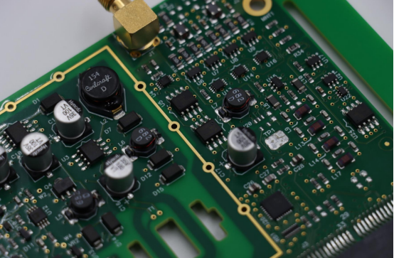
At its core, PCB assembly involves placing components like resistors, capacitors, chips, and connectors onto a PCB, and ensuring they are electrically and mechanically integrated through processes such as soldering. The assembly transforms a simple board with copper traces into a working circuit capable of transmitting signals, power, and data.
Real-world Examples of PCB Assembly:
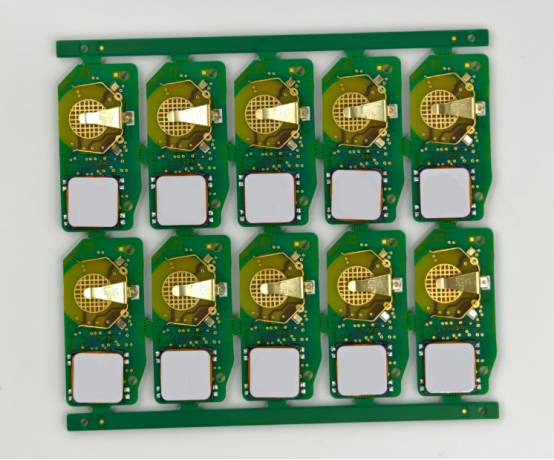
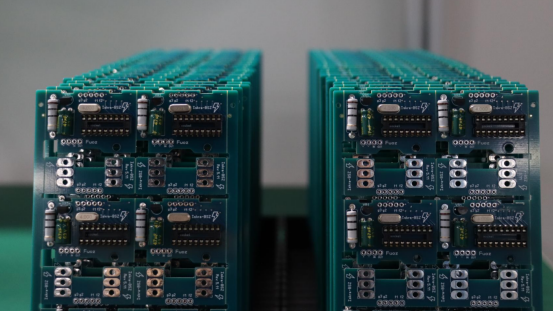
Smartphones and Laptops: These devices contain intricate PCBs that handle everything from processing data to powering the screen. The assembly process ensures that each tiny component, often smaller than a grain of rice, is correctly placed to create the device’s full functionality.
Medical Devices: In life-saving equipment like pacemakers, the PCB assembly process ensures that all components are precisely aligned and reliably connected, as failure could have dire consequences. Each solder joint and placement is meticulously checked to meet stringent standards.
Overview of the PCB Assembly Process
The PCB assembly process is a multi-stage journey that starts with a bare PCB and ends with a fully functional electronic device. Each stage plays a crucial role in ensuring the final product is reliable, efficient, and ready for use in various applications. Below is a high-level breakdown of the key stages involved in PCB assembly:
1. Solder Paste Printing:
The first step in the process is printing solder paste onto the PCB. This paste, a mixture of tiny metal particles and flux, is applied to the PCB pads where components will be placed. The precision of this step is critical because an improper paste application can lead to poor solder joints.
2. Component Placement:
Once the solder paste is applied, the next step involves placing components onto the board. This is typically done using automated machines that pick and place components with incredible accuracy. The placement must be precise to ensure each component is aligned with the corresponding pads for soldering.
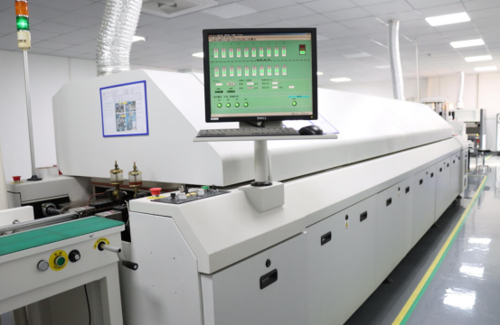
3. Reflow Soldering:
After the components are placed, the PCB is heated in a reflow oven. This process melts the solder paste, forming solid solder joints that electrically and mechanically bond the components to the PCB. Proper temperature control during reflow is essential to avoid damaging sensitive components or creating faulty solder joints.
4. Inspection and Testing:
After soldering, the PCB undergoes inspection to check for defects like solder bridges, cold joints, or misalignment. Automated Optical Inspection (AOI) and other testing methods are used to ensure the board meets quality standards. Electrical testing checks that each connection is intact and functioning as expected.
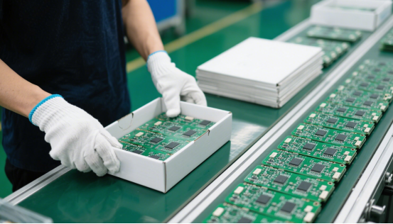
5. Final Packaging:
Once the PCB passes inspection and testing, it’s ready for final packaging. In this stage, the PCB is prepared for integration into the final product, whether it’s a consumer device, industrial equipment, or medical instrument.
Each of these stages is critical to ensuring that the final product meets both performance and reliability standards. Any flaws in the process can lead to device malfunctions, highlighting the importance of precision and quality control throughout the entire PCB assembly process.
Key Stages in PCB Assembly
Solder Paste Printing
Step-by-Step Process
Stencil Application: Solder paste is applied to the PCB’s pads using a metal stencil. The stencil has openings that match the locations of the components on the board. A scraper or squeegee spreads the paste evenly over the stencil, depositing the paste onto the PCB pads.
Precision Paste Deposition: The amount and accuracy of solder paste applied are critical to the success of the soldering process. Too much paste can cause solder bridges or shorts, while too little can result in weak or incomplete solder joints.
Challenges and Solutions
Insufficient or Excess Paste: If there is too little paste, components may not be adequately soldered, leading to weak joints or cold solder joints. Conversely, excess paste can cause bridges between pads, resulting in short circuits.
- Solution: To avoid this, it's essential to fine-tune the paste printing process. Regular inspection of the stencil, as well as the use of precise equipment, can help achieve uniform and controlled paste deposition.
Impact of Paste Quality on Reliability: The quality of the solder paste plays a significant role in the reliability of solder joints. Poor-quality paste can lead to poor wetting, which weakens the connection, or it can cause voids inside the solder joints, compromising electrical performance.
- Solution: Using high-quality solder paste, ideally formulated for the specific components and board design, can help maintain the integrity of the joints.
Examples and Considerations
Lead-Free vs. Leaded Solder Paste:
Lead-Free Paste: These pastes are commonly used today due to environmental regulations (e.g., RoHS compliance). They typically use alloys such as Sn-Ag-Cu, which have higher melting points and may require slightly different processing conditions than leaded pastes.
Leaded Paste: While still in use for certain applications, leaded solder paste (typically Sn-Pb) has a lower melting point and is easier to work with but is gradually being phased out in favor of lead-free alternatives.
Component Placement
Machine vs. Manual Placement
Automatic Pick-and-Place Machines: These machines are the heart of modern PCB assembly. They use robotics and vision systems to place thousands of tiny components accurately and quickly onto the board. This method is fast, efficient, and highly precise, making it ideal for large-scale production runs.
- Benefits: Speed, consistency, and accuracy. Automatic machines can place components at a rate of thousands per hour with high precision, reducing the risk of human error.
Manual Placement: Despite automation, manual placement is still necessary for large or irregularly shaped components that automated machines cannot handle, such as transformers or connectors. Manual placement is also common for low-volume or prototype runs.
- When Necessary: Manual placement is most effective when the board contains components that are too large or delicate for the pick-and-place machine to handle or when a small batch needs to be assembled.
Component Orientation and Accuracy
Proper Placement for Solder Joint Quality: Ensuring each component is placed in the correct orientation is essential for the performance and longevity of the device. Incorrect placement can lead to faulty solder joints, signal interference, or mechanical failure.
Common Placement Errors: Misalignment of components or incorrect orientation can cause issues such as:
- Short Circuits: If the leads of a component are placed too close together or on incorrect pads, they may form unintended connections, leading to a short.
- Reduced Functionality: Components like resistors or capacitors may not work effectively if they are not placed according to the design specifications, impacting the overall circuit performance.
Reflow Soldering
Principles of Reflow Soldering
Reflow soldering is a heating process that melts the solder paste to form solid solder joints, bonding components to the PCB. This process involves passing the PCB through a reflow oven where temperatures gradually rise to the melting point of the solder.
Four-Stage Temperature Profile:
1. Preheat Stage (100-150°C): Gradual heating to avoid thermal shock to the components and PCB.
2. Soak Stage (150-180°C): Flux activation and the removal of oxides from the pads and component leads.
3. Reflow Stage (Peak Temp: Lead-Free ~240-260°C, Leaded ~210-230°C): The solder paste melts, forming the solder joints.
4. Cooling Stage (Below 100°C): Rapid cooling to solidify the solder joints and avoid defects like coarse grain formation.
Factors Affecting Reflow Quality
Oven Settings: Temperature accuracy and uniformity across the oven are essential for high-quality solder joints. If the temperature varies too much, certain areas of the PCB may overheat, damaging components or underheating, causing incomplete soldering.
- Solution: Regular calibration and monitoring of the reflow oven help maintain consistent temperature profiles and ensure uniform heating.
Solder Paste and Component Compatibility: Not all solder pastes are the same, and different components may require different heating profiles. For example, temperature-sensitive components like plastic packages need careful temperature control to avoid melting or warping.
- Solution: Use solder paste and components that are compatible with the chosen reflow profile. Ensure that both are rated for the same temperature ranges to prevent issues during the process.
Lead-Free Soldering Challenges
Higher Temperatures Required: Lead-free soldering typically requires higher reflow temperatures than traditional leaded soldering due to the higher melting points of lead-free alloys. This can place additional stress on components and increase the risk of component damage or thermal shock.
- Implications: Manufacturers need to adjust their reflow profiles to account for the higher temperatures needed for lead-free solder. This could also affect the choice of components, as certain materials may not be as resistant to these higher temperatures.
- Solution: Advanced ovens with precise temperature control can handle lead-free soldering challenges by ensuring that each stage of the reflow process is carefully calibrated to avoid thermal damage.
By understanding these key stages in PCB assembly—solder paste printing, component placement, and reflow soldering—manufacturers can optimize the process for reliability and efficiency. Each step requires careful attention to detail, as small deviations can impact the quality of the final product.
Inspection and Testing in PCB Assembly
Automated Optical Inspection (AOI)
Role of AOI in Quality Control
Detecting Soldering Defects: AOI plays a crucial role in identifying common soldering issues such as voids, cold joints, and bridging. These defects can severely impact the performance of the PCB, and detecting them early in the process helps prevent faulty products from moving to the next stages.
- Voids: Empty spaces within the solder joints that can affect electrical conductivity.
- Cold Joints: Weak or incomplete solder connections that may result in intermittent or failed circuits.
- Bridging: Excess solder connecting adjacent pads, which can lead to short circuits.
Precision Before Functional Testing: AOI helps ensure that the PCB assembly is free from basic visual defects, allowing the functional testing stages to focus on more complex performance issues. By catching errors early, AOI ensures that only properly assembled boards move on to the next steps, which improves overall efficiency.
How AOI Works
High-Resolution Imaging: AOI uses high-resolution cameras to capture detailed images of the PCB after soldering. These images are then compared to predefined templates that represent the ideal PCB assembly.
Defect Recognition Algorithms: Advanced algorithms analyze these images to detect discrepancies, such as misaligned components or soldering defects. The system can automatically flag areas that require attention, marking the defective regions for further inspection or rework.
Limitations and Advantages
Advantages of AOI: AOI excels at inspecting visual and mechanical soldering quality, ensuring that surface-level defects like missing or misaligned components, solder bridges, and insufficient solder are caught before moving forward.
Limitations of AOI: While AOI is effective at detecting surface-level issues, it struggles to detect defects hidden beneath components, such as poor electrical connections or solder joints that are not visible. As a result, it cannot fully guarantee the integrity of the PCB without further testing.
In-Circuit Testing (ICT)
How ICT Identifies Electrical Defects
Electrical Performance Checks: ICT focuses on testing the electrical characteristics of components and the connections between them. By probing specific test points on the PCB, it can verify that each component functions correctly and that there are no open circuits or shorts.
- Open Circuits: Occur when a component or connection is missing, preventing electrical current from flowing.
- Component Misplacement: ICT can identify whether components are in the correct location and orientation.
- Parameter Deviations: It can detect component parameters (e.g., resistance, capacitance) that deviate from the intended specifications, indicating potential failure.
Benefits and Limitations of ICT
High Detection Accuracy: ICT is highly effective at detecting electrical defects, ensuring that all components are properly placed and functioning. It can catch issues that AOI might miss, such as incorrect component values or faulty connections.
Customized Fixtures Required: ICT requires customized test fixtures that align with the specific PCB design. This means that each new product or design may require a unique fixture, which can be time-consuming and costly to set up.
Limited Functional Testing: While ICT is excellent at identifying electrical issues, it cannot assess the overall functional performance of the PCBA beyond basic electrical integrity. For example, it can check that a component is connected correctly but cannot verify whether a device works as intended in real-world conditions.
Functional Testing (FCT)
What is Functional Testing?
Verifying Overall Function: FCT is the process of testing the PCB assembly under simulated operational conditions to ensure it performs as expected. This testing verifies that the device will function correctly once it is integrated into its final application, such as a smartphone, industrial module, or medical device.
Simulated Operational Conditions: The device is subjected to inputs (e.g., power, signals) and its outputs are monitored (e.g., display, sensors, communication). FCT checks if the product meets its intended specifications in real-world scenarios.
Comparison with ICT
ICT vs. FCT: While ICT focuses on ensuring that individual components are electrically connected and functional, FCT goes a step further by evaluating the product's complete functionality. FCT simulates real-world conditions to check whether the PCB works as expected, from basic electrical behavior to complex interactions between components.
- ICT: Identifies electrical defects like bad connections or misplaced components.
- FCT: Ensures that the product can carry out its intended functions, such as power-up, communication, or interaction with other devices.
Common Applications
Complex Devices: FCT is critical for products where the full functionality must be tested, such as smartphones, automotive modules, and medical devices. For example, a smartphone's FCT would ensure that touchscreens, cameras, wireless communication, and other features work together seamlessly.
Smartphones: FCT verifies all the phone's functions, from the camera to the touchscreen and battery charging.
Automotive Modules: Ensures that safety and control systems, like airbag sensors or brake control units, function correctly under varying conditions.
In conclusion, while AOI, ICT, and FCT all play essential roles in PCB assembly, each serves a distinct purpose. AOI focuses on surface-level defects, ICT verifies electrical connections and component functionality, and FCT ensures that the product operates as intended. Together, these inspection and testing methods form a robust quality control system, ensuring that the final product is reliable, functional, and defect-free.
Advanced Techniques in PCB Assembly
Selective Soldering and Wave Soldering
When and Why to Use Selective Soldering
Suitability for Mixed Technology Boards: Selective soldering is ideal for PCBs with a combination of surface-mount and through-hole components. This process allows for the precise application of solder to specific areas, making it highly effective for boards with varying component sizes and thermal profiles.
Precision and Application Control: Unlike wave soldering, which applies solder to the entire PCB, selective soldering targets only the through-hole components. This leads to higher precision and reduced risk of damage to surrounding components, especially sensitive ones. It's especially useful when soldering smaller, more complex components like connectors, sockets, and headers.
Wave Soldering Overview
Historical Importance: Wave soldering has been a staple in electronics assembly for many years, primarily used for soldering through-hole components. The process involves passing the PCB over a wave of molten solder, which then fills the leads of the components to create strong, conductive joints.
Modern-Day Applications: While selective soldering has gained popularity for its precision, wave soldering remains relevant in high-volume production, particularly for larger through-hole components that are less sensitive to heat. It is still widely used in industries such as automotive and industrial controls, where the component layout often includes multiple through-hole parts.
Surface Mount Technology (SMT) vs. Through-Hole Technology (THT)
SMT Advantages and Limitations
Higher Density and Smaller Components: SMT allows for the placement of smaller components on both sides of the PCB, which results in higher component density. This makes it suitable for compact electronics like smartphones, laptops, and consumer gadgets.
Faster Production: The automated nature of SMT, particularly with pick-and-place machines, enables faster assembly and high-volume production. This efficiency is crucial for industries demanding quick turnaround times and scalability.
Limitations: While SMT excels in compactness and speed, it is not always suitable for high-power components like power transistors and connectors, which require more robust mechanical and thermal connections that SMT alone cannot provide.
THT Advantages and Limitations
Stronger Mechanical Connections: Through-Hole Technology (THT) involves inserting components with leads through holes in the PCB, which are then soldered. This creates a stronger mechanical connection, ideal for components that will endure physical stress or thermal extremes, such as those in automotive, and industrial applications.
Limitations: THT components take up more space on the PCB and are slower to assemble compared to SMT. Additionally, the process requires more manual labor and is generally less efficient for high-volume production. As a result, THT is often used in low-to-medium volume production where reliability and strength are more critical than density and speed.
Lead-Free Soldering Process
Impact of Environmental Regulations
Shift to Lead-Free Soldering: With the advent of environmental regulations like the RoHS Directive (Restriction of Hazardous Substances), the electronics industry has largely moved to lead-free soldering. Lead, a hazardous material, was once a key component in solder due to its low melting point, but its use has been restricted in many regions, particularly in Europe and North America.
Benefits for the Environment: The shift to lead-free soldering helps reduce the environmental impact of electronic waste, making it more sustainable in the long run. Lead-free alloys typically use materials like tin, silver, and copper to create solder with similar electrical and thermal properties to lead-based solder.
Challenges with Lead-Free Soldering
Higher Melting Temperatures: Lead-free solders require higher melting temperatures compared to traditional lead-based solder. This can stress components and PCBs during the soldering process, potentially causing thermal damage or warpage. It also demands more precise control of the soldering temperature to ensure a reliable connection without damaging sensitive components.
Potential Reliability Concerns: While lead-free solder joints meet most performance standards, they can sometimes be more brittle and prone to fatigue over time, particularly in environments with high vibrations or thermal cycles. This issue is often addressed by optimizing the soldering process and selecting alloys with better mechanical properties to enhance the long-term durability of the solder joints.
In conclusion, advanced PCB assembly techniques such as selective soldering, wave soldering, SMT, THT, and lead-free soldering each offer unique advantages tailored to specific production needs. Selecting the appropriate technique depends on factors such as component size, power requirements, production volume, and environmental considerations. As technology continues to evolve, these techniques are adapting to meet the demands of increasingly complex and miniaturized electronics, all while maintaining high standards of reliability and sustainability.
Final Steps in PCB Assembly: Rework and Packaging
Rework Process
How Rework Is Performed
Identifying Defects: Rework in PCB assembly involves identifying and fixing defects that may occur during the earlier stages of production, such as cold solder joints, misplaced components, or bridging between solder pads. This is crucial for ensuring the functionality and reliability of the PCB.
Common Rework Scenarios: For example, if a component is incorrectly placed during the component placement stage, or a solder joint does not properly connect a component to the PCB, rework is necessary. Rework ensures that these errors are corrected before the product moves to final testing and packaging.
Tools and Techniques
Soldering Irons and Hot Air Rework Stations: A soldering iron is typically used for correcting soldering issues such as reflowing a cold solder joint or replacing a component. A hot air rework station is commonly used for removing and replacing surface-mount devices (SMDs), as it allows for controlled heating without affecting surrounding components.
Laser Soldering Systems: For high-precision tasks, laser soldering systems are used. These systems provide highly localized heat, allowing technicians to correct defects without causing thermal damage to sensitive areas of the PCB. This technique is especially beneficial for fine-pitch components or small pads that are difficult to reach using conventional tools.
Rework Challenges
Precision in Rework: One of the major challenges in rework is the need for precision. Overheating components or applying excessive force can cause damage to sensitive parts, such as capacitors and microchips, leading to permanent damage or poor functionality. Proper rework must be performed with care to avoid introducing new issues during the correction process.
Complexity of Modern Designs: As PCB designs become more complex, with finer components and higher density, the rework process becomes more intricate. Specialized tools, such as microscope systems, may be required to ensure the accuracy of the rework process.
Packaging and Final Quality Control
Final Inspection and Testing
Ensuring Functionality and Quality: After rework, the final inspection is performed to ensure that the PCBA (Printed Circuit Board Assembly) is free from cosmetic defects, such as scratches or discoloration, and that it functions as intended. This may involve running functional tests to verify the circuit's electrical integrity and that all components are properly soldered and aligned.
Key Areas of Final Inspection: Critical points in the final inspection process include checking for visual defects, ensuring the PCB meets design specifications, and confirming soldering quality. This process ensures that the final product adheres to industry standards for both performance and appearance.
Packaging Considerations
Protective Packaging: Proper packaging is essential to prevent damage during shipping and handling. Packaging materials such as anti-static bags and foam inserts are used to protect PCBs from physical shocks, moisture, and electrostatic discharge (ESD), which can compromise component functionality.
Moisture Sensitivity: For moisture-sensitive devices (MSDs), special packaging is required to keep the PCBs dry. Moisture-barrier bags with desiccants are often used to ensure the PCBs are protected from humidity during storage and transportation. This is especially important for lead-free soldering, where exposure to moisture before soldering can cause solder joint defects.
Shipping Standards
ESD-Safe Packaging: ESD (Electrostatic Discharge) can damage sensitive electronic components during shipping or handling. To prevent this, ESD-safe packaging materials such as conductive bags and foam are used. These materials help discharge static electricity safely, reducing the risk of damaging components.
Compliance with Industry Standards: The packaging of PCBs must also comply with industry standards such as the IPC-1601 standard for electrostatic discharge control and J-STD-033 for moisture-sensitive device handling. These standards ensure that PCBs are protected throughout the shipping and delivery process.
In conclusion, the final steps in PCB assembly—rework and packaging—are critical to ensuring that the assembled board is both functional and free from defects. Rework requires careful precision and the right tools to fix defects, while proper packaging ensures that the PCBA reaches its destination without damage. By following stringent inspection, rework, and packaging protocols, manufacturers can deliver high-quality, reliable products to their customers.
Future Trends in PCB Assembly
Automation and AI in PCB Assembly
How AI is Enhancing Production Efficiency
AI for Defect Detection: One of the most transformative uses of AI in PCB assembly is in defect detection. AI algorithms can analyze data from automated optical inspection (AOI) systems to identify defects such as cold solder joints, bridging, and voids with higher accuracy than traditional methods. By leveraging machine learning, AI can learn from past data to predict defects before they happen, helping manufacturers improve quality and reduce the rate of defects over time.
Process Optimization: AI also plays a key role in process optimization. By analyzing data from each stage of the PCB assembly process, AI can recommend adjustments to improve throughput, minimize waste, and streamline operations. This leads to better consistency and faster production times.
Predictive Maintenance: AI-driven predictive maintenance systems can analyze equipment data and predict when a machine is likely to fail or need maintenance. By scheduling maintenance proactively, manufacturers can avoid unexpected downtime, keeping production running smoothly and reducing repair costs.
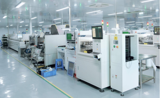
Automated Manufacturing Systems
Fully Automated Production Lines: The rise of automated manufacturing systems has greatly reduced the need for manual labor in PCB assembly. Robotic arms, pick-and-place machines, and automated soldering systems work together to assemble PCBs with minimal human intervention. This reduces the likelihood of human error, increases efficiency, and allows for 24/7 production.
Benefits of Automation: Automated systems are not only faster but also improve the consistency of each PCB assembly, ensuring that every board is built to the same exact standards. Furthermore, automation can handle more complex tasks, such as the placement of small and micro-components, which would be difficult for humans to manage manually.
Miniaturization of Components
Impact on PCB Design
Need for More Compact and Efficient Layouts: As electronic devices become smaller and more powerful, there is an increasing demand for miniaturized PCBs. This trend drives the need for more compact PCB designs that can accommodate smaller components without compromising functionality. Advanced design techniques, such as multi-layer PCBs and flexible PCBs, are becoming more common as manufacturers seek to fit more components into smaller spaces.
High-Density Interconnects (HDI): To achieve this, PCB designers are increasingly using HDI technology, which allows for tighter component placement and smaller traces on the board. This enables the production of high-performance devices, such as smartphones and wearables, that require smaller, yet more powerful, PCBs.
Challenges in Assembly
Handling Micro-Components: The miniaturization of components has created significant challenges in assembly. For example, placing micro-components with small footprints (such as 01005 resistors) on PCBs requires extreme precision. Specialized pick-and-place machines equipped with high-resolution cameras are used to handle these tiny components accurately.
Ensuring Precision Placement: With smaller components comes the risk of improper placement. Misalignment or soldering defects in micro-assemblies can result in functional issues, making precise alignment crucial. The use of advanced vision systems and AI-based inspection ensures that the placement is exact, and any errors are caught early in the process.
Green Manufacturing and Sustainability
Environmental Impact of PCB Assembly
Reducing Waste and Adopting Eco-Friendly Materials: As environmental concerns become more pressing, PCB manufacturers are focusing on green manufacturing practices. This includes efforts to reduce waste, improve energy efficiency, and adopt environmentally friendly materials in the PCB assembly process. For example, lead-free solder and halogen-free PCBs are becoming the industry standard as part of efforts to minimize harmful emissions and hazardous waste.
Closed-Loop Manufacturing: Some manufacturers are moving towards closed-loop manufacturing systems, where materials such as solder paste and PCB waste are recycled and reused, further reducing the environmental impact of PCB production.
RoHS and WEEE Compliance
RoHS Compliance: The Restriction of Hazardous Substances (RoHS) directive plays a significant role in shaping the future of PCB assembly. RoHS restricts the use of hazardous materials, such as lead, mercury, and cadmium, in the manufacturing of electronic products. This has led to the widespread adoption of lead-free soldering techniques and materials in PCB assembly.
WEEE Compliance: The Waste Electrical and Electronic Equipment (WEEE) directive requires manufacturers to ensure that electronic products are disposed of responsibly at the end of their lifecycle. This regulation is driving the development of more sustainable electronic waste recycling systems and the use of eco-friendly packaging to minimize environmental impact.
In conclusion, the future trends in PCB assembly are largely shaped by advancements in automation and AI, the drive for miniaturization in component design, and an increasing focus on sustainability. These trends are transforming the PCB assembly industry, improving production efficiency, enabling smaller, more powerful devices, and reducing the environmental footprint of manufacturing processes. As these technologies continue to evolve, the future of PCB assembly will likely feature even greater automation, higher precision, and more environmentally friendly practices.
Conclusion
In summary, PCB assembly is a complex, multi-step process that involves various techniques and rigorous testing to ensure the reliability and functionality of electronic products. From initial solder paste printing to final packaging, each stage plays a critical role in achieving high-quality results. As technology advances, methods like automated inspection, selective soldering, and lead-free soldering are becoming more integral to the industry, pushing the boundaries of precision and sustainability.
At PCBMASTER, we understand the importance of these processes and offer comprehensive solutions to meet the demands of modern electronics manufacturing. Whether you're looking for turnkey assembly or specialized testing services, we ensure every detail is handled with care, helping you deliver the best possible products to the market. With our expertise and commitment to quality, PCBMASTER stands ready to support your PCB assembly needs, from prototype to production.
FAQs
1. What is the difference between SMT and THT in PCB assembly?
SMT (Surface Mount Technology) and THT (Through-Hole Technology) are two methods used in PCB assembly to place components on a printed circuit board, each with its unique characteristics.
SMT (Surface Mount Technology) involves mounting components directly onto the surface of the PCB. It is more suitable for smaller, lighter components and is widely used for high-density boards. Advantages of SMT include smaller component sizes, faster production speeds, and higher automation capabilities. However, SMT may not be ideal for large, high-power components, as it offers less mechanical strength compared to THT.
THT (Through-Hole Technology), on the other hand, involves components with leads that pass through holes in the PCB and are soldered on the opposite side. THT is typically used for components that require strong mechanical bonds, such as connectors or high-power components. It is slower to assemble and takes up more space but offers greater durability and reliability in certain applications.
2. How does Automated Optical Inspection (AOI) improve PCB assembly quality?
Automated Optical Inspection (AOI) plays a crucial role in enhancing PCB assembly quality by providing an automated, high-precision method for inspecting solder joints, component placement, and overall board quality.
AOI uses high-resolution cameras to scan the surface of a PCB and compares the captured images with pre-programmed templates or reference designs. This process allows it to identify issues like soldering defects (cold joints, bridging, missing components), misplaced components, or dimensional discrepancies.
The advantages of AOI are its speed, consistency, and ability to detect small defects that could be missed by human inspectors. AOI helps ensure that only fully functional boards move to the next stage, preventing costly defects and improving overall assembly quality.
3. Why is lead-free soldering important, and what are its challenges?
Lead-free soldering has become a standard practice in PCB assembly due to increasing environmental concerns and regulations such as RoHS (Restriction of Hazardous Substances), which bans the use of lead in electronics manufacturing.
Why it’s important: Lead-free soldering reduces the environmental impact of electronic waste by eliminating the toxic effects of lead. It is also essential for ensuring compliance with global environmental standards and improving the safety of end users.
Challenges with lead-free soldering: The main challenge of lead-free soldering lies in its higher melting temperatures. Lead-free solders typically require temperatures between 217-221°C, compared to the 183°C needed for traditional lead-based solders. This difference in temperature can put more stress on components and PCB materials, potentially leading to thermal damage or solder joint reliability issues. Achieving consistent, high-quality solder joints with lead-free materials requires more precise control over the soldering process, making it more challenging than traditional methods.
4. What are the advantages of using In-Circuit Testing (ICT) over Functional Testing (FCT)?
In-Circuit Testing (ICT) and Functional Testing (FCT) are both used to ensure the quality and functionality of PCBs, but each has its strengths and limitations.
ICT focuses on testing individual components and the electrical integrity of the PCB, including solder joint quality, component placement, and continuity checks. It provides highly accurate diagnostics, detecting issues like open circuits, misplaced components, and parameter deviations. The main advantage of ICT is that it can quickly identify basic electrical faults before the board is subjected to more complex functional tests, saving time and reducing the risk of defects propagating to later stages.
FCT, on the other hand, tests the board's overall functionality under actual operating conditions. It ensures that the board performs as expected, such as checking whether a sensor outputs the correct signal or if a microcontroller executes its program correctly. While FCT is essential for verifying product usability, it does not catch the basic electrical issues that ICT detects. However, ICT cannot verify the full functionality of the device, making both tests complementary.
5. How does the rework process work in PCB assembly, and what tools are commonly used?
The rework process in PCB assembly is the corrective action taken to fix defects that arise during the assembly process. These defects may include misplaced components, cold solder joints, or soldering bridges.
Rework Steps:
1. Identifying defects: The first step in the rework process is identifying the defective areas on the PCB, which can be done through inspection (AOI) or testing (ICT/FCT).
2. Removing faulty components: Using hot air rework stations or soldering irons, faulty components are carefully removed.
3. Correcting the issue: The defective component is replaced, and new solder joints are created to restore the PCB to its proper condition.
Common Rework Tools:
Soldering Irons: Used for precise manual soldering to fix small components.
Hot Air Rework Stations: Provide heat to desolder components without damaging the PCB.
Laser Soldering Systems: Used for high-precision rework tasks, particularly with small or densely packed components.
Rework Challenges: One of the main challenges in rework is maintaining the integrity of sensitive components. Improper rework can cause further damage to the board, leading to more complex repairs. Hence, rework must be done with precision to ensure the PCB's functionality and reliability are not compromised.