


Single Layer Printed Circuit Board: Complete Guide for Beginners
Single layer printed circuit boards quietly power many of the devices we use every day, from remote controls to basic LED lights. Their simplicity makes them easy to understand and work with, while still offering enough functionality for a wide range of applications. Learning how these boards are designed, built, and used provides a solid foundation for anyone interested in electronics and hands-on projects.
Introduction to Single Layer Printed Circuit Boards
What is a Single Layer PCB?
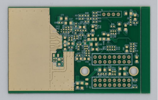
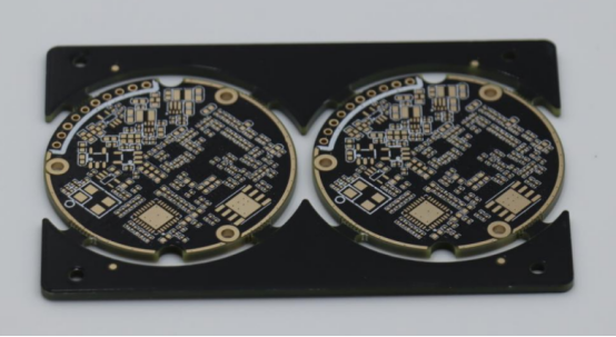
A single layer printed circuit board (PCB) is a type of PCB that has a single layer of conductive material, usually copper, on one side of the board, while the other side is used for mounting electronic components. The conductive layer forms a network of traces that connect components such as resistors, capacitors, and integrated circuits. The board is typically covered with a solder mask to protect the traces and a silkscreen layer for labeling components.
Compared to double-layer or multi-layer PCBs, single layer PCBs are simpler and easier to design. A double-layer PCB has conductive layers on both sides of the board, allowing for more complex routing, while multi-layer PCBs contain three or more layers, which are stacked to support highly complex or high-density circuits. This makes single layer PCBs ideal for basic electronic projects and low-cost devices, where complex wiring is not required.
Single layer PCBs are commonly found in everyday electronics, including remote controls, simple LED lights, calculators, power supplies, and small sensors. Their straightforward design makes them easy to repair and modify, which is particularly useful for beginners and small-scale manufacturers.
Importance in Electronics Industry
Single layer PCBs are valued in the electronics industry for several reasons. First, they are cost-effective for simple circuits, as they require less material and fewer manufacturing steps compared to multi-layer boards. This makes them ideal for products where high complexity is unnecessary.
Second, they are easy to manufacture and prototype. Their simple design allows for faster production, fewer errors during assembly, and lower testing requirements. Engineers and hobbyists can quickly move from schematic design to a working prototype without specialized equipment.
Many common electronic devices rely on single layer PCBs. Examples include remote controls, basic power supplies, LED lighting circuits, toys, and small household gadgets. These applications demonstrate how single layer PCBs balance functionality and cost, making them a practical choice for both mass production and DIY projects.
Components of a Single Layer PCB
Substrate Material
The substrate is the base layer of a single layer PCB, providing mechanical support for all other components. Common substrate materials include FR-4, CEM-1, and phenolic paper.
FR-4: Made of fiberglass epoxy, it offers excellent insulation, durability, and heat resistance, making it suitable for most industrial and commercial applications.
CEM-1: A composite material combining paper and epoxy, it is cheaper than FR-4 but less durable, often used in low-cost consumer electronics.
Phenolic paper: Made from paper reinforced with phenolic resin, it is very low-cost but has lower heat resistance and mechanical strength.
Material | Insulation | Durability | Heat Resistance | Typical Use |
|---|---|---|---|---|
FR-4 | High | High | High | Industrial, commercial PCB |
CEM-1 | Medium | Medium | Medium | Budget electronics |
Phenolic Paper | Low | Low | Low | Toys, small gadgets |
The choice of substrate affects the PCB’s thermal performance, mechanical strength, and overall reliability.
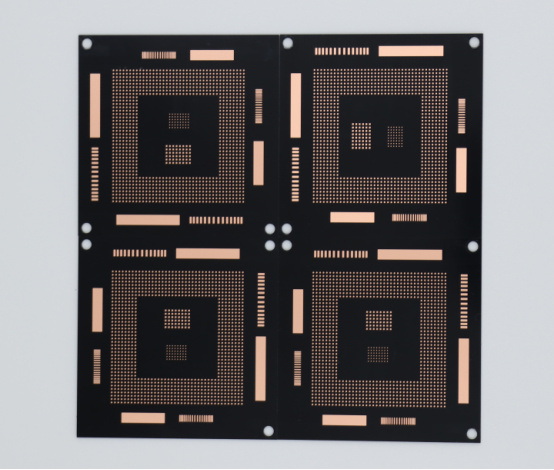
Conductive Layer
The conductive layer of a single layer PCB is usually made of copper, which forms the traces that carry electrical signals between components.
Copper thickness is measured in ounces per square foot (oz/ft²), typically ranging from 0.5 oz to 2 oz. Thicker copper can carry higher currents without overheating.
The role of copper traces is to provide reliable electrical connectivity while minimizing resistance and signal loss.
Visual examples: Copper traces can appear as thin lines connecting resistors, capacitors, and ICs, visible after etching and before applying the solder mask.
Correctly designing the conductive layer is essential for signal integrity, heat management, and overall PCB performance.
Solder Mask and Silkscreen
The solder mask is a protective coating applied over the conductive copper to prevent accidental shorts and corrosion. It is typically available in green, red, blue, black, and other colors, with green being the most common.
The silkscreen layer is printed on top of the solder mask and provides component labels, logos, or reference designators, helping with assembly and troubleshooting.
Step-by-step example of silkscreen application:
1. Apply the solder mask to the copper layer and cure it.
2. Prepare the silkscreen ink with the desired component markings.
3. Use a screen printing or inkjet process to print the markings onto the solder mask.
4. Cure the silkscreen layer to ensure durability during soldering.
Together, the solder mask and silkscreen protect the PCB, guide component placement, and improve readability, making assembly faster and reducing errors.
Design Principles for Single Layer PCBs
Layout and Schematic Design
The first step in designing a single layer PCB is translating a circuit schematic into a physical layout. A schematic shows the electrical connections between components, while the PCB layout defines the actual positions of components and the copper traces that connect them.
How to translate a schematic to a PCB layout:
1. Import the schematic into PCB design software.
2. Place components on the board according to their functional relationships.
3. Route the electrical connections with traces while avoiding overlaps and shorts.
4. Verify the design using software simulation or design rule checks (DRC).
Common software tools for single layer PCB design include Eagle, KiCad, and Altium. These tools offer features like automatic trace routing, component libraries, and layout validation, making it easier to create accurate and manufacturable designs.
Example: Designing a simple LED circuit:
Start with a schematic showing a power source, resistor, and LED.
Place the resistor close to the LED to minimize trace length.
Connect the components with copper traces following the schematic.
Verify correct polarity for the LED and ensure adequate spacing.
Trace Routing and Width
Trace routing is the process of drawing copper paths that connect components on the PCB. Proper routing ensures electrical performance and prevents short circuits.
Guidelines for trace width and spacing:
Wider traces can carry more current without overheating.
Maintain adequate spacing between traces to prevent shorts or signal interference.
Use design rules based on the board’s voltage and current requirements.
Calculating current-carrying capacity:
Formula: 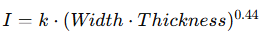 (simplified for small boards).
Use online calculators or software tools for precise values based on copper thickness and temperature rise.
Examples of correct vs. incorrect routing:
Correct: Traces follow a logical path, avoid unnecessary bends, maintain spacing, and keep signal traces short.
Incorrect: Traces overlap, take long detours, or pass too close to other components, causing interference or risk of shorts.
Component Placement
Proper component placement is essential for minimizing interference, simplifying assembly, and improving performance.
Best practices:
Place components in logical groups according to the circuit function.
Keep high-current components away from sensitive signal lines.
Align components along rows or grids for easier soldering and inspection.
Step-by-step example of placing components:
1. Start with the power source and critical components (e.g., voltage regulators).
2. Place resistors and capacitors close to the ICs they support.
3. Orient polarized components (like LEDs and diodes) consistently.
4. Leave enough clearance for heat dissipation and soldering tools.
5. Double-check connections and spacing before finalizing the layout.
Correct placement reduces noise, improves reliability, and makes the PCB easier to assemble and test.
Manufacturing Process of Single Layer PCBs
PCB Fabrication Steps
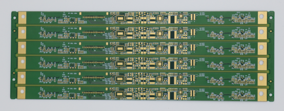
The manufacturing of a single layer PCB involves several key steps that transform a design into a functional circuit board. The main steps are designing, printing, etching, drilling, and plating.
Step-by-step flow of the process:
1. Designing: Create the PCB layout using CAD software, including component placement and trace routing.
2. Printing: Transfer the design onto a photoresist layer applied to the copper-clad substrate. This defines the areas to keep or remove.
3. Etching: Remove unwanted copper using a chemical solution, leaving only the desired copper traces.
4. Drilling: Drill holes for component leads and mounting points. Precision ensures proper alignment during assembly.
5. Plating: Apply a thin layer of metal to the holes and copper traces if needed, enhancing electrical conductivity and solderability.
Following this sequence ensures that the PCB is accurately produced according to the design and ready for assembly.
Surface Finishes and Coatings
After fabrication, PCBs often receive surface finishes to protect the copper and improve solderability. Common types include:
HASL (Hot Air Solder Leveling): Coats the copper with a layer of solder; cost-effective, suitable for standard applications, but less flat for fine-pitch components.
ENIG (Electroless Nickel Immersion Gold): Provides excellent durability and corrosion resistance; ideal for high-reliability or fine-pitch PCBs, but more expensive.
OSP (Organic Solderability Preservative): A thin protective layer that preserves copper for soldering; low cost and environmentally friendly, but shorter shelf life.
Finish | Durability | Cost | Typical Use |
|---|---|---|---|
HASL | Medium | Low | Standard consumer electronics |
ENIG | High | High | High-reliability, fine-pitch circuits |
OSP | Low | Low | Short-run, budget-friendly boards |
Selecting the right finish balances cost, longevity, and performance requirements.
Quality Control and Testing
Quality control ensures that each single layer PCB functions correctly and meets specifications. Common tests include:
Continuity Testing: Verifies that all electrical connections are complete.
Insulation Resistance Testing: Ensures there are no short circuits or leakage paths between traces.
Visual Inspection: Detects visible defects such as broken traces, misaligned components, or solder mask issues.
Example of detecting common defects:
Short circuits: Occur when two copper traces touch unintentionally; detected via continuity or automated optical inspection.
Broken traces: Can interrupt the circuit; identified using resistance measurements across the trace.
Regular testing during manufacturing prevents faulty PCBs from reaching assembly and ensures consistent reliability.
Applications of Single Layer PCBs
Consumer Electronics
Single layer PCBs are widely used in consumer electronics due to their simplicity, low cost, and reliability. Common devices include remote controls, calculators, and LED lights.
Single layer PCBs are ideal for these applications because they handle low-complexity circuits efficiently. Their design allows for easy assembly and repair, while keeping manufacturing costs low. For example, a remote control uses a single layer PCB to connect buttons, resistors, and an IC, providing all necessary functionality without the complexity of multi-layer boards.
Industrial Equipment
In industrial applications, single layer PCBs are often used for simple control circuits and low-power power supplies. They provide reliable performance where high-density or multi-layer routing is unnecessary.
Comparison with double-layer PCBs:
Single layer PCB: Suitable for basic control circuits, lower cost, faster production, easier troubleshooting.
Double-layer PCB: Required for more complex industrial systems with higher component density, multiple signal paths, or increased power handling.
For instance, a small motor controller for a conveyor belt may use a single layer PCB for simple logic circuits, while a larger PLC system would require a double-layer or multi-layer PCB.
Educational and DIY Projects
Single layer PCBs are excellent for learning electronics and hobby projects. Their straightforward design allows beginners to understand circuit layout, soldering, and testing.
Example project: Designing a small buzzer circuit:
1. Place a resistor, buzzer, and transistor on the PCB.
2. Connect the components using short, clear copper traces.
3. Test the circuit by applying power and verifying sound output.
These projects demonstrate how single layer PCBs make electronics accessible, offering hands-on experience without the complexity of multi-layer designs.
Advantages and Limitations
Advantages
Single layer PCBs offer several key advantages that make them ideal for certain applications.
Cost-efficient: Single layer PCBs are significantly cheaper to produce compared to multi-layer boards. Their simple design reduces both material and manufacturing costs, making them the perfect choice for low-complexity circuits.
Simple and reliable: With fewer layers and components, single layer PCBs are less prone to errors during assembly. Their simplicity makes them highly reliable, especially in basic electronics like remote controls and LED circuits.
Easy to repair and manufacture: The straightforward structure of single layer PCBs makes them easier to inspect, troubleshoot, and repair. If a trace is damaged or a component fails, it’s relatively simple to identify and fix the issue. Additionally, they require less specialized equipment for manufacturing, which speeds up production.
Visual example: In a simple LED circuit, a single layer PCB easily connects the LED, resistor, and power supply. If the circuit malfunctions, it’s easy to follow the path and pinpoint where the issue lies. This simplicity makes single layer PCBs a preferred choice in industries where cost and speed are critical.
Limitations
While single layer PCBs have many advantages, they also come with some limitations that may make them unsuitable for more complex applications.
Limited complexity and density: Single layer PCBs can only accommodate a certain level of complexity. Complex circuits requiring a high number of components or interconnections may not fit within the available space.
Not suitable for high-speed or high-power circuits: Single layer PCBs may not handle the signal integrity or power requirements of high-speed or high-power circuits. Multi-layer boards, with their ability to provide more routing layers and better heat dissipation, are typically needed for such applications.
Comparison table: Single Layer vs. Multi-Layer PCBs
Feature | Single Layer PCB | Multi-Layer PCB |
|---|---|---|
Complexity | Low | High |
Density | Low | High |
Power Handling | Low | High |
| Signal Integrity | Limited | Excellent |
| Cost | Low | High |
| Manufacturing Time | Short | Long |
For example, a single layer PCB might be ideal for a simple sensor circuit, but if you need to design a high-speed data processing board, a multi-layer PCB would be necessary to handle the complexity and ensure reliable performance.
Tips for Beginners
Choosing the Right Materials and Tools
When starting with single layer PCBs, choosing the right materials and tools is crucial for success. Here’s a breakdown of the essential components you’ll need:
Substrates: For beginners, FR-4 is the most common and versatile choice, offering a good balance between durability, heat resistance, and cost. It’s widely used in consumer electronics and is suitable for most basic projects.
Solder Types: Use lead-free solder for safety and compliance with modern standards. Sn99Cu1 solder is a popular option, offering good flow characteristics and reliability.
Tools: You’ll need basic tools like a soldering iron, wire cutters, and tweezers. For PCB design, free software like KiCad or Eagle is a great starting point.
Example: Many beginners start with PCB kits that include everything you need: FR-4 boards, components, and a soldering guide. These kits allow you to practice soldering and circuit assembly before moving on to more complex designs.
Avoiding Common Mistakes
As a beginner, it’s easy to make mistakes, but understanding the common pitfalls can help you avoid them:
Misrouting traces: Traces should connect components logically, without unnecessary bends or crossing. Ensure traces are wide enough for the current they’ll carry and leave space between them to prevent shorts.
Poor soldering: Make sure the solder joints are clean and not “cold” (dull, cracked) or “bridging” (shorting between pads).
Incorrect component placement: Double-check the orientation of polarized components like diodes and electrolytic capacitors. Use the silkscreen layer for accurate component placement.
Step-by-step troubleshooting guide:
1. Check the schematic: Ensure the circuit design matches the PCB layout.
2. Inspect traces: Look for broken or shorted traces with a magnifying tool.
3. Verify component placement: Ensure all components are correctly oriented and seated.
4. Test connections: Use a multimeter to check for continuity and correct placement of resistors, capacitors, etc.
By following these steps, you can quickly identify and fix common issues, ensuring your first projects are successful.
Learning Resources
As you progress in PCB design and assembly, there are many resources available to help you improve your skills:
Online courses: Platforms like Udemy, Coursera, and LinkedIn Learning offer great beginner courses on PCB design, soldering, and electronics.
Tutorials and books: Websites like Instructables and Hackster.io provide step-by-step guides on a variety of projects, from simple circuits to more complex designs.
YouTube tutorials: Channels like Paul McWhorter or GreatScott! offer excellent tutorials on electronics and PCB design, breaking down complex topics into digestible lessons.
Example: A beginner might start with a YouTube tutorial on soldering and then move on to building their first PCB circuit with a kit or online tutorial. This practical experience, combined with the right resources, will help accelerate your learning.
Conclusion
Single layer PCBs are a great starting point for anyone looking to dive into the world of electronics. From the simple process of designing and manufacturing to their wide range of applications, these boards offer a solid foundation for both beginners and experienced hobbyists. By starting with small projects, you’ll gain valuable hands-on experience that will build your confidence and skills.
As you grow more comfortable with single layer PCBs, the next logical step is to explore double-layer and multi-layer PCBs. These more advanced designs open up new possibilities for handling complex circuits and higher component densities. Whether you're a beginner, hobbyist, or aiming to become a professional PCB designer, there’s always more to learn and explore in the world of PCBs.
If you have any further questions or want to dive deeper into PCB design, feel free to reach out to PCBMASTER. As an experienced PCB supplier, we can provide you with expert guidance and tailored solutions for your projects.
FAQs
What is the difference between single layer and double layer PCBs?
A single layer PCB has one conductive copper layer, which connects components and provides electrical paths. It is simple, cost-effective, and ideal for low-complexity circuits. In contrast, a double layer PCB has two conductive layers—one on each side of the board—allowing for more complex routing and higher component density. Double-layer PCBs are suitable for more intricate designs that require additional space for connections.
Can single layer PCBs handle high-power applications?
Single layer PCBs are generally not suitable for high-power applications. While they can handle low-power circuits, they may struggle with high current or power dissipation due to their limited copper thickness and lack of layers for better heat distribution. For high-power circuits, multi-layer PCBs are preferred, as they can manage higher currents and provide better heat management.
What are the common materials used for single layer PCBs?
The most common materials for single layer PCBs include:
FR-4: A fiberglass-based material, offering a good balance of insulation, heat resistance, and durability.
CEM-1: A composite material made from paper and epoxy resin, cheaper than FR-4, but less durable.
Phenolic paper: A low-cost, low-performance material, often used in consumer-grade devices like toys and basic gadgets.
These materials are selected based on cost, durability, and the specific application requirements.
How do I test a single layer PCB for faults?
To test a single layer PCB for faults, follow these steps:
1. Continuity Testing: Use a multimeter to check that all electrical connections are intact and that there are no broken traces.
2. Insulation Resistance Testing: Test for shorts between traces, ensuring there are no unwanted connections that could cause malfunction.
3. Visual Inspection: Inspect the PCB under good lighting to identify damaged traces, misaligned components, or soldering issues.
4. Component Testing: Check components like resistors and capacitors to ensure they are correctly placed and functioning.
Is designing a single layer PCB suitable for beginners in electronics?
Yes, designing a single layer PCB is ideal for beginners. It provides a straightforward introduction to PCB layout, component placement, and soldering. Single layer PCBs are easier to design, manufacture, and troubleshoot, making them an excellent choice for people just starting with electronics projects. As you gain confidence, you can move on to more complex designs, like double-layer or multi-layer PCBs.

