


Understanding PCBs in IoT Devices: How They Enable Smart, Connected Technology
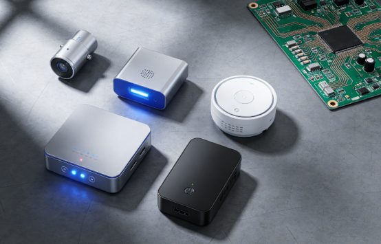
Printed Circuit Boards (PCBs) play a crucial role in making Internet of Things (IoT) devices function effectively. They connect and power the various parts of a device, such as sensors, microcontrollers, antennas, and batteries, enabling devices like smartwatches, home automation systems, and industrial sensors to work seamlessly.
IoT devices face three major challenges: they must be small, energy-efficient, and capable of maintaining strong wireless connections. This means that PCBs need to be compact, designed to use minimal power, and capable of ensuring reliable communication between all components. Through careful design, PCBs fit complex systems into small spaces, reduce energy consumption, and support various wireless protocols like Wi-Fi and Bluetooth.
In essence, PCBs are vital for building IoT devices that are efficient, reliable, and compact, meeting the demanding needs of the modern, connected world.
What Is a PCB in IoT? Definition and Core Structure
A PCB in IoT devices is a small, flat board that connects and holds all the essential components of a smart device. It helps the device work by directing signals, managing power, and enabling communication between different parts, such as sensors and wireless modules.
What makes PCBs in IoT different from traditional PCBs?
IoT PCBs are specifically designed to meet the unique needs of IoT devices. Unlike traditional PCBs used in desktop computers, IoT PCBs must be small, energy-efficient, and capable of supporting wireless communication. For example, while a regular PCB may have room for large components, an IoT PCB has to fit compact parts and make the most of limited space. It also must use very little power to extend battery life, often running on low energy to ensure that devices like smartwatches or sensors can last for long periods.
Typical materials used in IoT PCBs
IoT PCBs often use materials that balance performance, durability, and flexibility.
FR-4 is the most common material and provides a strong foundation for many devices.
Polyimide is used in flexible PCBs, allowing the board to bend without breaking, ideal for wearables or devices with irregular shapes.
PTFE (Teflon) is used for high-frequency applications where signal quality is essential, such as in medical IoT devices or those requiring fast data transfer.
Key Components of an IoT PCB
The key components of an IoT PCB include microcontrollers, sensors, wireless modules, and power management ICs.
Microcontroller (MCU): The brain of the IoT device. It processes data from sensors, controls the device's functions, and manages communication.
Sensors: These components collect data from the environment, like temperature, motion, or light. They send this data to the MCU for processing.
Wireless Modules: These allow the device to connect to networks, either via Wi-Fi, Bluetooth, or other protocols like LoRa (Long Range).
Power Management ICs (PMIC): These regulate the power supplied to the components, ensuring efficient battery usage and preventing overcharging.
Other important components include antennas, which allow wireless communication, and passive components like resistors and capacitors, which help stabilize power, filter signals, and maintain the overall stability of the system.
How PCBs Enable Sensor Integration and Data Flow
PCBs play a crucial role in connecting and organizing all the components in an IoT device. They create paths for signals by routing the necessary traces between components, allowing data to flow from the sensors to the microcontroller and from the microcontroller to other components like wireless modules.
For efficient data flow, PCBs must be designed with low-resistance pathways. This ensures that the signal travels quickly and accurately without losing power or causing delays. For example, in a fitness tracker, the PCB ensures that data from the heart rate sensor travels directly to the microcontroller for processing and then transmits it to the user’s smartphone via Bluetooth.
By ensuring minimal resistance and proper signal routing, PCBs help IoT devices work reliably, process data in real-time, and communicate with other devices or networks, ensuring seamless operation.
Why Do IoT PCBs Need Specialized Designs?
IoT devices have specific requirements that regular PCBs cannot meet. These devices need to be small, efficient, and capable of connecting wirelessly, which calls for specialized PCB designs. In this section, we’ll explore the different types of PCBs used in IoT and how specialized designs contribute to their performance.
What are the different types of PCBs used in IoT?
There are several types of PCBs designed specifically for IoT devices, each with unique features that meet different needs:
HDI (High-Density Interconnect) PCBs
HDI PCBs are ideal for miniaturized devices where space is limited. They use microvias (tiny holes) and fine-pitch traces to place more components in smaller areas. These PCBs allow designers to create complex, multi-layered boards while keeping the device compact. For example, smartwatches and tiny medical sensors rely on HDI technology to pack multiple components into small spaces.
Flexible PCBs
Flexible PCBs are made from materials like polyimide, which allows the board to bend and twist without breaking. This flexibility is essential for devices like wearables (e.g., fitness trackers and smartwatches) or devices with unconventional shapes. These PCBs can conform to the curves of a user’s wrist or fit into spaces that rigid boards cannot. Flexibility also makes them ideal for foldable devices like smartphone sensors.
Rigid-Flex PCBs
Rigid-flex PCBs combine both rigid and flexible sections in one board. The rigid parts hold components like microcontrollers, while the flexible parts allow the PCB to bend and adapt to different shapes. This design is crucial for devices that need both durability and flexibility, such as industrial sensors or smart glasses. Rigid-flex PCBs provide the strength of a rigid PCB with the adaptability of a flexible one.
How do specialized designs contribute to performance?
Specialized PCB designs directly impact how well an IoT device functions. The challenge is to make the device compact, energy-efficient, and able to communicate reliably, all while maintaining performance.
Miniaturization without Sacrificing Performance
One of the biggest challenges in designing IoT devices is making them small without losing performance. HDI PCBs tackle this by packing more components into a smaller space, using advanced techniques like microvias and fine-pitch components. This allows IoT devices like wearables to remain small and lightweight while still offering powerful performance.
Flexibility and Rigidity Impact IoT Applications
The choice between flexibility and rigidity in a PCB design can significantly affect the device’s performance and usability:
Flexible PCBs are critical for wearable devices like smartwatches, which need to bend with the user’s wrist. This flexibility ensures the device fits comfortably and moves with the wearer while still functioning perfectly.
Rigid-Flex PCBs are often used in industrial sensors that need to be durable and reliable but also flexible enough to fit in unique spaces. These devices might be placed in machines that vibrate or environments that require both strength and adaptability.
For example, a fitness tracker uses a flexible PCB to ensure the device stays close to the wrist, maintaining proper sensor readings without compromising comfort. In contrast, a smart thermostat uses a rigid-flex PCB, where the rigid sections hold the microcontroller and the flexible parts bend to fit within the device’s curved shape.
How Do PCBs Support IoT Connectivity and Signal Integrity?
Connectivity is one of the most important features of IoT devices. Without the ability to wirelessly connect to networks or other devices, IoT gadgets would not be able to perform their key functions, like sending data or receiving updates. In this section, we’ll look at how PCBs ensure stable wireless communication and maintain the integrity of signals within IoT devices.
Why is connectivity crucial for IoT devices?
Connectivity is essential for IoT devices because they rely on communication to work effectively. Whether it’s a smart thermostat adjusting the temperature based on data from your phone, or a wearable sending fitness data to an app, these devices need to stay connected to perform their tasks. The most common wireless technologies used in IoT devices are Wi-Fi, Bluetooth, and LoRa (Long Range). For these connections to work smoothly, the signals must be stable and strong, which depends heavily on the PCB design.
How does PCB design affect wireless performance?
PCBs play a critical role in the quality of wireless performance in IoT devices. The design of the PCB directly impacts how well signals are routed and transmitted through the device, which affects the device’s ability to maintain a stable connection.
Signal Routing: Minimizing Signal Loss and Interference
A well-designed PCB routes signals carefully to avoid interference and signal loss. Sharp bends or poorly placed traces can cause signal reflections, leading to weaker connections and slower data transmission. For example, in a smart speaker, the PCB is designed with precise routing to ensure that signals from the microphone, microcontroller, and Wi-Fi module flow smoothly with minimal loss, so the device can recognize your voice and send data to the cloud without delays.
The Role of Impedance-Controlled Traces and Ground Planes
Impedance-controlled traces and ground planes are key design elements in maintaining signal integrity. Impedance-controlled traces ensure that the electrical signals travel along a stable path, reducing the risk of signal degradation. This is especially important for high-speed signals like Wi-Fi and Bluetooth, where even small changes in the signal path can lead to poor performance.
Ground planes are used to shield sensitive components, like antennas and wireless modules, from interference caused by nearby circuitry. By placing a ground plane underneath the antenna traces, designers can block unwanted noise, ensuring that wireless signals remain strong and clear.
Case Study: Smart Home Devices and Their PCB Connectivity
To better understand how PCBs support IoT connectivity, let’s look at the example of a smart thermostat.
How a Smart Thermostat PCB Ensures Reliable Communication with the Phone
A smart thermostat relies on its PCB to ensure that it communicates reliably with your smartphone. The PCB in a smart thermostat connects the temperature sensors, microcontroller (MCU), Wi-Fi module, and antenna. The design of this PCB ensures that data can flow smoothly from the sensors to the MCU, which then sends the data to the Wi-Fi module.
The Wi-Fi module transmits the data to your phone, allowing you to adjust the temperature remotely. The PCB ensures that all components are connected properly, and its design minimizes interference. The use of impedance-controlled traces and ground planes helps maintain strong signal strength, preventing interruptions in communication, even when the thermostat is placed inside a wall or far from the Wi-Fi router.
What Role Does Power Management Play in IoT PCB Design?
In IoT devices, power management is crucial because many of these devices run on batteries and need to conserve energy to function for long periods. PCBs play an essential role in ensuring that the device uses power efficiently, extending battery life, and preventing unnecessary energy waste. This section will explore how PCB design impacts energy consumption, the role of Power Management ICs (PMICs), and how efficient power management is critical for wearable devices.
How does PCB design impact energy consumption?
PCB design directly influences how efficiently an IoT device uses power. Properly designed PCBs reduce energy consumption by ensuring that the components get the right amount of power without wasting any.
Power-efficient routing: Reducing resistance and energy waste
In a PCB, power-efficient routing involves designing traces (the paths that electrical signals follow) that minimize resistance. Resistance in the PCB traces causes energy to be wasted as heat. By using thicker copper traces and optimizing the layout, the resistance can be lowered, which helps reduce energy loss. This is especially important for low-power IoT devices like sensors or wearables, where conserving every bit of energy is crucial for longer battery life.
Using power gating and low-power components to extend battery life
Power gating is a technique used in IoT PCBs to turn off certain components when they are not in use. For example, a motion sensor in a smart home device might only need to be active when it detects movement. By power gating the sensor when it’s idle, the PCB saves power and extends the device’s battery life. Additionally, low-power components, such as low-voltage microcontrollers and sensors, are used in IoT designs to further reduce energy consumption. These components are designed to operate efficiently at very low power levels, allowing devices like fitness trackers to last for days or even weeks on a single charge.
The Importance of Power Management ICs (PMICs)
Power Management ICs (PMICs) are specialized chips on the PCB that handle the distribution of power to various components. They ensure that each part of the device receives the correct voltage and current, which helps optimize energy usage.
Regulating voltage for different IoT components
In IoT devices, different components require different voltage levels. For example, the microcontroller (MCU) may need 3.3V, while a sensor might require only 1.8V. A PMIC regulates and converts the battery voltage to the appropriate levels for each component. This regulation is important because it prevents components from being over- or underpowered, ensuring both performance and energy efficiency. Without a PMIC, each component would need its own power regulator, leading to increased complexity and energy waste.
Case Study: Wearable Devices and Power Efficiency
Wearable devices, such as smartwatches and fitness trackers, are a great example of how power management is crucial in IoT devices.
Example: Smartwatch PCBs using power management to last longer on a single charge
Smartwatches have limited space for both their battery and their PCBs, so managing energy efficiently is essential. The PCB in a smartwatch uses several power-saving techniques, including:
Power-efficient routing: The PCB layout ensures that traces are as short and thick as possible to reduce resistance and minimize energy loss.
Power gating: Components like the heart rate sensor or display are turned off when not in use. For instance, the display may go dark when the watch is idle, saving power.
Low-power components: Smartwatches use low-power MCUs and sensors that consume very little energy, allowing the device to last for several days on a single charge.
Through these techniques, smartwatches can offer impressive battery life despite having a small battery. This careful power management makes wearables practical for daily use without frequent charging.
What Are the Challenges in PCB Design for IoT Devices?
Designing PCBs for IoT devices presents unique challenges that go beyond traditional electronic devices. These challenges arise due to the compact size, energy efficiency, durability, and environmental factors that IoT devices need to handle. In this section, we'll explore the main challenges IoT PCB designers face, including miniaturization, durability, and the environmental factors that affect the design.
What are the key challenges when designing IoT PCBs?
Designing IoT PCBs requires addressing several challenges to ensure that the device functions effectively, efficiently, and reliably. Two of the primary challenges are miniaturization and durability.
Miniaturization: Balancing Space Constraints with Performance
Miniaturization is one of the most significant challenges in IoT PCB design. Many IoT devices, like smartwatches or wearable fitness trackers, must be small and compact. The limited space makes it difficult to fit all the necessary components (like sensors, microcontrollers, and wireless modules) without compromising performance. To overcome this challenge, designers use High-Density Interconnect (HDI) technology, which allows them to place more components in a smaller area. By using microvias and fine-pitch components, designers can ensure that the device remains small without sacrificing functionality.
Durability: Ensuring Long-lasting Operation in Harsh Environments
Another challenge in IoT PCB design is ensuring that the device can withstand harsh environments. Many IoT devices, especially those used in industrial settings, need to be durable and capable of operating under tough conditions. This means the PCB must be resistant to vibration, moisture, and extreme temperatures. To address these challenges, designers use materials that are both robust and flexible, such as polyimide (for flexible devices) or FR-4 (a durable, cost-effective option). They may also use conformal coatings to protect the board from environmental damage and heavy copper layers for extra durability.
How do IoT devices face unique environmental challenges?
IoT devices are often used in unpredictable and harsh environments, making environmental resistance a key factor in their design. These devices must be able to handle various physical stressors like moisture, dust, vibration, and temperature extremes.
Resistance to Moisture, Dust, Vibration, and Temperature Extremes
Many IoT devices, particularly in Industrial IoT (IIoT) or outdoor sensors, are exposed to extreme conditions. Devices like smart home sensors, weather stations, or wearable devices may encounter moisture, dust, and temperature fluctuations. To protect the PCB, designers apply conformal coatings (e.g., silicone or acrylic coatings) that shield the board from water, dust, and physical wear. These coatings also provide a protective barrier against environmental elements like dirt, rain, or chemicals, which is especially important for devices used outdoors or in industrial settings.
Vibration is another concern in environments like factories or vehicles, where PCBs can be exposed to constant movement. In these cases, the PCB must be designed to resist physical stress without losing functionality. Using flexible PCBs or rugged coatings ensures that the board can survive such environments.
Designing for Longevity in Industrial IoT (IIoT)
In Industrial IoT (IIoT) applications, longevity is a critical factor. Many of these devices are designed to operate for several years in demanding conditions, requiring rugged and durable PCB designs.
How rugged PCB materials and coatings help IoT devices perform over long periods
For Industrial IoT (IIoT) devices, ruggedization is essential to ensure the device works reliably for many years, even in extreme environments. For example, automotive sensors, oil rig equipment, or factory machinery sensors are exposed to intense heat, cold, and moisture. Using high-quality materials like FR-4, polyimide, or PTFE helps ensure the PCB remains operational under these conditions. Heavy copper traces are often used to handle high currents, while thick PCB layers add strength and resistance to physical wear. Additionally, conformal coatings or epoxy resins protect the board from moisture, dust, and corrosion, helping to prolong the lifespan of the device.
To enhance longevity further, thermal management is vital. Thermal vias (small holes in the PCB that conduct heat away from components) and copper pours (large areas of copper) help dissipate heat from components like microcontrollers and power management ICs (PMICs). Proper heat management is essential to prevent overheating, which can shorten the device's lifespan.
How Do IoT PCBs Enable Real-Time Data Processing and Communication?
In the world of IoT devices, data is the lifeblood that powers decisions and actions. Whether it's tracking your fitness, controlling smart home devices, or monitoring industrial machinery, IoT devices rely on real-time data processing to operate efficiently. PCBs play a vital role in ensuring that this data flows quickly, accurately, and seamlessly between the various components of IoT systems. This section will explain how PCBs help IoT devices handle data processing and communication in real-time.
Why is Data Processing Critical in IoT Devices?
Data processing is a crucial function in IoT devices because it allows these devices to make decisions based on the data they collect. In real-time applications, such as predictive maintenance in factories or health monitoring in wearables, devices need to process and respond to data without delay.
The Importance of Fast, Accurate Data Handling for Real-Time IoT Applications
IoT devices must be able to handle data swiftly and accurately to provide real-time insights. For example, a predictive maintenance system in a factory relies on sensors that monitor machines' temperature, vibration, and pressure. When these sensors detect an issue, the device must quickly process the data and send alerts before a failure occurs. If the data processing is slow or inaccurate, it could lead to machine breakdowns or missed opportunities for early repairs, resulting in costly downtime. PCBs are essential for ensuring that these systems can process data efficiently and with minimal delay.
How Do PCBs Facilitate High-Speed Data Transfer?
In many IoT applications, devices need to transfer large amounts of data quickly and reliably. PCBs enable this by providing the signal pathways that connect the different components of an IoT device, like sensors, microcontrollers, and communication modules. The design and materials used in PCBs play a significant role in data transfer speed and signal integrity.
Using Materials Like PTFE for High-Frequency Signals and Fast Communication
To ensure fast communication between components, high-frequency signals need to travel through the PCB without losing strength or quality. Materials like PTFE (Polytetrafluoroethylene) are commonly used in high-speed PCBs because they have excellent dielectric properties, meaning they allow signals to pass through with minimal signal loss or interference. This is particularly important for IoT devices that rely on Wi-Fi, Bluetooth, or 5G to communicate, where fast data transfer is essential for real-time operation. For example, in smart home systems, data from motion sensors or temperature sensors must be transmitted almost instantaneously to the cloud or a central controller for immediate action.
The Role of PCB Design in Signal Integrity
In addition to using the right materials, PCB design also plays a crucial role in ensuring that signals are transmitted without distortion. Impedance-controlled traces and ground planes are essential design features that ensure stable signal paths for high-speed data. Ground planes are metal layers beneath the PCB’s surface that prevent signal interference by blocking unwanted noise from other components. Signal traces, which are the paths through which electrical signals flow, must be routed carefully to avoid sharp bends that could cause signal reflections or data loss. Together, these features ensure that data is transmitted cleanly and without delay, crucial for applications like remote patient monitoring or smart grid systems, where real-time communication is necessary for system performance.
Case Study: Industrial IoT Controllers and Data Flow
IoT devices are transforming industries, especially in sectors like manufacturing, energy, and logistics. In these industries, real-time data processing is vital for ensuring that equipment runs smoothly and efficiently. One key area where PCBs play an essential role is in industrial IoT controllers—devices that collect, process, and send data from sensors to a central system for analysis.
Example: A PCB’s Role in an Industrial Controller Processing Real-Time Sensor Data
Let’s look at an industrial IoT controller used in a manufacturing plant. This controller may collect data from temperature sensors, pressure sensors, motion detectors, and vibration sensors spread across different machines on the factory floor. The PCB within the controller connects all these sensors to the microcontroller (MCU), which processes the data. After processing, the controller sends the data to a central system, where it’s analyzed to predict potential failures or optimize operations.
The PCB is designed to handle high-speed data transfer between these components, ensuring that the system can react quickly to changes in sensor readings. For example, if a machine shows signs of overheating, the controller may trigger an alert or automatically shut down the machine to prevent damage. The use of high-quality materials like PTFE for signal integrity, coupled with careful PCB layout design, ensures that the data from all the sensors is transmitted without error or delay, even in an industrial environment where there may be high levels of electromagnetic interference.
What Are the Key Design Principles for Effective IoT PCB Design?
Designing a PCB for an IoT device requires careful consideration of several critical factors to ensure that the device operates efficiently, reliably, and is compact enough for modern applications. Below, we explore the most important design principles for IoT PCBs, including miniaturization, surface-mount technology (SMT), multilayer designs, and flexibility and ruggedness in various IoT applications.
Miniaturization Techniques for IoT PCBs
Miniaturization is essential for IoT devices because these devices must fit into small enclosures while maintaining performance. The smaller the PCB, the less power it consumes, and the more portable the device becomes. Three key miniaturization techniques used in IoT PCB design are HDI technology, 3D PCB printing, and embedded components.
HDI Technology (High-Density Interconnect)
HDI PCBs are designed with microvias (tiny holes) and fine-pitch components to pack more features into a small space. This allows for the integration of multiple components, like microcontrollers, sensors, and wireless modules, into a compact board. HDI technology is crucial for IoT wearables and miniature devices that need to be as small as possible without sacrificing functionality.
3D PCB Printing
3D PCB printing enables the creation of three-dimensional circuit boards, allowing the designer to build more complex shapes that fit specific enclosures, like those in wearable devices or smart glasses. This technique helps in utilizing vertical space and reduces the need for additional layers, improving both space efficiency and performance.
Embedded Components
Embedded components are those that are integrated directly into the PCB rather than being placed on the surface. This approach saves valuable space on the PCB surface and helps make the device more compact and functional. For example, resistors, capacitors, and even microcontrollers can be embedded within the PCB to reduce the overall board size without compromising performance.
The Importance of SMT and Multilayer Designs
To optimize performance and durability, IoT PCBs often incorporate Surface Mount Technology (SMT) and multilayer designs.
Why Surface-Mount Technology (SMT) is Essential
SMT allows components to be mounted directly onto the surface of the PCB, rather than through holes. This results in a more compact design and allows for components to be placed on both sides of the PCB, maximizing the available space. Additionally, SMT components are more durable, as they are soldered directly onto the PCB, which reduces the risk of mechanical failure compared to traditional through-hole components.
Multilayer Designs for Increased Space and Performance
Multilayer PCBs are made by stacking several layers of material to create multiple routing paths for signals and power. This enables IoT devices to have more components and features without increasing the board's size. Multilayer designs improve signal integrity, allow for better power distribution, and can even help to reduce electromagnetic interference (EMI). For example, a 6-layer PCB might have separate layers dedicated to power planes, ground planes, and signal routing, enhancing the overall performance of the device.
Designing for Flexibility and Ruggedness in Wearables and Industrial IoT
Wearables and Industrial IoT (IIoT) devices often face unique challenges due to their environments and design requirements. Flexible and rugged PCBs are essential for ensuring that these devices function reliably under difficult conditions.
How Flexible and Rigid-Flex Designs Allow for Unique Enclosures
Flexible PCBs are made from materials like polyimide that can bend and twist without breaking. This makes them ideal for wearable devices like smartwatches and fitness trackers that need to conform to the shape of the human body. A rigid-flex PCB, which combines both rigid and flexible sections, allows for a mix of durability in some areas (e.g., microcontrollers or batteries) and flexibility in others (e.g., sensors or antennas). This combination allows devices to maintain their performance while fitting into complex, curved enclosures.
Designing for Ruggedness in Industrial IoT (IIoT)
Industrial devices, such as those used in factories or outdoor environments, must withstand harsh conditions like extreme temperatures, moisture, dust, and vibration. To ensure long-lasting performance, IIoT PCBs use rugged materials like FR-4 (for temperature and moisture resistance) or polyimide (for flexibility in wearables). Protective coatings like silicone or acrylic can be applied to IIoT PCBs to protect them from environmental factors. Additionally, thick copper layers help dissipate heat and improve the thermal management of industrial devices, ensuring that the PCB remains stable even in extreme conditions.
Conclusion
To wrap up, PCBs are essential for the performance and functionality of IoT devices. They enable key features like connectivity, energy efficiency, and the seamless integration of sensors, processors, and wireless modules. Specialized PCB designs are crucial for meeting the specific needs of IoT devices, such as miniaturization, low power usage, and signal reliability. As IoT devices continue to advance, so too will the role of PCBs, with innovations in materials, 3D printing, and AI-assisted design leading to even smaller, more powerful, and efficient devices.
With extensive experience in the field, PCBMASTER stands out as a trusted supplier, offering top-quality PCBs for various industries, particularly IoT. Our expertise ensures that businesses receive reliable, durable, and cutting-edge PCB solutions, helping them stay ahead in the fast-evolving world of IoT technology.
FAQs
1. What is the main function of a PCB in IoT devices?
The main function of a PCB in IoT devices is to connect all the essential components of the device, such as sensors, microcontrollers (MCUs), antennas, and power management circuits. It ensures that these components can communicate with one another and perform their individual functions. For example, a sensor collects data (like temperature or motion), which is then processed by the MCU. The PCB routes signals between these components, ensuring that the data is transferred efficiently. It also helps with power distribution, making sure each component receives the appropriate voltage to operate effectively. Without a properly designed PCB, IoT devices would not function properly, as all components rely on the PCB to interact, share data, and remain powered.
2. How does a PCB affect the battery life of IoT devices?
A well-designed PCB significantly influences the battery life of IoT devices by minimizing energy loss and ensuring efficient power distribution. IoT devices, especially battery-powered ones, must operate for extended periods on a single charge, which requires careful attention to power consumption. PCBs achieve this by using efficient power routing — this means that the pathways for electrical current are carefully planned to avoid unnecessary resistance, which can lead to energy loss. Additionally, low-power components like microcontrollers (MCUs) and power management ICs are integrated into the PCB design to reduce the overall power draw. Power gating techniques, where power is only supplied to components when needed, also extend battery life. By using thick copper traces to reduce heat and fine-pitch traces to minimize space, a good PCB design ensures that energy is conserved and used efficiently, allowing IoT devices to last longer on a single battery charge.
3. What’s the difference between HDI and standard PCBs in IoT?
HDI (High-Density Interconnect) PCBs are designed for IoT devices that require high levels of miniaturization and performance in a small form factor. The key difference between HDI PCBs and standard PCBs lies in the construction and density of the traces and vias. HDI PCBs use microvias (very small holes) and fine-pitch traces, allowing more components to fit in a smaller space. This makes HDI PCBs ideal for devices like smartwatches, wearables, and miniaturized sensors, where space is limited. On the other hand, standard PCBs are typically larger, have fewer layers, and use through-hole vias (larger holes), which make them less suitable for small, compact IoT devices. In short, HDI PCBs are essential when you need to fit more features into a small, space-constrained device, while standard PCBs are used for less compact designs.
4. Why are flexible PCBs important in IoT?
Flexible PCBs are crucial in IoT applications, particularly for wearables and devices with unconventional shapes. These PCBs are made from flexible materials like polyimide, which allow them to bend, fold, and twist without breaking. This flexibility is particularly important for devices like smartwatches, fitness trackers, and health-monitoring wearables, where the PCB needs to conform to curved surfaces or fit into a small, compact design. Flexible PCBs provide design versatility by allowing IoT devices to be placed in environments where traditional rigid PCBs wouldn't fit. They also allow for lighter, more durable devices that can withstand constant bending without damage, making them more reliable in long-term use. For instance, a flexible PCB in a fitness tracker allows the device to wrap around the wrist comfortably, maintaining connectivity while being durable and compact.
5. Can IoT PCBs be repaired if damaged?
Repairing IoT PCBs is challenging because most of these devices use surface-mount technology (SMT), where components are soldered directly onto the surface of the board rather than through holes. This makes the components smaller and the PCB more compact but also harder to repair or replace. If a component fails, it is often difficult to replace it without special equipment and expertise. However, modular PCB designs have become a solution in some IoT devices. In these designs, the components are organized into modular sections, so rather than replacing the entire board, only the damaged module (like a sensor or wireless module) needs to be replaced. For example, in industrial IoT devices, sensors that connect to a main controller via the PCB might be replaceable individually, reducing the need for a full board replacement. While not all IoT PCBs are repairable, modular designs offer a pathway for cost-effective repairs without discarding the entire device.
Author Bio
Hi, I'm Carol, the Overseas Marketing Manager at PCBMASTER, where I focus on expanding international markets and researching PCB and PCBA solutions. Since 2020, I've been deeply involved in helping our company collaborate with global clients, addressing their technical and production needs in the PCB and PCBA sectors. Over these years, I've gained extensive experience and developed a deeper understanding of industry trends, challenges, and technological innovations.
Outside of work, I'm passionate about writing and enjoy sharing industry insights, market developments, and practical tips through my blog. I hope my posts can help you better understand the PCB and PCBA industries and maybe even offer some valuable takeaways. Of course, if you have any thoughts or questions, feel free to leave a comment below—I'd love to hear from you and discuss further!

