


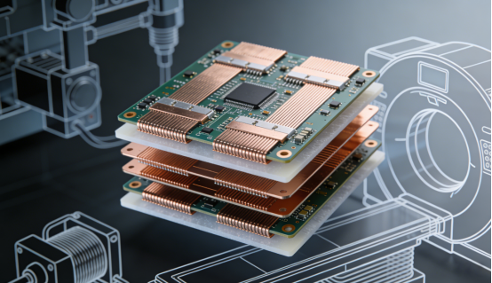
How Multi-Layer PCBs Solve Withstand Voltage Challenges for High-Voltage Applications
Multi-layer PCBs (Printed Circuit Boards) are essential components in many high-voltage electronic devices, from industrial power supplies to medical imaging machines. These PCBs stack multiple copper layers, which allow for more complex circuits in a smaller space, but they also face a critical challenge: ensuring reliable insulation between layers to prevent electrical breakdown. In high-voltage applications, any insulation failure can lead to dangerous issues such as short circuits, arcing, or even fires, making it crucial to address these risks in the design and manufacturing process.
This guide will explore how multi-layer PCBs overcome these challenges through careful material selection, precise design, and advanced manufacturing techniques. By focusing on key strategies such as using high-performance dielectric materials, controlling insulation thickness, and conducting rigorous testing, this article aims to provide a clear understanding of how multi-layer PCBs maintain safety and reliability in high-voltage environments. Whether you're designing for industrial, medical, or automotive applications, understanding these strategies is key to ensuring your PCBs perform safely under high voltage stress.
What Is Withstand Voltage and Why Is It Critical for Multi-Layer PCBs?
Definition of Withstand Voltage
Withstand voltage refers to the maximum electrical voltage that a PCB can handle without breaking down. This breakdown happens when the electrical pressure exceeds the material’s ability to resist, causing current to leak or jump between layers. The material that separates copper layers on a PCB is called a dielectric, and its strength is critical. If the dielectric strength is too low, the PCB may fail under high voltage, leading to dangerous issues like short circuits or fires.
Key factors that affect withstand voltage in PCBs include the dielectric strength of the material, insulation thickness, layer spacing, and environmental conditions like moisture or heat. For instance, materials like FR-4 have a typical dielectric strength of around 400V per mil, meaning they can handle 400 volts for every mil (thousandth of an inch) of thickness before failing.
Risks Associated with Inadequate Withstand Voltage
Inadequate withstand voltage can lead to serious risks. If the voltage exceeds the PCB’s capability, it can cause voltage leakage, where electrical current escapes the intended path, leading to short circuits. This can damage components, disrupt operation, and even start fires. For example, in industrial power supplies, insufficient withstand voltage can cause overheating, and in medical devices like MRI machines, it can create dangerous electrical faults that disrupt patient care.
Electric vehicles (EVs) are another area where high withstand voltage is crucial. The batteries in EVs often operate at high voltages (up to 800V), and if the PCB cannot handle that voltage, it could result in catastrophic failures, including thermal runaway, which is a dangerous overheating phenomenon.
Role of Multi-Layer Design in Withstand Voltage
Multi-layer PCBs are designed with several stacked copper layers, which enable more complex circuits in a smaller space. However, this increased complexity also raises the challenge of maintaining proper insulation between the layers. Each copper layer requires insulation to prevent voltage from leaking or jumping between them. As the number of layers increases, so does the need for precise insulation.
In a multi-layer design, the risk of insulation breakdown grows. If one layer’s insulation is compromised, voltage can leak to adjacent layers, leading to short circuits or other failures. The more layers there are, the more insulation points there are to manage, which makes it critical to use high-quality dielectric materials, control the insulation thickness, and ensure precise layer alignment. For example, a 6-layer PCB used in automotive systems requires not only more insulation but also stricter design rules to prevent any breakdown in insulation that could lead to unsafe voltage leakage.
In summary, while multi-layer PCBs offer higher performance and density, they come with the challenge of ensuring that each layer is properly insulated to handle the required withstand voltage.
How Do Dielectric Materials Contribute to Withstand Voltage in Multi-Layer PCBs?
Types of Dielectric Materials Used in High-Voltage PCBs
Dielectric materials are used to separate copper layers in multi-layer PCBs, preventing electrical breakdown. Several types of dielectric materials are commonly used in high-voltage PCBs, each with different properties:
FR-4: This is the most common dielectric material. It is made from epoxy and fiberglass and has a dielectric strength of about 400V per mil. It is cost-effective and used in a wide range of applications, such as industrial controls and consumer electronics.
FR-5: A higher-grade version of FR-4, FR-5 has better heat resistance and a higher glass transition temperature (Tg >170°C). It offers a dielectric strength of 450-600V per mil and is ideal for high-temperature environments like automotive electronics.
Nanoparticle-Enhanced FR-4: This version of FR-4 includes nanoparticles like silica or alumina to increase its dielectric strength by up to 30%. It is used in applications that require higher withstand voltage, such as medical devices and power supplies.
PTFE (Teflon): PTFE has a very low dielectric constant, making it ideal for high-frequency, high-voltage applications. Its dielectric strength is between 600-800V per mil, and it is used in specialized applications like RF (radio frequency) devices and satellite communications.
Each material has strengths suited to different environments. For example, FR-4 is widely used due to its cost-effectiveness, while PTFE is chosen for applications demanding superior high-frequency performance and voltage tolerance.
Here's a comparison table:
| Material | Dielectric Strength | Key Properties | Ideal Applications |
| FR-4 | 400V per mil | Cost-effective, made of epoxy and fiberglass, widely used | Industrial controls, consumer electronics, general-purpose PCBs |
| FR-5 | 450-600V per mil | Higher glass transition temperature (Tg >170°C), better heat resistance | Automotive electronics, high-temperature environments |
| Nanoparticle-Enhanced FR-4 | 500-700V per mil | Includes nanoparticles like silica or alumina, increases dielectric strength by 30% | Medical devices, power supplies, applications requiring high withstand voltage |
| PTFE (Teflon) | 600-800V per mil | Low dielectric constant, excellent chemical resistance, ideal for high-frequency applications | RF devices, satellite communications, high-voltage, high-frequency applications |
Why Material Selection is Crucial for Withstand Voltage
The choice of dielectric material directly affects the PCB's ability to handle high voltages. A material’s dielectric strength determines how much voltage it can withstand without breaking down. For example, FR-4 can handle around 400V per mil of thickness, but if higher voltages are needed, a material like PTFE is required, which can handle up to 800V per mil.
Besides dielectric strength, other factors impact material selection for withstand voltage:
Moisture Resistance: Some materials, like FR-4, can absorb moisture, which weakens their dielectric strength over time. Low-moisture materials, such as PTFE, are more suitable for environments with high humidity, ensuring long-term durability and stability.
Temperature Stability: Materials like FR-5, with higher heat resistance, are better for high-temperature environments, such as automotive electronics or devices exposed to heat.
Long-Term Durability: For critical applications, such as medical devices, dielectric materials must maintain their insulation properties over many years, even under continuous high voltage. Choosing materials with low moisture absorption and high thermal stability ensures the PCB remains reliable for longer periods.
In high-voltage applications, selecting the right dielectric material is crucial for ensuring both short-term performance and long-term reliability.
Material Innovations for Extreme High-Voltage Applications
As the demand for higher voltage tolerance increases, especially in industries like medical and automotive, material innovations are crucial. One major advancement is nanoparticle-enhanced FR-4, which uses tiny particles to enhance the dielectric strength of traditional FR-4. These enhancements increase voltage tolerance without significantly increasing costs, making them a popular choice for power supplies and medical devices requiring higher reliability.
PTFE (Teflon), another key innovation, offers ultra-high dielectric strength and low dissipation, making it ideal for high-frequency, high-voltage applications. This material is often used in aerospace, medical, and automotive industries, where PCBs need to handle voltages beyond 1000V. For example, in medical imaging equipment like MRIs, where reliable insulation is critical, PTFE ensures that high-voltage signals do not leak and cause safety concerns.
In the automotive industry, electric vehicles (EVs) require PCBs that can handle high voltages, up to 800V or more. Nanoparticle-enhanced materials and PTFE help provide the necessary dielectric strength and heat resistance, ensuring EV PCBs remain safe and efficient even under extreme conditions.
In summary, advances in dielectric materials such as nanoparticle-enhanced FR-4 and PTFE are enabling higher voltage tolerance in critical applications. These innovations are key for ensuring the safe operation of modern, high-voltage electronic systems.
What Role Does Insulation Thickness and Layer Spacing Play in Preventing Arcing?
Insulation Thickness Guidelines for High-Voltage PCBs
Insulation thickness is a key factor in preventing arcing in high-voltage PCBs. Arcing occurs when electrical current jumps across an insufficient gap between layers, potentially causing short circuits or damaging components. To ensure safety, the insulation material must be thick enough to withstand the electrical pressure.
IPC Class 3 Standards: For critical applications like medical devices or aerospace, IPC-2221 and IPC-2222 standards require a minimum insulation thickness of 2.56 mil (65μm). This ensures that the insulation can handle higher voltages without breaking down.
Voltage-based Sizing: A common rule of thumb is that for every 100V of operating voltage, the insulation thickness should increase by 0.5 to 1 mil. For instance, if the operating voltage is 1000V, the insulation thickness would need to be between 10–20 mils. This ensures that the dielectric material can effectively block the electrical current from leaking between layers.
How to Calculate Insulation Needs: To calculate the required insulation thickness for any given voltage, you can follow the formula:
Required insulation thickness=Operating Voltage×(1 mil/100 V)
For a 500V PCB, this would be 5–10 mils of insulation, depending on the material's dielectric strength.
Importance of Layer Spacing in Avoiding Arcing
Layer spacing refers to the physical distance between copper layers and vias in a multi-layer PCB. Proper spacing is essential for preventing arcing, as it reduces the chance of electrical current jumping between layers.
Minimum Drill-to-Copper Clearance: According to the IPC-2222 standard, a minimum clearance of 8 mil (203μm) is required between drilled holes and copper traces. This helps to ensure that the drilled vias do not accidentally connect with copper traces, which would create short circuits.
Anti-Pad Design: An anti-pad is a design technique where additional copper-free space is provided around vias to further increase the spacing between copper traces and vias. By increasing the drill-to-copper clearance to 9-10 mil, it creates an additional safety buffer, reducing the risk of short circuits or arcing.
Heat and Voltage Distribution: Layer spacing also plays a role in managing heat and voltage distribution across the PCB. Proper spacing ensures that heat generated from high-voltage layers does not build up and cause thermal stress on the insulation. Similarly, it helps evenly distribute voltage across the layers, preventing concentration of electrical pressure that can lead to insulation breakdown.
Examples of Proper Insulation and Spacing in Real-World Designs
To better understand how insulation thickness and layer spacing work in practice, let’s look at two real-world examples:
Example 1: 4-Layer PCB for a 500V Industrial Sensor
In this case, a 4-layer PCB is designed for an industrial sensor operating at 500V. To prevent arcing, the PCB uses 5 mil insulation between layers and 9 mil drill-to-copper clearance. This combination ensures that the insulation thickness is sufficient to handle the operating voltage, and the increased spacing between layers prevents arcing or short circuits.
Example 2: 6-Layer PCB for High-Voltage Automotive Use
A 6-layer PCB used in an electric vehicle (EV) for power management operates at 800V. The insulation is set at 15 mil, with an 8 mil minimum drill-to-copper clearance. Additionally, the design includes ground planes between signal layers to further protect against arcing, ensuring safe voltage handling even in harsh automotive environments.
In both examples, the proper insulation thickness and layer spacing help prevent arcing and ensure the PCBs can safely handle high voltages, contributing to the reliability and safety of the devices they power.
How Does Layer Stack-Up Design Reduce Voltage Stress in Multi-Layer PCBs?
Symmetry and Even Layer Count: Balancing Expansion During Lamination
In multi-layer PCBs, symmetry and even layer count play a crucial role in preventing voltage stress and physical warping during the manufacturing process. When a PCB is laminated (heated and pressed to bond its layers), the material expands. If the number of layers is uneven, such as 3 or 5, the PCB might warp as different layers expand at different rates, putting stress on the insulation and copper layers. This can lead to insulation breakdown or failure.
Importance of Even Layers: Using an even number of layers (e.g., 4, 6, or 8) helps balance the expansion of the PCB during lamination. With an even number, both sides of the PCB expand uniformly, preventing warping and ensuring consistent insulation performance.
Balanced Copper Distribution: Another important aspect is balanced copper distribution across the layers. If one side has more copper than the other, the imbalance creates areas of higher voltage concentration. This can lead to hotspots where the dielectric material might break down more easily. Ensuring even copper distribution prevents voltage from being concentrated in any one area, reducing the risk of failure.
For example, a 6-layer PCB with balanced copper on both sides of the insulation layer ensures that voltage is evenly distributed, reducing the chance of excessive stress on any one layer.
Using Ground and Power Planes to Shield High-Voltage Layers
In multi-layer PCBs, ground and power planes play a critical role in managing voltage stress and reducing the risk of insulation breakdown. These planes provide a stable reference for the circuit and help distribute voltage evenly across the PCB.
Ground Planes as Voltage Noise Absorbers
Ground planes are large copper layers that absorb and dissipate voltage noise. These planes act as shields between signal layers and high-voltage layers. By placing ground planes between these layers, high-voltage signals are isolated, reducing interference and helping to prevent voltage leakage.
For instance, in a 4-layer PCB used for industrial sensors, the ground plane between signal layers and power layers acts as a shield, protecting sensitive circuits from high-voltage noise that could otherwise cause malfunction or failure.
Power Plane Isolation
Power planes are used to supply high voltage to the circuit. To reduce the risk of voltage leakage between the power layer and other layers, power plane isolation is used. This ensures that the high-voltage power plane is physically separated from low-voltage signal layers by a sufficient amount of insulation material. This isolation reduces the risk of voltage breakdown and helps maintain safe operation in high-voltage applications.
For example, in automotive PCBs for electric vehicles, a power plane is isolated from signal layers to protect the low-voltage control circuits from the high-voltage battery system, ensuring both performance and safety.
Signal Layer Isolation: Reducing Crosstalk and Voltage Coupling
Signal layer isolation is another critical design principle that reduces voltage stress and improves the overall performance of multi-layer PCBs. Proper isolation of signal layers from high-voltage layers prevents crosstalk (unwanted interference between signal paths) and voltage coupling (when high-voltage signals affect low-voltage signals).
Separating Signal Layers from High-Voltage Layers
By placing signal layers away from high-voltage layers, the PCB design prevents unwanted coupling of voltage from one layer to another. This is especially important in applications like medical devices or high-speed communication systems, where even slight voltage interference can disrupt signal integrity.
For example, in a 6-layer PCB used in a medical imaging device, the signal layers for data transmission are kept far from the high-voltage power supply layers, preventing voltage interference that could affect the accuracy of the images.
Impedance Control
Another crucial aspect of signal layer isolation is impedance control. The impedance of a trace (its resistance to alternating current) must be carefully controlled to maintain stable signal integrity. For multi-layer PCBs, this often involves designing traces that follow controlled impedance paths (such as 50Ω or 100Ω) to avoid signal reflections and reduce insulation stress. This is particularly important for high-frequency applications, such as RF circuits, where stability is critical.
In a 4-layer PCB designed for a communication system, the signal traces are routed with controlled impedance to ensure the signals remain stable, even in the presence of high-voltage layers, thereby avoiding interference and maintaining high-quality transmission.
What Manufacturing Processes Ensure Reliable Insulation in Multi-Layer PCBs?
Lamination: Essential for Strong Layer Bonding
Lamination is a crucial step in the manufacturing of multi-layer PCBs. It involves bonding the copper layers with the dielectric material to form a strong and reliable structure. To ensure the insulation between layers is effective, lamination must be carefully controlled.
Controlled Temperature and Pressure: During lamination, the temperature must be precisely controlled, typically between 170–180°C (338–356°F), to avoid damaging the materials. Pressure is applied in a range of 200–400 PSI to bond the layers tightly. This helps eliminate air pockets, which could lead to insulation failures.
Controlled Cooling: Once the layers are bonded, the PCB must cool slowly at about 5°C per minute. This prevents thermal stress that can crack or weaken the insulation material.
Techniques for Avoiding Gaps or Voids: To ensure that there are no insulation gaps or voids, manufacturers use vacuum degassing techniques. This process removes air trapped between layers during lamination, ensuring a solid, uniform bond. Voids in the insulation can lead to electrical breakdown or arcing, so this step is vital for creating a reliable PCB.
Oxide Treatment: Strengthening Insulation Bonds
Oxide treatment is a key process that improves the adhesion between copper and the dielectric material in multi-layer PCBs. This process strengthens the insulation bonds, ensuring that the PCB remains durable and reliable under high-voltage conditions.
Importance of Copper Oxide Coating for Adhesion: Before lamination, copper layers are treated with a thin layer of copper oxide. This oxide layer enhances the adhesion between copper and the dielectric material, making sure that the layers bond securely and that the insulation stays intact.
Preventing Delamination: Delamination, the separation of layers, can occur if the bond between layers is weak. To prevent this, vacuum lamination is used, which ensures that the layers are tightly bonded. Additionally, ultrasonic testing is employed after lamination to detect any hidden delamination or voids that could compromise the PCB's insulation. If any issues are found, the PCB is rejected to maintain high-quality standards.
Drilling and Plating: Maintaining Insulation Integrity
Drilling and plating are essential processes in multi-layer PCB manufacturing, but they must be done with precision to ensure that the insulation remains intact and effective.
Laser Drilling for Precision: Drilling is required to create holes for vias, which connect different layers of the PCB. Laser drilling is often used in high-precision applications, as it reduces the risk of damaging adjacent copper layers or insulation material. This method ensures that the drilling process does not affect the integrity of the insulation, preventing short circuits or breakdowns.
Electroplating Control: After drilling, the vias are plated with copper to form conductive pathways. The plating must be carefully controlled to ensure that the plating thickness is consistent, typically 25–30μm. If the plating is too thick, it could reduce the spacing between layers, which might compromise the insulation. Proper electroplating control ensures that the vias remain well-insulated and maintain their structural integrity.
Quality Control Measures for Insulation Consistency
Quality control is vital for ensuring that multi-layer PCBs meet the necessary insulation standards and can reliably withstand high voltages. Several inspection techniques are used to ensure that insulation remains consistent across the entire PCB.
Testing for Hidden Voids, Layer Alignment, and Insulation Coverage
After manufacturing, the PCB is subjected to various tests to check for issues like hidden voids (air pockets between layers), poor layer alignment, and insufficient insulation coverage. These tests help ensure that the PCB will perform reliably under high voltage.
Rigorous Inspections
X-ray Inspection: X-ray scanning is used to check for internal defects, such as hidden voids or misaligned layers. This is essential for detecting issues that can't be seen with the naked eye.
Microsectioning: This process involves cutting a cross-section of the PCB to examine the layers under a microscope. It allows manufacturers to inspect the insulation thickness and verify that there are no gaps or inconsistencies in the dielectric material.
Thermal Cycling: PCBs are subjected to thermal cycling, where they are heated and cooled repeatedly to simulate real-world temperature fluctuations. This test ensures that the insulation material can withstand thermal expansion and contraction without cracking or degrading.
By applying these strict quality control measures, manufacturers can ensure that multi-layer PCBs have reliable insulation, reducing the risk of electrical breakdowns and ensuring long-term performance.
How Are Multi-Layer PCBs Tested to Ensure Withstand Voltage?
Electrical Testing for Withstand Voltage Verification
Electrical testing is essential to verify that a multi-layer PCB can withstand the high voltages it will encounter in real-world applications.
Dielectric Withstand Test (DWV): Ensuring the PCB Can Handle Over-Voltage Conditions
The Dielectric Withstand Test (DWV) ensures that a PCB can handle electrical stress beyond its rated operating voltage without failure. During the test, an increased voltage—typically 1.5 times the operational voltage—is applied for a set duration (usually 60 seconds) to check for any electrical breakdown. If the PCB passes this test, it demonstrates its ability to handle over-voltage conditions, which could occur due to surges or spikes in the electrical supply.
For example, for a 500V industrial PCB, a DWV test would apply 750V to check for any electrical leaks or breakdowns between layers. Passing this test means the PCB can handle temporary voltage fluctuations without risk.
Surface Insulation Resistance (SIR) Testing for Long-Term Stability
Surface Insulation Resistance (SIR) testing is a long-term test that measures the stability of the insulation on the surface of the PCB. This test applies a constant voltage and measures the resistance between copper traces over time, simulating the PCB’s performance under normal operating conditions, including factors like moisture, dust, and temperature.
The results give an indication of the long-term durability of the PCB’s insulation. A high resistance (≥ 10^9 MΩ) ensures that there is minimal leakage current over the PCB’s lifespan, even in harsh environments. This test is particularly important for medical devices or automotive electronics, where consistent performance is critical for safety.
Physical and Thermal Testing for Insulation Durability
Beyond electrical testing, physical and thermal testing ensures that the PCB’s insulation remains durable over its operational lifespan.
Microsectioning for Cross-Sectional Analysis of Insulation
Microsectioning involves cutting a small section of the PCB to examine the internal layers under a microscope. This allows manufacturers to inspect the thickness of the insulation material and check for any defects, such as voids or misalignment between layers. It helps confirm that the insulation is uniform and consistent, which is crucial for ensuring the PCB’s ability to withstand high voltages.
In the case of a 6-layer PCB used in automotive electronics, microsectioning could be used to verify that the insulation between layers is properly bonded and has no air gaps, which could lead to electrical leakage under high-stress conditions.
Thermal Cycling and X-ray Scanning for Detecting Long-Term Degradation
Thermal cycling involves subjecting the PCB to repeated cycles of heating and cooling (typically between -40°C and 125°C) to simulate real-world temperature fluctuations. This helps evaluate how the insulation responds to thermal expansion and contraction over time. If the insulation cracks or weakens, the PCB’s ability to handle high voltages will be compromised.
X-ray scanning is also used to detect hidden defects, such as internal cracks, voids, or delamination that cannot be seen with the naked eye. By using X-rays, manufacturers can inspect the PCB without damaging it, ensuring that the insulation is intact and that the PCB will not fail under stress.
Compliance and Certifications for High-Voltage PCBs
Compliance with industry standards and certifications is essential to guarantee that a PCB can reliably operate in high-voltage applications.
UL Certification for Flame Retardancy and Dielectric Properties
UL (Underwriters Laboratories) certification is a key indicator of a PCB’s quality and safety. For high-voltage PCBs, UL certification ensures that the materials used meet specific standards for flame retardancy and dielectric properties. This means that the PCB will not catch fire under high heat or voltage conditions, making it safe for use in critical applications like medical equipment and electric vehicles (EVs).
For example, a UL 94 V-0 rating ensures that the PCB material will not propagate flames, a crucial feature in high-voltage electronics, where overheating could lead to catastrophic failures.
Compliance with IPC Standards for Insulation Quality
PCBs are also required to comply with IPC standards, which are widely accepted in the electronics manufacturing industry. Specifically, IPC-2221 and IPC-6012 outline the guidelines for PCB design, construction, and performance, including insulation quality, layer alignment, and trace width. Meeting these standards ensures that the PCB will perform reliably in high-voltage environments and meet industry safety requirements.
For example, an IPC Class 3 PCB—used in critical applications like aerospace or medical devices—must meet stringent criteria for insulation thickness, layer bonding, and trace integrity to prevent breakdown under high-voltage stress.
What Are the Common Challenges in Withstand Voltage for Multi-Layer PCBs and How Are They Overcome?
Moisture Absorption and Its Effect on Insulation
Moisture can significantly impact the insulation properties of multi-layer PCBs. When moisture seeps into the dielectric material, it reduces its dielectric strength, making the PCB more vulnerable to voltage breakdown. The water molecules weaken the insulation, allowing for easier passage of current between layers, which can lead to short circuits or even fires in extreme cases.
How Moisture Reduces Dielectric Strength and Increases Failure Risks
Moisture causes a decrease in the dielectric strength of insulation materials. When the material absorbs water, it becomes more conductive, allowing electrical current to leak between layers, which increases the risk of PCB failure. This is especially problematic in environments with high humidity or where the PCB is exposed to moisture, such as in outdoor or industrial applications.
Solutions: Low-Moisture Materials and Conformal Coatings
To prevent moisture absorption, manufacturers use low-moisture absorption materials, such as PTFE (Teflon), which have excellent resistance to water. Additionally, conformal coatings are applied to the PCB's surface. These coatings, made of materials like acrylic or silicone, create a protective barrier that blocks moisture and protects the PCB's internal layers. This solution is commonly used in electronics exposed to harsh environmental conditions, like automotive systems or outdoor sensors.
Thermal Stress Cracking and Insulation Degradation
Thermal stress can cause the insulation material to crack and degrade, especially when exposed to extreme temperatures or rapid temperature changes. This can compromise the withstand voltage capability of multi-layer PCBs, leading to potential electrical failures.
How High Temperatures Impact Insulation Material Stability
High temperatures cause thermal expansion of materials, which can result in cracking or warping of the PCB's insulation. This happens because materials expand at different rates, putting stress on the layers. Over time, this stress can degrade the dielectric properties, weakening the insulation and increasing the risk of electrical breakdown.
Solutions: Low Coefficient of Thermal Expansion (CTE) Materials and Thermal Vias
To combat this, manufacturers use materials with a low Coefficient of Thermal Expansion (CTE), such as FR-5, which have a lower rate of expansion when heated. This helps reduce the thermal stress during heating and cooling cycles. Additionally, thermal vias are used to dissipate heat more effectively. These small holes are plated with copper and act as channels to direct heat away from sensitive areas of the PCB, preventing excessive heating and protecting the insulation.
Delamination and Layer Separation Risks
Delamination occurs when the layers of a multi-layer PCB separate due to poor bonding or stress. This separation can expose the insulation, leading to short circuits or voltage breakdowns between layers. Delamination compromises the integrity of the PCB, making it unreliable in high-voltage applications.
Causes of Delamination and Its Impact on Voltage Reliability
Delamination typically happens when the adhesive bonding between copper and dielectric layers fails. This can be caused by improper lamination processes, such as incorrect temperature, pressure, or insufficient curing time. Once the layers separate, the insulation is compromised, and the PCB’s ability to withstand voltage is reduced, potentially causing electrical failure or arcing between layers.
Solutions: Vacuum Lamination and Oxide Treatment
Vacuum lamination is a key method to prevent delamination. It ensures that air is removed from between layers, creating a solid bond. In addition, oxide treatment of copper layers improves adhesion, preventing separation. By applying a thin oxide coating to the copper, manufacturers ensure a stronger bond between the copper and dielectric material, significantly reducing the risk of delamination.
Crosstalk and Noise Between High and Low-Voltage Layers
Crosstalk and voltage noise between high and low-voltage layers can interfere with signal integrity and cause instability in multi-layer PCBs. This is particularly problematic in high-frequency applications where precise signal transmission is critical, such as in communication devices or medical equipment.
Managing Voltage Interference Between Layers in Multi-Layer Designs
High-voltage layers can induce unwanted noise or voltage coupling into adjacent low-voltage signal layers. This interference can disrupt the performance of sensitive circuits, causing errors or instability. When high-voltage currents induce electromagnetic fields, these fields can couple into nearby signal traces, leading to data corruption or even system failure.
Solutions: Ground Planes and Separation of High/Low-Voltage Layers
One effective solution is the use of ground planes between high-voltage and low-voltage layers. Ground planes act as shields, absorbing electrical noise and preventing it from coupling into adjacent layers. Additionally, careful layer separation is crucial. By strategically separating high-voltage layers from low-voltage signal layers, manufacturers can minimize interference. In some designs, dedicated power planes are also used to isolate high-voltage power signals from the more sensitive signal layers, ensuring cleaner, more reliable performance.
Conclusion
Addressing the withstand voltage challenge in multi-layer PCBs is crucial for ensuring the safety and reliability of high-voltage electronic devices. Key factors, such as the selection of appropriate dielectric materials, insulation thickness, and precise manufacturing processes, all play a pivotal role in preventing electrical breakdown between layers. Using high-quality materials like FR-4, PTFE, and nanoparticle-enhanced dielectrics, combined with proper insulation spacing and advanced lamination techniques, strengthens the overall reliability of the PCB. These strategies help reduce risks like moisture absorption, thermal stress, and layer delamination, which can otherwise compromise insulation and cause failures. As the demand for reliable, high-voltage applications continues to rise—especially in industries like automotive, medical devices, and industrial power supplies—the role of well-engineered multi-layer PCBs becomes more critical. Companies like PCBMASTER are at the forefront, providing high-quality multi-layer PCBs (up to 128 layers) that meet the strict standards for insulation and withstand voltage, ensuring that devices perform safely and effectively for years to come.
FAQs: Common Questions About Withstand Voltage in Multi-Layer PCBs
What is the minimum insulation thickness for a 1000V multi-layer PCB?
For a 1000V multi-layer PCB, the recommended insulation thickness typically ranges from 10 to 20 mils (approximately 0.25 to 0.50 mm). According to FR-4 material specifications, the general rule is to add 0.5–1 mil of insulation for every 100V of operating voltage. For high-voltage applications like a 1000V PCB, manufacturers usually ensure a minimum of 15 mil insulation to provide a safety buffer, with ±2 mil tolerance to maintain consistent performance.
How do PCBMASTER’s material choices improve withstand voltage performance?
PCBMASTER selects high-performance dielectric materials to enhance withstand voltage. For general high-voltage designs, they use FR-4 materials with a dielectric strength of at least 400V/mil, which ensures a solid foundation for handling voltages up to 500V per mil of insulation thickness. For more extreme conditions, we incorporate nanoparticle-enhanced FR-4 or PTFE, offering dielectric strengths of 500V/mil to 700V/mil. These materials are not only effective against voltage breakdown but also resistant to moisture absorption and heat, improving long-term durability and reliability in high-voltage environments.
Can multi-layer PCBs handle both AC and DC voltage equally well?
No, multi-layer PCBs generally handle DC voltage better than AC voltage. The reason is that AC voltage causes polarization in the dielectric material, which reduces its dielectric strength over time. For example, a PCB rated for 500V DC might only be rated for 400V AC. To account for this, manufacturers typically derate the insulation properties of the PCB for AC applications by about 20%, ensuring safety against the effects of alternating current.
What is the consequence of insulation failure in multi-layer PCBs?
Insulation failure in multi-layer PCBs can have severe consequences, including:
Short circuits: Electrical current leaks between layers, causing damage to components and potentially leading to system failure.
Arcing: Electrical discharge can jump between layers, sparking fires or damaging sensitive electronics.
Thermal runaway: In high-power applications like EV batteries, a failure in insulation could lead to excessive heat buildup, potentially resulting in thermal runaway, which is a dangerous situation in high-voltage devices.
In critical applications like medical devices or industrial controls, such failures can compromise safety and device functionality, leading to costly repairs or replacements.
How long does the insulation in a multi-layer PCB last under high-voltage conditions?
The lifespan of insulation in a multi-layer PCB largely depends on factors such as material quality, environmental conditions, and voltage levels. Under optimal conditions, high-quality multi-layer PCBs can maintain reliable insulation for 10 to 20 years in indoor applications. For more demanding environments, such as automotive or industrial applications, where exposure to high temperatures, humidity, and vibration is common, the lifespan may be shorter. PCBMASTER designs PCBs with materials specifically selected for low moisture absorption and thermal stability, ensuring they perform reliably for 15+ years even in harsh conditions.
Author Bio
Hi, I'm Carol, the Overseas Marketing Manager at PCBMASTER, where I focus on expanding international markets and researching PCB and PCBA solutions. Since 2020, I've been deeply involved in helping our company collaborate with global clients, addressing their technical and production needs in the PCB and PCBA sectors. Over these years, I've gained extensive experience and developed a deeper understanding of industry trends, challenges, and technological innovations.
Outside of work, I'm passionate about writing and enjoy sharing industry insights, market developments, and practical tips through my blog. I hope my posts can help you better understand the PCB and PCBA industries and maybe even offer some valuable takeaways. Of course, if you have any thoughts or questions, feel free to leave a comment below—I'd love to hear from you and discuss further!

