


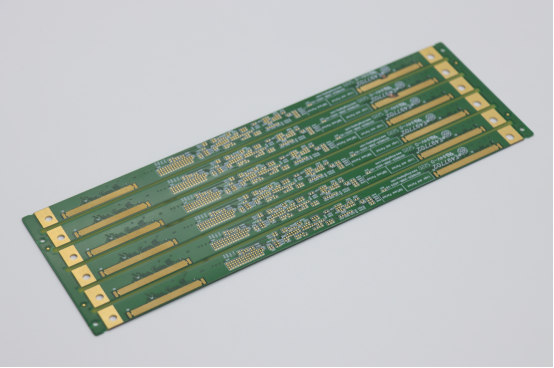
Copper Balancing in PCB Design: A Comprehensive Guide
When designing high-performance PCBs, achieving a perfect balance of copper distribution across layers isn’t just a design choice—it’s a necessity. As PCBs become more intricate, especially with multiple layers, the risks associated with uneven copper coverage can lead to serious issues like warping, delamination, and even mechanical failure. Copper balancing addresses these challenges by ensuring uniform copper distribution, which is crucial for maintaining the integrity and reliability of the final product. In this article, we’ll dive into why copper balancing matters, how it works, and the techniques used to implement it effectively in PCB design. From reducing thermal stress to improving overall durability, copper balancing is essential for anyone designing complex, high-performance electronics.
What Is Copper Balancing and Why Is It Important?
Definition of Copper Balancing
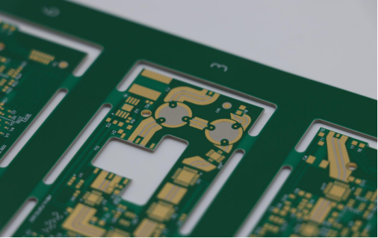
Copper balancing is the process of ensuring an even distribution of copper across all layers of a printed circuit board (PCB). This is essential for maintaining structural integrity and preventing issues like warping or layer separation.
In PCB design, multiple layers of copper are used to create electrical connections. These layers are separated by insulating materials, known as dielectrics. Copper balancing ensures that each layer has a similar amount of copper coverage, usually within a ±10% difference. This equal distribution is crucial for the thermal and mechanical stability of the PCB during the manufacturing process.
For example, if one layer has 30% copper coverage and another has only 10%, the differing amounts of copper will cause those layers to expand and contract at different rates when exposed to heat. This difference in behavior can lead to problems in the finished PCB, such as warping or failure to fit in its enclosure.
Purpose of Copper Balancing
Copper balancing is important because it helps prevent warping, delamination, and mechanical failures in PCBs. It ensures that the board remains stable during manufacturing and use, avoiding costly mistakes or damage.
The main purpose of copper balancing is to reduce "thermal stress," which occurs when layers of a PCB expand and contract at different rates due to temperature changes. For example, when a PCB is heated during the manufacturing process (such as in soldering or lamination), different layers might react differently if the amount of copper in each layer is not balanced. This imbalance can lead to various issues:
Warping: If one layer expands more than another, the board may bend or twist. This warping can make the PCB difficult to handle or cause it to not fit properly in its enclosure.
Delamination: When layers of a PCB are bonded together, the copper and dielectric materials must expand and contract in a coordinated way. If one layer has much more copper than another, the different expansion rates can cause layers to separate, leading to delamination. This is a serious problem because delaminated boards lose their electrical integrity and can short-circuit.
Mechanical Failure: Warped or delaminated PCBs can fail in their intended application. In high-performance electronics, such as medical devices or automotive parts, the board’s performance must remain consistent under stress. Copper balancing helps ensure the mechanical stability of the PCB, preventing failures that could damage the device or render it unreliable.
Example: In the automotive industry, PCBs used in engine control units (ECUs) must withstand extreme temperature changes. If copper balancing is not done properly, the PCB might warp during the reflow soldering process, causing connections to fail or components to become misaligned, leading to costly repairs or replacements. Proper copper balancing prevents such issues, ensuring that the PCB functions reliably in demanding environments.
How Does Copper Balancing Work in PCB Manufacturing?
Copper balancing in PCB manufacturing is a crucial process that ensures even distribution of copper across all layers of the board. This helps manage thermal stress, which could otherwise lead to issues like warping or delamination.
Thermal Stress and Its Impact on PCBs
Thermal stress occurs when different parts of the PCB expand or contract at different rates due to heat. This imbalance can cause warping, delamination, or failure of the PCB. Copper balancing helps to prevent these issues by ensuring uniform copper coverage across all layers.
In PCB manufacturing, temperature changes, like those during the soldering process or lamination, affect the materials differently. Copper and the insulating materials (called dielectrics) expand at different rates when exposed to heat. Copper expands at about 17 parts per million (ppm) per degree Celsius, while dielectrics like FR-4 expand at a lower rate of around 13 ppm per degree Celsius. If one layer has a lot of copper and another has very little, the copper-rich layer will expand more than the other, creating stress between the layers. This uneven stress can result in warping or even separation between the layers (delamination), leading to mechanical failure.
Example: Think of it like stretching two different fabrics in the same direction. One fabric stretches easily while the other barely stretches at all. If you pull them together, the tension between the fabrics can cause them to rip or tear. Similarly, uneven copper distribution causes tension between the layers, which can lead to PCB failure.
Balancing Copper Coverage Across Layers
Copper balancing involves ensuring that the amount of copper on each layer of the PCB is as equal as possible. This is usually done by keeping the copper coverage within a ±10% difference from one layer to another. Equal coverage helps reduce the thermal stress between layers and prevents issues like warping and delamination.
In a typical PCB, especially multilayer boards, different layers of copper are used for signal paths, power distribution, and grounding. If one layer has significantly more copper than another, the board can experience different expansion rates when heated. To avoid this, designers use copper balancing to ensure that the layers have similar amounts of copper coverage. The goal is to keep the copper coverage within a certain range, typically ±10%. For example, if one layer has 30% copper, the adjacent layer should have between 27% and 33% copper coverage. This even distribution ensures that all layers expand and contract at a similar rate, minimizing the risk of warping or delamination.
Example: Imagine you have a 4-layer PCB. If the top layer has 40% copper, and the next layer only has 10%, the difference in copper coverage will cause those layers to expand and contract at different rates. However, if the copper coverage on all layers is kept within a 10% difference, the stress between the layers is minimized, leading to a more stable PCB.
What Are the Key Challenges Copper Balancing Addresses?
Copper balancing addresses several key challenges in PCB manufacturing, primarily related to uneven expansion between copper and dielectric layers. When copper is not evenly distributed across the layers, thermal stress can lead to warping, delamination, and mechanical failures.
Uneven Expansion Between Copper and Dielectric Layers
Copper and dielectric materials expand and contract at different rates when exposed to heat, which can create stress between the layers. Copper balancing ensures that this stress is minimized by distributing copper evenly across all layers of the PCB.
In a PCB, the copper layers are separated by dielectric materials (such as FR-4), which act as insulators. These materials have different thermal expansion rates, meaning they expand and contract at different speeds when exposed to heat. Copper expands more quickly than the dielectric material, which creates a mismatch between the layers during the heating process (like soldering or lamination). This mismatch can lead to stress between the copper and dielectric layers, which can cause warping, separation, or other mechanical problems.
Example: Think of two materials—one that expands more when heated and one that barely changes. If these materials are glued together, the difference in expansion rates could cause them to break apart or bend. Similarly, when copper and dielectric layers expand unevenly, it causes physical issues on the PCB, such as delamination or warping.
Problems Caused by Imbalanced Copper Distribution
Imbalanced copper distribution between layers leads to thermal stress, which can cause warping, delamination, and mechanical failures in the PCB. Copper balancing helps prevent these issues by ensuring even copper coverage.
If copper coverage across the layers of a PCB is uneven, it leads to problems when the board undergoes temperature changes. For instance, if one layer has more copper than another, the copper-rich layer will expand more than the copper-poor layer. This results in physical strain, leading to warping, delamination or mechanical Failures.
Example: In high-performance electronics, such as medical devices or aerospace applications, the stability of the PCB is critical. If the copper coverage is imbalanced, the board may warp or delaminate, which can cause the entire system to fail. For instance, in a pacemaker, a delaminated PCB could lead to electrical malfunctions, which can be life-threatening.
What Techniques Are Used for Copper Balancing in PCB Design?
To ensure even copper distribution across PCB layers, designers use several techniques that help balance thermal stress and maintain the board's structural integrity. These methods include copper pours, mirroring patterns, strategic thieving, and layer stacking optimization.
Copper Pours to Increase Coverage
Copper pours fill large empty spaces in PCB layers with copper, often connected to the ground or power planes, to increase copper coverage and balance thermal stress.
In PCB design, certain areas of the board might have little or no copper, which can lead to uneven thermal expansion and stress between layers. Copper pours are used to fill these empty spaces with solid copper, which is typically connected to the ground or power planes. This technique increases the copper coverage in low-coverage areas, helping to balance the thermal stress and prevent warping or delamination. The added copper ensures that the board's layers expand and contract at similar rates, maintaining the structural integrity of the PCB.
Example: Imagine a 4-layer PCB where the top layer has many components, but the bottom layer has large gaps with no copper. By filling those gaps with copper connected to the ground plane, the overall copper coverage becomes more uniform, reducing the chances of thermal stress issues.
Mirroring Patterns Between Layers
Mirroring patterns involves copying copper shapes from one layer to another to ensure consistent copper coverage across layers.
To balance copper between different layers, designers often use mirroring. This technique involves copying the copper shapes from one layer and transferring them to the corresponding positions on another layer. By duplicating the copper patterns across multiple layers, designers ensure that each layer has a similar amount of copper coverage, reducing the risk of thermal stress. Mirroring is especially effective in maintaining balanced ground and power planes, as these layers often need more copper to handle heat dissipation.
Example: If the ground plane (Layer 2) has a large copper area, the power plane (Layer 3) can mirror these patterns to ensure both layers have similar copper coverage. This reduces the thermal imbalance and minimizes the risk of warping or delamination.
Strategic Thieving for Coverage Adjustment
Thieving involves adding small amounts of non-functional copper in low-coverage areas to balance copper coverage across layers.
Thieving is a technique used to adjust the copper coverage in areas where there is not enough copper. This is done by adding small patches of copper, known as "thieves," to the empty spaces on the board. These added copper sections do not serve any functional purpose; their only role is to increase the copper coverage and balance the thermal expansion between layers. While thieving is not always ideal, it is useful in cases where other methods, like copper pours, are not sufficient or practical.
Example: On a PCB where one layer has only 10% copper coverage, thieving could add small areas of copper throughout the low-coverage section to bring the total coverage closer to the 30% copper level, helping balance thermal stress and prevent board warping.
Layer Stacking Optimization for Multilayer Boards
Layer stacking optimization arranges the layers of the PCB to alternate between high and low copper coverage, ensuring even thermal expansion and reducing stress.
For multilayer PCBs, layer stacking optimization is a critical method for balancing copper across layers. The goal is to arrange the layers so that those with high copper coverage are balanced by layers with lower coverage. This alternating arrangement helps to distribute thermal stress evenly and prevents warping or delamination. By stacking layers in a thoughtful way, designers can ensure that the PCB remains stable during thermal processes like soldering and lamination.
Example: On a 6-layer PCB, a designer might arrange the layers as follows:
Layer 1 (top signal): 30% copper coverage
Layer 2 (ground): 25% copper coverage
Layer 3 (power): 28% copper coverage
Layer 4 (signal): 32% copper coverage
Layer 5 (power): 28% copper coverage
Layer 6 (bottom signal): 30% copper coverage
This balanced stacking of high and low copper coverage layers ensures that all layers expand and contract at similar rates, minimizing thermal stress and mechanical failure.
How Do Designers Implement Copper Balancing in Real-World Projects?
Designers implement copper balancing in real-world PCB projects by using advanced software tools, automating the process, and carefully calculating copper coverage across multiple layers. These techniques ensure even copper distribution, preventing thermal stress and maintaining the PCB’s structural integrity.
Using Advanced PCB Design Software
Designers use advanced PCB design software like Cadence Allegro to analyze and optimize copper coverage across different layers of the PCB. These tools help ensure that copper is evenly distributed, minimizing thermal stress and preventing potential issues like warping or delamination.
Advanced PCB design software allows designers to visualize and calculate copper coverage across multiple layers of a PCB. Tools like Cadence Allegro, Altium Designer, and KiCad are commonly used in the industry to simulate copper distribution. These tools help identify areas where copper is too sparse or too dense, which could cause thermal imbalance. By using these software programs, designers can make real-time adjustments to copper pours, thieving patterns, and layer stacking, ensuring balanced copper distribution throughout the PCB.
Example: Using Cadence Allegro, a designer can generate a visual map of copper coverage across all PCB layers. This allows them to pinpoint areas with insufficient copper and adjust those areas by adding copper pours or adjusting layer stacking to improve balance.
Manual vs. Automated Balancing
Copper balancing can be done manually or with the help of automated software tools. Automated methods, while requiring more initial setup, reduce human error and improve design efficiency.
In the past, copper balancing was largely a manual process, where designers would manually check and adjust the copper coverage on each layer of the PCB. However, with modern software, much of this process can now be automated. Automated tools can quickly analyze the entire PCB and suggest or implement copper balancing adjustments without requiring manual intervention. This significantly reduces the likelihood of errors and helps designers focus on other aspects of the project.
Example: Manually, a designer might have to go through each layer, checking the copper coverage and adding copper pours or thieving by hand. With automated tools, this process is much faster, as the software will calculate and suggest adjustments for copper coverage across all layers in real-time.
Advantages of Software Automation in Reducing Errors
Automated copper balancing helps reduce errors, improves design consistency, and speeds up the design process by automatically calculating and adjusting copper coverage based on preset parameters.
The main advantage of using automated software for copper balancing is the reduction of human error. Manual processes are prone to oversight, leading to inconsistencies or mistakes that could affect the PCB’s performance. Automated systems, on the other hand, are designed to follow specific guidelines and can quickly identify areas of imbalance in the copper distribution. They also help streamline the design process, saving time and reducing the chance of needing costly revisions.
Example: Suppose a designer accidentally overlooks a small area with too little copper coverage, which could cause thermal stress issues. An automated tool would flag this area, alert the designer, and automatically adjust the copper distribution, preventing this issue from affecting the final design.
Calculating Copper Coverage Across Multiple Layers
To ensure copper balancing is effective, designers must calculate copper coverage across all PCB layers. This involves using design software to assess the copper area on each layer and making adjustments where necessary.
Calculating copper coverage involves analyzing the total area of copper on each layer of the PCB. The goal is to ensure that the copper coverage is consistent across layers, typically within a ±10% difference. By using software tools, designers can quickly measure the copper coverage on each layer, identify areas with too much or too little copper, and make necessary adjustments. This process ensures that all layers of the PCB will expand and contract at the same rate when exposed to heat, preventing warping and other thermal stress issues.
Step-by-Step Design Considerations:
1. Initial Analysis: Use the software to assess copper coverage across all layers of the PCB.
2. Identify Imbalances: Look for areas with sparse or dense copper coverage that may cause thermal stress.
3. Make Adjustments: Add copper pours or use thieving to increase coverage in low areas.
4. Verify Balance: Ensure that the copper distribution on each layer is within a 10% range to prevent issues like warping or delamination.
5. Finalize the Design: Once copper balancing is optimized, finalize the PCB layout for production.
Example: If a designer finds that one layer has 50% copper coverage and another has only 15%, they can use the software to adjust the layers to a more balanced coverage, such as bringing the low-coverage layer closer to 30%. This ensures uniform expansion during manufacturing and prevents potential issues.

What Are the Pros and Cons of Copper Balancing?
Copper balancing offers significant advantages, such as preventing warping, reducing delamination, and improving thermal management. However, it also comes with challenges, including increased design time and potential increases in thickness and weight.
Benefits of Copper Balancing
Copper balancing offers several advantages. These benefits ensure the reliability and longevity of the board in various applications.
Prevents Warping: One of the primary benefits of copper balancing is its ability to prevent warping in PCBs. When copper is evenly distributed across all layers, each layer expands and contracts at the same rate when exposed to heat. This uniform expansion prevents the board from bending or twisting during manufacturing processes, such as soldering or lamination.
Reduces Delamination: Copper balancing also reduces the risk of delamination, which occurs when layers of the PCB separate due to thermal stress. By ensuring that copper coverage is even across all layers, the board is less likely to experience stress between the layers, keeping them securely bonded.
Enhances Mechanical Durability: Even distribution of copper improves the mechanical durability of the PCB. Balanced copper layers reduce the stress that can cause solder joints or components to crack, increasing the lifespan of the PCB in challenging environments.
Improves Thermal Management: Copper is an excellent conductor of heat. When it is evenly distributed across the layers of the PCB, it helps dissipate heat more effectively. This improves the overall thermal management of the board, preventing overheating and ensuring stable performance.
Challenges and Drawbacks of Copper Balancing
While copper balancing offers significant benefits, it also presents challenge. These factors need to be considered during the design process.
Increased Design Time: One of the main drawbacks of copper balancing is the additional time required to design the PCB. Ensuring that copper is evenly distributed across all layers involves detailed calculations and adjustments, which can slow down the design process. Designers must manually or automatically check and adjust the copper coverage on each layer, which can be time-consuming.
Potential Thickness and Weight Increases: Copper balancing sometimes requires adding more copper to certain areas of the PCB, which can increase the overall thickness and weight of the board. In applications where space and weight are critical, such as wearable devices or drones, this can be a significant downside.
Where Should Copper Balancing Be Applied in PCB Design?
Copper balancing should be applied in specific PCB designs where thermal stress, reliability, and mechanical durability are critical. This includes multilayer PCBs, high-temperature environments, and structurally critical applications such as medical devices, aerospace, and military electronics.
Multilayer PCBs (4 Layers and Beyond)
Copper balancing is crucial in multilayer PCBs, especially those with 4 or more layers, to ensure uniform thermal expansion and prevent issues like warping or delamination.
In more complex PCB designs with multiple layers, copper balancing becomes increasingly important. A multilayer PCB, such as a 4-layer or 6-layer board, has different copper planes for signal routing, power distribution, and grounding. If these layers have uneven copper coverage, thermal expansion during manufacturing can cause the layers to expand and contract at different rates. This uneven behavior leads to stress between the layers, potentially causing warping, delamination, or mechanical failure.
For example, in a 6-layer PCB, layers with more copper will expand more than those with less. To avoid these issues, designers ensure that copper coverage is balanced between layers, maintaining structural integrity and preventing physical defects in the final product.
Example: In consumer electronics like smartphones, a 6-layer PCB is commonly used to pack more components into a compact space. Copper balancing ensures that the board remains flat and intact during manufacturing and use, reducing the risk of failure due to thermal stress.
High-Temperature Environments
Copper balancing is essential for PCBs used in high-temperature environments, to ensure effective thermal management and prevent heat-related issues.
PCBs used in high-temperature environments, such as those found in automotive engines, industrial machines, or aerospace systems, must be able to withstand extreme temperature fluctuations. These environments cause different materials within the PCB to expand and contract at varying rates. Without copper balancing, these temperature changes can cause warping, delamination, or even failure of electrical connections.
Balancing the copper ensures that the board maintains its shape and functionality even when exposed to heat, as the copper and dielectric materials expand at similar rates. This helps to prevent overheating, thermal fatigue, and loss of signal integrity, ensuring that the PCB remains reliable over time.
Example: In automotive electronics, such as engine control units (ECUs), the PCB must survive temperatures that range from –40°C to 125°C. Copper balancing in these PCBs prevents warping and delamination, ensuring the board can endure extreme temperatures without losing performance.
Structurally Critical Applications
Copper balancing is especially important in structurally critical applications, where reliability and durability are paramount.
In applications like medical devices, and aerospace electronics, the reliability of the PCB is critical. These devices are often subjected to extreme environmental conditions, including high temperatures, vibrations, and mechanical stresses. Even minor PCB failure can lead to catastrophic results, such as equipment malfunction or compromised safety.
Copper balancing ensures that the PCB can endure these harsh conditions. By distributing copper evenly across layers, designers minimize thermal stress, mechanical strain, and the risk of delamination, ensuring that the PCB remains intact and fully functional under extreme conditions.
Example: In pacemakers, where failure can result in life-threatening situations, copper balancing ensures that the PCB remains durable, even with the constant temperature variations and mechanical stresses the device experiences. By balancing copper across the layers, the integrity of the PCB is maintained, ensuring continuous and reliable operation.
What Are the Best Practices for Copper Balancing in PCB Manufacturing?
To ensure effective copper balancing in PCB manufacturing, it’s important to follow best practices throughout the design and testing process. These practices include conducting an initial thermal analysis, continuously monitoring copper distribution during the design phase, and validating the PCB’s thermal and mechanical performance post-design.
Pre-Design Considerations
Before starting the PCB design, it’s essential to conduct an initial thermal analysis and choose appropriate materials to ensure copper balancing can be effectively implemented.
Initial Thermal Analysis and Material Selection:
Before designing a PCB, it’s important to consider how the PCB will perform under heat. A thermal analysis identifies potential hot spots where copper coverage needs to be more uniform to prevent thermal issues. This step helps designers understand how heat will flow through the board and what parts of the PCB will be exposed to the most thermal stress. Using this information, designers can choose materials with matching thermal expansion rates, like selecting appropriate dielectric materials that expand at similar rates to copper. This pre-design analysis helps prevent issues later, making sure the board will perform well in high-temperature environments.
Example: In automotive applications, where the PCB is exposed to extreme temperature changes, performing a thermal analysis helps ensure that areas exposed to high heat, like near the engine, are designed with more copper coverage to prevent warping or delamination.
During-Design Practices
During the design phase, continuous monitoring of copper distribution is essential to ensure that copper is balanced correctly across the PCB layers.
Regular Monitoring of Copper Distribution:
During the design process, it’s critical to regularly check the copper coverage on all layers of the PCB. This can be done using advanced PCB design software like Cadence Allegro or Altium Designer, which allows designers to see the distribution of copper across each layer in real-time. By monitoring copper distribution, designers can identify areas with too much or too little copper and make adjustments before finalizing the design. Consistent checking ensures that the PCB remains thermally balanced and can handle heat expansion without any issues.
Example: In a 4-layer PCB for a consumer electronics device, the designer might notice that the bottom layer is copper-poor. Using the software, they can adjust the design by adding copper pours or mirroring copper patterns from other layers, ensuring that all layers have similar copper coverage.
Post-Design Testing
After the design is complete, post-design testing is crucial to validate the thermal and mechanical performance of the PCB, ensuring that the copper balancing is effective.
Validating Thermal and Mechanical Performance:
Once the PCB design is finalized, it’s important to conduct post-design testing to validate that the copper balancing has achieved its intended results. This testing typically involves subjecting the PCB to the same environmental conditions it will face in real-life applications, such as thermal cycling (extreme temperature changes) and mechanical stress (vibration or pressure). By observing how the PCB performs under these conditions, designers can confirm that the copper is evenly distributed and that the board won’t warp, delaminate, or fail during normal use.
Example: In aerospace applications, where the PCB must withstand rapid temperature changes from the high altitudes to the ground, post-design testing might involve thermal cycling tests to simulate these conditions. The PCB is heated and cooled repeatedly to see if the copper distribution causes any stress or failures, ensuring the board's reliability in real-world use.
How Does Copper Balancing Affect PCB Reliability?
Copper balancing plays a crucial role in enhancing PCB reliability by ensuring even copper distribution across all layers. This practice helps improve the long-term performance of the PCB, especially in harsh environments, while also enhancing signal integrity and reducing electromagnetic interference (EMI).
Impact on Long-Term PCB Performance
Copper balancing plays a significant role in improving the long-term performance of a PCB by preventing physical defects and ensuring the board can withstand environmental stresses over time.
Copper balancing contributes to the long-term reliability of PCBs by ensuring that the layers expand and contract at similar rates during thermal cycles. Uneven copper distribution can cause warping or delamination over time, which can lead to mechanical failure or loss of functionality. Balanced copper distribution helps the PCB resist damage from repeated thermal changes, such as heating and cooling during operation. This ensures that the board performs well over its expected lifespan, even in challenging environments.
Example: In automotive PCBs, where temperature fluctuations are common, copper balancing helps ensure that the board maintains its integrity over the years. A balanced copper distribution ensures that the board can endure high heat from engine components or sudden cooling without warping or delaminating, which could otherwise lead to failure.
Reliability Improvements in Harsh Environments
Copper balancing is essential for PCBs used in harsh environments, such as automotive, industrial, or aerospace applications, where temperature extremes, vibration, and mechanical stress are frequent.
PCBs that operate in harsh environments, such as those in cars, factories, or airplanes, are subjected to a wide range of physical and thermal stresses. Copper balancing helps to maintain the mechanical integrity of the PCB under these conditions by ensuring even thermal expansion and reducing stress between layers. In high-stress situations, this prevents the PCB from warping, cracking, or delaminating, which could otherwise lead to circuit failure or performance degradation.
Example: In aerospace, where PCBs are exposed to extreme temperature differences between high altitudes and the ground, copper balancing ensures that the board remains flat and intact. This reliability is crucial for safety-critical applications, such as avionics, where any failure could be catastrophic.
Effect on Signal Integrity and Electromagnetic Interference (EMI)
Copper balancing improves signal integrity and reduces electromagnetic interference (EMI) by maintaining consistent copper coverage, which helps to stabilize the electrical performance of the PCB.
Signal integrity refers to the quality of the electrical signals transmitted through the PCB. Uneven copper distribution can lead to signal loss or distortion, affecting the performance of sensitive electronic components. By balancing the copper layers, designers ensure that the PCB maintains a uniform electrical environment, reducing noise and interference. Balanced copper coverage also contributes to better grounding and shielding, which reduces electromagnetic interference (EMI) and enhances the overall electrical performance.
Example: In high-frequency applications like mobile phones or computers, copper balancing helps ensure that the signal transmission remains clear and reliable. This reduces the likelihood of signal degradation or interference, allowing devices to operate efficiently without disturbances that can impact the user experience or system performance.
Conclusion
Copper balancing is a vital technique for ensuring the reliability, durability, and optimal performance of PCBs, especially in challenging environments. By maintaining uniform copper distribution, it helps prevent common issues like warping, delamination, and signal interference. Whether in automotive, aerospace, or consumer electronics, copper balancing ensures that PCBs remain functional and dependable over time.
For those seeking high-quality, reliable PCB solutions, PCBMASTER, a seasoned PCB supplier, offers expert design and manufacturing services to meet your specific needs. With years of experience in producing advanced PCBs, they provide customized solutions that ensure optimal performance for your projects. Trust PCBMASTER to deliver the best in copper balancing and PCB manufacturing expertise.
FAQ Section: Common Questions About Copper Balancing
1. Why is copper balancing necessary in multilayer PCBs?
Copper balancing is essential in multilayer PCBs because different layers expand at different rates during temperature changes. If copper distribution is uneven, it can lead to warping, delamination, or mechanical failure. Even copper coverage ensures that the board remains structurally sound, preventing stress between layers during manufacturing or operation.
Example: In automotive PCBs, where temperature changes are frequent, copper balancing prevents warping and ensures long-term reliability.
2. Can copper balancing help reduce PCB manufacturing costs?
While copper balancing requires additional design time, it can reduce long-term costs by preventing failures, rework, or product recalls. Proper copper distribution ensures the board’s durability, reducing the need for costly repairs or replacements due to warping or delamination.
Example: A PCB that fails due to improper copper distribution in an automotive application could lead to expensive recalls. Copper balancing helps avoid such issues.
3. What are the common signs of poor copper balancing in PCBs?
Common signs of poor copper balancing include:
Warping: Uneven copper causes the PCB to bend during manufacturing.
Delamination: Layers separate due to thermal stress.
Mechanical Failure: Cracks or broken connections caused by uneven expansion.
Electrical Failures: Signal degradation due to inconsistent copper coverage.
Example: If a mobile device’s PCB shows visible warping or layer separation, it’s likely due to improper copper balancing.
4. How does copper balancing improve thermal management in PCBs?
Copper balancing helps spread heat evenly across the PCB, preventing hot spots and improving heat dissipation. This ensures that components stay cool and prevents thermal expansion issues, keeping the board’s structure intact.
Example: In high-performance PCs, copper balancing helps dissipate heat efficiently, preventing overheating of critical components like processors.
5. What are the most common tools used for copper balancing in PCB design?
Common tools for copper balancing include:
Cadence Allegro: Advanced copper coverage analysis.
Altium Designer: Real-time copper distribution monitoring.
KiCad: Open-source tool for copper balancing.
Autodesk Eagle: Helps automate copper distribution adjustments.
Mentor Graphics PADS: Used for precise copper balancing in high-performance designs.
Example: A designer might use Cadence Allegro to simulate the copper distribution in a high-power PCB, ensuring proper thermal management.
Author Bio
Hi, I'm Carol, the Overseas Marketing Manager at PCBMASTER, where I focus on expanding international markets and researching PCB and PCBA solutions. Since 2020, I've been deeply involved in helping our company collaborate with global clients, addressing their technical and production needs in the PCB and PCBA sectors. Over these years, I've gained extensive experience and developed a deeper understanding of industry trends, challenges, and technological innovations.
Outside of work, I'm passionate about writing and enjoy sharing industry insights, market developments, and practical tips through my blog. I hope my posts can help you better understand the PCB and PCBA industries and maybe even offer some valuable takeaways. Of course, if you have any thoughts or questions, feel free to leave a comment below—I'd love to hear from you and discuss further!

