


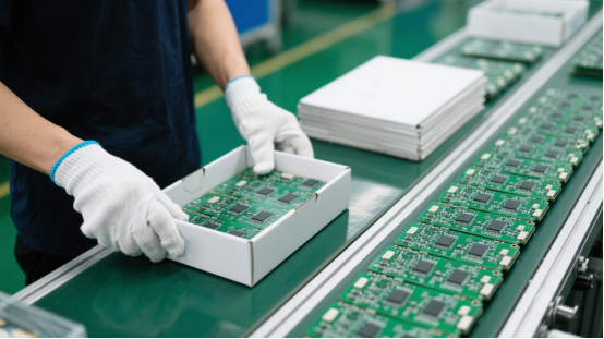
PCB Assembly Main Process: From Components to Boards
Printed Circuit Board (PCB)assembly is the stage where electronic design becomes reality. During this process, components are mounted, soldered, and connected on a printed circuit board to create a fully functional device.
From the first layer of solder paste to the final quality test, each step determines the reliability and performance of the end product. PCB assembly plays a vital role across industries—from industrial control systems to IoT and consumer electronics—where precision and consistency are essential.
Understanding the PCB Assembly Process
What Is PCB Assembly?
PCB assembly is the process of mounting electronic components onto a printed circuit board to create a fully functional electronic device. It differs from PCB fabrication, which involves producing the bare board itself—etching copper traces, drilling holes, and applying solder masks. In short, fabrication creates the “canvas,” while assembly brings it to life with components and electrical connections.
The main goals of PCB assembly are:
Component placement: Ensuring each resistor, capacitor, IC, and connector is correctly positioned.
Electrical connectivity: Establishing reliable connections between components through soldering.
Device reliability: Guaranteeing the assembled board can operate as intended under expected conditions.
PCB assembly can be performed manually or automatically. Manual assembly is typically used for prototypes, small batches, or large components that require precise human handling. Automated assembly, often using pick-and-place machines and reflow ovens, is used in mass production for speed, accuracy, and consistency.
Key Types of PCB Assembly
PCB assembly generally falls into three main types:
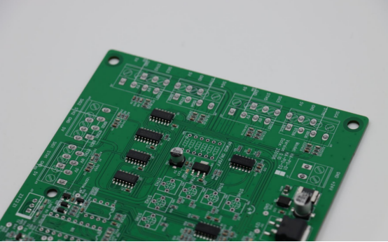
1. Through-Hole Assembly (THA)
Components with wire leads are inserted into drilled holes on the PCB and soldered on the opposite side. This method offers strong mechanical connections, making it ideal for connectors, large capacitors, and components that are subjected to mechanical stress.
2. Surface Mount Technology (SMT)
Components are mounted directly onto the surface of the PCB using solder paste. This method enables the use of smaller components, allows for higher component density, and supports faster automated assembly. Most modern electronics rely on surface-mount technology (SMT) for its efficiency and ability to achieve miniaturization.
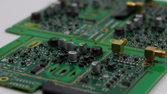
3. Mixed Technology Assembly
This approach combines surface-mount technology (SMT) and through-hole assembly (THA) on the same board. It is particularly useful for complex designs that require both high-density surface-mounted components and durable through-hole parts, such as power connectors or specialized sensors.
Example Comparison: SMT vs. Through-Hole
| Feature | SMT | Through-Hole |
|---|---|---|
| Assembly Speed | Fast (automated) | Larger components only |
| Component Size | Small, compact | Larger components only |
| Cost Efficiency | Lower cost in large production | Higher cost due to manual labor |
Mechanical Strength | Moderate | High, suitable for stress points |
In summary, the choice of assembly type depends on design complexity, production volume, and component requirements. Modern boards often use SMT for most components, with THA reserved for specialized parts.
Step-by-Step PCB Assembly Main Process
Step 1 – Solder Paste Application
Solder paste application is the foundation of successful surface-mount PCB assembly. It involves depositing a mixture of flux and fine solder particles onto PCB pads using a stencil that aligns precisely with the pads.
Importance of correct thickness:
Thin paste may lead to weak joints or components not adhering.
Excess paste can create solder bridging, short circuits, or tombstoning of small components.
Typical paste thickness ranges from 100–150 microns for standard SMD pads.
Alignment: The stencil must be perfectly aligned with the PCB pads. Misalignment can cause solder on wrong pads or incomplete connections.
Common issues: Misregistration, air bubbles in paste, and uneven deposition.
Example:
Manual printing: Operator uses a squeegee to apply paste. Accuracy depends on skill; suitable for small prototypes.
Automated stencil printer: Uses precision alignment cameras and controlled squeegee pressure to ensure uniform paste deposition, improving yield for mass production.
Step 2 – Pick and Place of Components
After solder paste deposition, components are placed on the board. Pick-and-place machines handle this process with high speed and precision.
Function: Vacuum nozzles pick components from feeders or trays and place them on pads covered with solder paste.
Handling small SMD parts: Components can be as small as 01005 (0.4 mm × 0.2 mm), requiring precise vision systems and fine nozzle control.
High-density boards: Machines adjust placement order and pressure to avoid displacing neighboring components.
Tolerance: Placement accuracy often within ±0.05 mm for standard SMDs; critical for high-speed digital circuits.
Example: For a board with 2,000 SMD components, automated machines can complete placement in minutes, while manual placement could take hours with higher error rates.
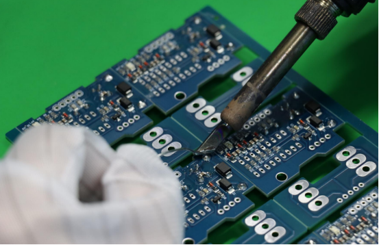
Step 3 – Reflow Soldering Process
Reflow soldering melts the solder paste to form solid, reliable joints between components and PCB pads.
Temperature profile stages:
Preheat: Gradually raises the board temperature to avoid thermal shock (typically 150–180°C).
Soak: Maintains uniform temperature to activate flux and reduce thermal gradients.
Reflow: Peaks typically 230–250°C to melt solder fully.
Cooling: Rapid, controlled cooling solidifies joints without stressing components.
Factors affecting solder quality: Oven temperature uniformity, conveyor speed, flux type, solder alloy composition.
Examples:
Convection reflow: Hot air circulates around the board; widely used for standard SMT boards.
Vapor phase reflow: Uses vaporized fluid for uniform heat transfer; reduces risk for temperature-sensitive components.
Step 4 – Inspection and Quality Control
Inspection ensures defects are detected before final testing, preventing functional failures.
Visual inspection: Operator checks for obvious defects, such as missing or misaligned components.
Automated Optical Inspection (AOI): Cameras compare each board against the design; detects solder bridging, missing components, or polarity errors.
X-ray inspection: Essential for hidden solder joints like Ball Grid Array (BGA) packages.
Common defects:
Tombstoning: Component rises on one end due to uneven solder paste.
Bridging: Unintended solder connection between pads.
Cold joints: Poorly melted solder, causing weak electrical connection.
Rework and repair: Soldering irons or hot-air stations correct defective joints; AOI can verify repairs.
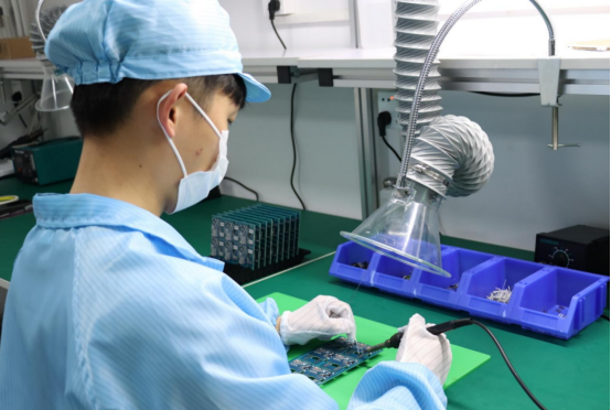
Step 5 – Through-Hole Component Insertion (if applicable)
Some components require insertion into drilled holes instead of surface mounting.
Process: Components with leads are placed into holes, then soldered manually or via wave soldering.
When to choose mixed-technology assembly:
Heavy connectors, switches, or large capacitors that experience mechanical stress.
Boards combining compact SMT ICs and durable through-hole parts.
Example: On a power supply board, large electrolytic capacitors are through-hole for mechanical stability, while control ICs are SMT for compactness.
Step 6 – Final Testing and Function Verification
Final testing ensures the assembled PCB works correctly under intended conditions.
Electrical tests:
In-Circuit Testing (ICT): Checks each component and its connection for continuity, resistance, and correct placement.
Functional Circuit Testing (FCT): Simulates device operation to verify that the PCB performs its intended function.
Reliability assurance:
Burn-in testing: Operates boards under elevated voltage and temperature to detect early failures.
Environmental stress screening: Tests for performance under vibration, humidity, and thermal cycling.
Goal: Detect latent defects and ensure boards meet performance and durability standards before shipping.
Materials and Equipment in PCB Assembly
Essential Tools and Machines
PCB assembly relies on specialized tools and machines to ensure accuracy, speed, and quality. The key equipment includes:
Stencil Printer: Deposits solder paste precisely on the PCB pads, using a metal stencil that matches the pad layout. Accuracy is critical for high-density boards.
Pick-and-Place Machine: Automatically picks components from reels or trays and places them on the solder-pasted PCB with high precision. Handles even tiny 01005 components on compact boards.
Reflow Oven: Melts the solder paste to form strong joints. Controlled temperature profiles ensure reliable connections without damaging components.
Wave Solder Machine: Primarily used for through-hole components; molten solder wave solders multiple leads simultaneously for speed and consistency.
Automated Optical Inspection (AOI) Systems: Cameras detect defects like misaligned components, solder bridges, or missing parts. Critical for quality control in mass production.
Example – SMT Lines for Prototype vs. Mass Production:
Prototype SMT Line: Smaller, flexible machines allow manual adjustments and quick changeovers for testing different designs. Slower throughput but high adaptability.
Mass Production SMT Line: High-speed automated machines, including multi-head pick-and-place and large reflow ovens, optimize throughput while maintaining precise component placement.
Materials Used
The right materials are essential to ensure strong electrical connections and long-term reliability of assembled PCBs.
Solder Paste: A mixture of flux and solder powder, deposited on pads before component placement. Ensures mechanical and electrical bonds between component leads and PCB pads.
Flux: Promotes wetting of the solder and prevents oxidation during reflow or wave soldering.
PCB Boards: Substrate boards with copper traces, solder mask, and surface finish. Quality affects assembly success and long-term reliability.
Electronic Components: Resistors, capacitors, ICs, connectors, and other parts that must meet specifications and tolerances for proper function.
Lead-Free vs. Leaded Solder:
Lead-Free Solder: Complies with RoHS regulations; environmentally friendly but requires higher reflow temperatures.
Leaded Solder (SnPb): Lower melting point, easier to work with, but restricted in many regions due to environmental regulations.
Importance of Storage and Handling:
Moisture Sensitivity: Many SMD components absorb moisture; improper storage can lead to solder defects like popcorn cracking during reflow.
ESD Protection: Electrostatic discharge can damage sensitive ICs; proper grounding, ESD-safe trays, and mats are essential.
Temperature Control: Solder paste and flux have shelf lives and require refrigeration in some cases to maintain performance.
Common Challenges in PCB Assembly
Soldering Defects
Soldering defects are among the most frequent issues in PCB assembly and can directly affect board reliability. Common types include:
Bridging: Occurs when excess solder connects two or more adjacent pads, causing a short circuit.
Causes: Too much solder paste, misalignment during placement, or improper reflow temperature.
Prevention: Use accurate stencil thickness, ensure proper component alignment, and monitor reflow oven profiles.
Insufficient Solder: Leads to weak mechanical and electrical connections.
Causes: Inadequate paste deposition, uneven stencil printing, or solder paste drying.
Prevention: Maintain consistent stencil application, check paste viscosity, and control storage conditions.
Voids: Small air pockets in solder joints that reduce thermal and electrical conductivity.
Causes: Trapped flux gases during reflow.
Prevention: Optimize reflow profile, ensure proper solder paste formulation, and avoid excessive board contamination.
Component Placement Issues
Incorrect component placement can compromise electrical functionality or board reliability. Common issues include:
Misalignment: Component shifted from intended pad location.
Tombstoning: One end of a component lifts off the pad during reflow due to uneven solder surface tension.
Missing Components: Components not placed due to feeder issues or machine errors.
Prevention and Solutions:
Machine Calibration: Regular calibration of pick-and-place machines ensures accurate positioning.
Vision Systems: Camera-based alignment verifies component orientation and detects missing or incorrectly placed parts before reflow.
Example: On a high-density board, precise vision-assisted placement prevents 0201 resistors from being misaligned, reducing rework time.
Environmental and Handling Factors
PCB assembly is highly sensitive to environmental conditions and material handling practices.
Moisture Sensitivity: SMD components can absorb moisture from the air. During reflow, trapped moisture can vaporize, causing popcorning, where components crack or lift.
ESD (Electrostatic Discharge) Protection: Sensitive ICs can be damaged by static electricity. Use grounded mats, wrist straps, and ESD-safe storage trays.
Temperature Control: Extreme heat or humidity can affect solder paste viscosity, flux activity, and component performance.
Example: High humidity can increase solder paste viscosity, making deposition uneven. This can lead to insufficient solder joints and defects like bridging or tombstoning. Proper storage and controlled assembly environments maintain consistent soldering quality.
Quality Standards and Certifications
Key Industry Standards
Quality standards provide benchmarks to ensure PCB assemblies are consistent, reliable, and safe. The most important standards include:
IPC-A-610: Defines acceptability criteria for electronic assemblies, including solder quality, component placement, and board cleanliness. Widely used by manufacturers to ensure assembly quality meets industry expectations.
ISO 9001: Focuses on quality management systems. Ensures that production processes are well-documented, repeatable, and continuously improved.
RoHS Compliance (Restriction of Hazardous Substances): Regulates the use of lead, mercury, cadmium, and other hazardous materials in electronic assemblies. Ensures environmentally safe production.
Benefits of Following Standards:
Consistency: Each board meets predefined quality criteria.
Reliability: Reduces defects, enhancing long-term performance of electronic devices.
Global Acceptance: Customers and regulatory authorities recognize compliance as a mark of quality.
Example: A manufacturer adhering to IPC-A-610 ensures that solder joints, whether SMT or through-hole, meet strict visual and functional criteria, minimizing returns and warranty claims.
Inspection and Documentation
Inspection and proper record-keeping are critical for traceability, accountability, and customer confidence.
Traceability Systems: Track each board from component sourcing to final assembly. Each batch is linked to suppliers, machine settings, and operator data.
Production Record-Keeping: Maintains detailed logs of assembly steps, inspections, test results, and rework activities. This allows easy investigation if a defect arises later.
Batch Testing and Certification: Performing sample tests on each production batch ensures that products meet electrical and mechanical specifications. Certification demonstrates compliance to clients and regulatory bodies.
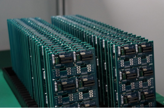
Example: For a production run of 5,000 boards, recording all component lots, solder paste batch numbers, and reflow oven profiles allows any defective board to be traced back to its source, enabling rapid corrective action.
Importance: Consistent documentation and testing not only maintain product quality but also build customer trust, reduce liability, and support continuous improvement initiatives.
Optimizing the PCB Assembly Process
Design for Assembly (DFA) Best Practices
Design for Assembly (DFA) focuses on creating PCB layouts that simplify assembly, reduce errors, and improve manufacturing efficiency.
Layout Tips:
Maintain proper spacing between components to prevent solder bridging. Standard minimum spacing varies with component size; e.g., 0.5 mm between 0603 resistors.
Align polarized components (diodes, LEDs, capacitors) consistently to reduce assembly errors.
Group similar components together to optimize pick-and-place sequences and minimize nozzle changes.
Example: On a high-density board, placing resistors in uniform rows with identical orientation allows pick-and-place machines to operate faster and reduces the chance of misalignment.
Benefit: A well-designed layout simplifies soldering, reduces rework, and improves overall production yield.
Cost and Efficiency Optimization
Optimizing PCB assembly involves balancing production cost, speed, and yield to maximize efficiency.
Batch Size Optimization: Producing in optimal batch sizes reduces setup time and minimizes inventory costs. Smaller batches are flexible for prototypes; larger batches are cost-effective for mass production.
Equipment Maintenance: Regular calibration and preventive maintenance of pick-and-place machines, reflow ovens, and AOI systems prevent downtime and reduce defect rates.
Yield Improvement: Continuous monitoring of defects, rework logs, and production data allows targeted improvements in assembly processes.
Automation and Data Tracking: Automated lines with sensors and integrated software track every board, component lot, and machine setting.
Example: Real-time monitoring of placement accuracy and solder temperature profiles enables immediate corrections, reducing scrap rates and increasing throughput.
Future Trends in PCB Assembly
The PCB assembly industry is evolving with advanced technologies aimed at improving precision, efficiency, and reliability.
AI-Driven Quality Control: Artificial intelligence algorithms analyze AOI and X-ray inspection data to detect defects faster and with higher accuracy than human inspection.
Smart Manufacturing: IoT-enabled machines communicate in real-time, adjusting process parameters automatically to maintain consistent quality.
Miniaturization and Advanced Packaging: High-density components like Ball Grid Array (BGA) and Chip-Scale Package (CSP) enable smaller boards with more functionality, requiring precise placement, advanced soldering techniques, and careful thermal management.
Example: Smart SMT lines now adjust reflow oven temperature zones dynamically based on board size, component mix, and solder type, ensuring defect-free assembly even for complex miniaturized designs.
Conclusion
PCB assembly transforms a bare board into a fully functional electronic device through a series of precise steps: solder paste application, component placement, reflow soldering, inspection, through-hole insertion when needed, and final testing. Each stage requires attention to detail, proper equipment, and strict quality control to ensure reliable performance.
Precision and inspection are critical throughout the process. Accurate component placement, correct soldering, and thorough quality checks prevent defects and improve product yield. Continuous monitoring and process optimization, including design for assembly and automation, further enhance efficiency and reliability.
For businesses and engineers looking to produce high-quality boards, working with experienced PCB assembly partners or service providers, such as PCBMASTER, ensures that every step, from materials handling to final testing, meets industry standards and performance expectations. Partnering with the right team helps reduce risks, save time, and achieve consistent, high-quality results.
FAQs
1. What is the difference between PCB fabrication and PCB assembly?
PCB fabrication is the process of creating a bare printed circuit board (PCB) from raw materials. It involves:
Layer preparation: Laminating copper layers and insulating substrates.
Etching: Removing unwanted copper to form circuit traces.
Drilling: Creating holes for through-hole components or vias.
Surface finishing: Applying solder masks, silkscreens, and surface finishes like HASL or ENIG.
PCB assembly, on the other hand, takes the fabricated board and populates it with components to create a functional electronic device. It involves:
Solder paste application on pads.
Component placement using pick-and-place machines or manual methods.
Soldering (reflow for SMT, wave soldering for through-hole).
Inspection and testing to verify electrical and mechanical functionality.
Key difference: Fabrication produces the physical board structure, while assembly brings the design to life by adding components and making electrical connections.
2. How does reflow soldering work in the PCB assembly process?
Reflow soldering is a method used to solder surface-mount components onto a PCB. The process works as follows:
Preheat stage: The board is gradually heated to 150–180°C to avoid thermal shock.
Soak stage: Temperature is held to activate flux, remove oxides, and ensure uniform heating.
Reflow stage: Temperature peaks (typically 230–250°C) to melt the solder paste, creating mechanical and electrical bonds between components and pads.
Cooling stage: The board is cooled in a controlled manner to solidify solder joints without stressing components.
Factors affecting quality:
Solder paste type and composition.
Reflow oven temperature uniformity and conveyor speed.
Component size, density, and placement accuracy.
Example: Convection reflow ovens use hot air to melt solder, while vapor-phase reflow offers precise temperature control for sensitive components, reducing risk of overheating or thermal stress.
3. What are the most common defects found in PCB assembly?
Common PCB assembly defects include:
Solder bridging: Excess solder creates an unintended connection between pads, causing short circuits.
Insufficient solder: Too little solder leads to weak mechanical and electrical connections.
Cold joints: Poorly melted solder creates unreliable connections.
Tombstoning: One end of a small component lifts off the pad due to uneven solder surface tension.
Misaligned or missing components: Caused by machine placement errors or human mistakes.
Voids: Air pockets in solder joints reduce conductivity and heat transfer.
Prevention methods: Proper stencil design, machine calibration, flux selection, controlled reflow profiles, and thorough inspection.
4. Why is inspection so critical after soldering?
Inspection after soldering ensures that all electrical and mechanical connections are correct and reliable:
Detect defects early: Identify solder bridges, misaligned components, cold joints, or missing parts before final testing.
Reduce rework and scrap: Fix issues before products move to functional testing or shipping.
Ensure reliability: Prevent latent failures in the field, improving device performance and reducing warranty claims.
Methods: Inspection methods include visual checks for obvious defects, automated optical inspection (AOI) for high-density or small components, and X-ray inspection for hidden joints, such as those found in BGA packages.
Example: AOI can detect misaligned 0201 resistors on high-density boards, preventing functional failures after assembly.
5. How can I optimize my PCB design for easier assembly?
Design for Assembly (DFA) improves manufacturability, reduces errors, and increases yield. Key practices include:
Component spacing: Maintain sufficient distance between pads to avoid solder bridging. For example, 0.5 mm spacing for 0603 resistors.
Consistent orientation: Align polarized components in the same direction to reduce placement errors.
Grouping similar components: Place identical components together to speed up pick-and-place operations.
Minimize manual operations: Design boards with mostly SMT components to take advantage of automation.
Accessible test points: Include clear test pads for functional and in-circuit testing.
Example: On a dense IoT board, placing all 0402 resistors in uniform rows with the same orientation allows faster, error-free placement by pick-and-place machines.
Outcome: DFA reduces assembly time, lowers defect rates, and improves reliability, while supporting high-volume automated production.

