


PCB Half Cut: Essential Guide for Designing and Implementing castellated holes
Introduction
Curious about PCB half cuts and their role in modern electronics? PCB half cuts—also known as castellated holes—create strong solder joints between circuit boards, which are crucial for compact and modular designs. This article will explain their purpose, design tips, and manufacturing processes related to PCB half cuts. Understanding PCB half cuts is essential for anyone looking to optimize their electronic designs.
Key Takeaways
·PCB half cuts, or castellated holes, enhance modular designs by enabling effective board-to-board soldering and improving reliability in electronic modules.
·Key design considerations for PCB half cuts include maintaining proper hole diameter, alignment, and pad design to ensure reliable solder connections and performance.
·The manufacturing process for PCB half cuts involves specialized techniques such as drilling, copper plating, and quality control measures to ensure precision and functionality.
Understanding PCB Half Cut and Castellated Holes
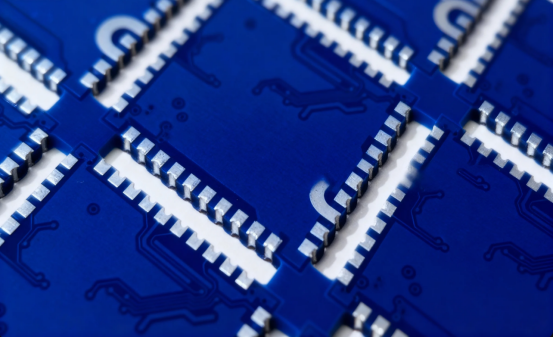
PCB half cuts, also known as castellated holes, involve creating partial cuts on the board to facilitate board-to-board soldering connections. These features are crucial in PCB design as they enhance the reliability of solder joints and allow for compact, modular designs. From Bluetooth to Wi-Fi modules, castellated holes play a pivotal role in modern electronics, enabling seamless integration and functionality.
The manufacturing process of PCBs with half cuts is a sophisticated one, integrating multiple specialized techniques to ensure precise cutting and functionality. Copper plating, for instance, is applied to provide a conductive pathway through the castellated holes, establishing essential electrical connections between board layers. Understanding these intricate details sets the foundation for designing and implementing effective PCB half cuts.
Definition and Purpose of PCB Half Cut
The primary purpose of PCB half cuts is to:
·Create effective solder connections between boards, particularly in modular designs.
·Achieve precise, small holes using advanced technologies like laser drilling.
·Ensure the accuracy required for castellated designs.
Reliable solder joints achieved through PCB half cuts enhance the functionality and durability of electronic modules.
Common Applications for Castellated Holes
Castellated holes are commonly used for mounted PCB modules as SMD components, such as Bluetooth and Wi-Fi modules. These holes support the integration of multiple functionalities within a single module, enabling more compact designs. In small modules, they provide an alternative to pin-header mounting, simplifying assembly and ensuring robust performance. Surface mount technology enhances the efficiency of these designs.
Castellated holes are used to:
·Solder individual circuit board modules onto other PCBs, enhancing interconnectivity and functionality.
·Allow for a simplified assembly process.
·Help validate solder joint quality in castellated pcbs.
Commonly utilized on carrier boards that connect to main PCBs, castellated holes enhance compactness and modularity.
Designing PCB Half Cut Features
Designing PCB half cut features requires careful consideration of several critical factors. Precise alignment is essential to ensure the functionality and reliability of the half cuts. Effective tool usage during the design process is equally important to achieve the desired results.
This section will cover key design considerations, creating the board outline, and ensuring proper alignment and spacing.
Key Design Considerations
When designing PCB half cuts, consider the following guidelines:
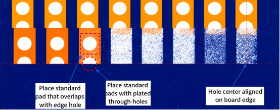
·The minimum diameter for half-holes should be 0.4mm to ensure compatibility with soldering processes.
·The annular rings around castellated holes should ideally measure at least 0.25 mm.
·The absolute minimum annular ring size is 0.18 mm to provide sufficient support.
Proper pad design is essential, as the pad must fully surround the hole, ensuring stability during soldering. Additionally, pads should be large enough to accommodate the entire solder fillet, maximizing solder joint reliability.
Creating the Board Outline
Accurately defining the board’s edge and shape is crucial for effective half cuts, as it ensures proper fit and alignment during assembly. While using solder pads and square pads to mount the module is an alternative to castellated holes, basically creating a precise board outline and pin layout is fundamental for the success of half cuts.
This involves accurately marking the board’s edge and shape to ensure seamless integration of the two boards during the assembly process and form.
Ensuring Proper Alignment and Spacing
Proper alignment and spacing are critical in the design of castellated holes and castellated pad. These holes offer the following benefits:
·Improve alignment during assembly
·Reduce the risk of misalignment issues
·Plated half-holes significantly lower the chances of alignment errors compared to pads under the module.
To ensure reliable connections and avoid assembly issues when working with castellated holes:
·Maintain consistent spacing of at least 0.5 mm between castellated holes.
·Design pads to accommodate the entire solder fillet.
·Include a small solder mask expansion around the pads to prevent bridging.
Manufacturing Process for PCB Half Cuts
The manufacturing process for PCB half cuts involves several specialized techniques to ensure precision and functionality. This process includes:
·Drilling and milling to create the half holes required for castellated edges
·Copper plating to enhance conductivity
·Solder mask application to protect the board
Quality control measures, including detailed inspections of the castellated edges, are essential to maintain the integrity and reliability of the PCB half cuts.
Drilling and Milling Process
Creating plated half-holes requires a detailed production process, which includes the following steps:
·Drilling
·Copper application
·Image transfer
·Pattern plating
·Film stripping
·Etching
·Solder mask printing
·Surface treatment
·Hole formation
·Contour milling
Specialized drilling equipment is crucial for this process, as any deficiencies can negatively impact subsequent steps. Heavy-duty milling bits and CNC machines are commonly used to achieve the required accuracy.
Modifying Gerbers to indicate drill hits and required plated holes plating is essential to ensure that the PCB with castellated holes passes fabrication.
Copper Plating and Solder Mask Application
Copper plating is a critical step in the production of plated half-holes and plated through hole, as it ensures reliable electrical connections. This process involves depositing a thin layer of copper on the PCB’s surface, enhancing conductivity for electronic components.
The solder mask application creates a barrier between the holes in a castellated hole array, acting as a solder dam. This not only protects the circuit pathways but also prevents solder bridging during assembly.
Quality Control and Inspection
Quality control procedures are vital to ensuring the integrity of the castellated edges. These procedures include visual inspections and automated optical inspections to confirm that the edges meet specified tolerances. Routine inspections are essential to detect any defects in the castellated edges, ensuring high reliability in PCB performance.
These measures guarantee that the manufacturing process achieves the desired precision and functionality.
Advantages of Using PCB Half Cuts
The use of PCB half cuts offers several advantages, making them an essential feature in modern PCB design. These include improved solder joints and connections, space-saving and compact designs, and versatility in assembly processes.
Modules using castellated holes can be easily replaced or upgraded, making them ideal for modular designs. Real-world applications demonstrate how PCB half hole cuts enhance module integration and assembly efficiency, ensuring that all components are covered effectively.
Improved Solder Joints and Connections
PCB half cuts improve solder joints and electrical connections by providing reliable mechanical strength on the PCB surface. The application of a solder mask protects the PCB from oxidation and ensures the integrity of the electrical connections.
These features enable robust board-to-board soldering, enhancing the overall performance of the circuit boards.
Space-Saving and Compact Designs
Half cuts in PCBs allow for a reduction in overall size, enabling more compact designs that fit into tighter spaces. This is particularly beneficial for devices with limited space, such as wearables and IoT gadgets.
PCB half cuts optimize layout by integrating additional components in tighter spaces without sacrificing functionality, ensuring that every other half of the design is utilized effectively.
Versatility in Assembly Processes
PCB half cuts offer unique flexibility, allowing for adaptable assembly options. They facilitate streamlined assembly processes by enabling surface mounting directly onto other PCBs. This versatility enhances the overall efficiency of the PCB assembly process, making it easier to integrate modules and achieve a seamless connection.
Practical Tips for Implementing PCB Half Cuts
Implementing PCB half cuts effectively involves following practical tips that ensure reliable connections and efficient designs. These tips include avoiding too much solder, selecting appropriate tools and software, and collaborating with PCB manufacturers.
Utilizing half cuts simplifies the assembly process by reducing misalignment risks and eliminating the need for additional connectors.
Avoiding Too Much Solder
Avoiding too much solder is crucial to ensure reliable connections during board-to-board soldering. The solder mask application defines the areas for soldering components on the PCB, protecting the copper and simplifying the solder application process.
Using calipers to measure the distance between the hole and the solder helps achieve optimal solder application and prevents issues such as bridging or misalignment.
Selecting Appropriate Tools and Software
Selecting the right tools and software is essential for designing PCB half cuts. The best PCB design tools allow easy creation of fabrication files, which is crucial for accurate manufacturing. Look for PCB design software that enables easy manipulation and visualization of castellated holes.
Effective tool selection streamlines the design process and contributes to the overall quality and functionality of the PCB.
Collaborating with PCB Manufacturers
Collaboration with PCB manufacturers is crucial for ensuring the accurate production of half cuts. The manufacturing process involves several steps, including precise drilling and milling to create half holes. Copper plating and solder mask application protect the integrity of the board, which is critical when creating castellated holes.
Quality control measures, including thorough inspection, ensure the characteristics of castellated edges are maintained.
Case Studies and Examples
Case studies provide practical insights into the benefits of implementing PCB half cuts in various projects. These examples showcase how castellated holes enhance connectivity and assembly efficiency in real-world applications.
Example 1: Wi-Fi Module Integration
Wi-Fi modules often utilize PCB half cuts to facilitate easier mounting and soldering to other circuit boards. This integration of integrated modules leads to increased efficiency, reduced assembly times, and improved reliability in performance with the pcb module.
Half cuts simplify assembly processes, ensuring reliable electrical connections in Wi-Fi modules.
Example 2: Small Module Assembly
Castellated holes are frequently utilized in small module assemblies to enhance connectivity. These holes enable streamlined board-to-board soldering, reducing the need for additional connectors and simplifying the assembly process, especially when using plated through holes and castellated vias.
This example illustrates how castellated holes provide reliable mechanical connections and improve overall assembly efficiency.
Summary
In conclusion, PCB half cuts and castellated holes are indispensable features in modern PCB design, offering improved solder joints, compact designs, and versatile assembly processes. By understanding their definition, applications, design considerations, and manufacturing processes, you can implement these features effectively in your projects. Embrace the potential of PCB half cuts to enhance your electronic designs and achieve seamless connections.
FAQs
Q.What are PCB half cuts and castellated holes?
A.PCB half cuts, also known as castellated holes, are partial cuts on a circuit board that facilitate board-to-board soldering connections, improving reliability and enabling more compact designs.
Q.What are common applications for castellated holes?
A.Castellated holes are primarily utilized for mounting PCB modules, such as Bluetooth and Wi-Fi, as they ensure robust soldered connections and simplify the assembly process. Their design enhances reliability and ease of integration in electronic applications.
Q.What are key design considerations for PCB half cuts?
A.Key design considerations for PCB half cuts include maintaining a minimum hole diameter of 0.4 mm, ensuring an annular ring of at least 0.25 mm, and designing pads to fully encompass the holes. These factors are crucial for reliable performance and manufacturability.
Q.How do you avoid using too much solder when implementing PCB half cuts?
A.To prevent excessive solder during PCB half cuts, it is essential to apply the appropriate volume of solder paste, utilize a solder mask for precise solder area definition, and accurately measure distances with calipers. This approach ensures optimal solder application and enhances board quality.
Q.Why is collaboration with PCB manufacturers important when implementing half cuts?
A.Collaboration with PCB manufacturers is crucial for ensuring accurate production and maintaining the integrity of castellated edges through precise drilling and milling, coupled with effective quality control measures. This partnership guarantees the successful implementation of half cuts
Author: Jack Wang

