


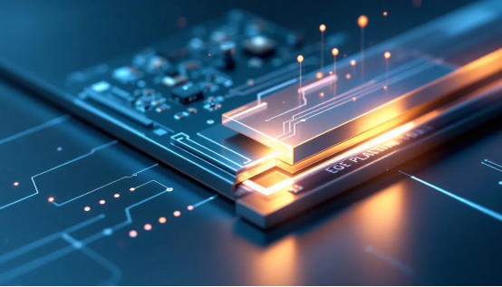
Mastering PCB Edge Plating: Top Tips for Effective Design
Introduction
Mastering PCB Edge Plating: Top Tips for Effective Design
PCB edge plating involves coating the edges of a printed circuit board with metal to improve conductivity, grounding, and durability. This article will cover its benefits, common materials used, application techniques, and key design considerations. Read on to understand how PCB edge plating enhances your circuit board’s performance and reliability.
Key Takeaways
·Edge plating enhances PCB performance by improving electrical connectivity, offering protection against electromagnetic interference (EMI), and increasing structural integrity.
·Key materials for edge plating include copper, gold, and nickel, each providing distinct advantages such as conductivity, corrosion resistance, and barrier protection.
·Effective design and communication with manufacturers are essential for successful edge plating implementation, including specifying plating thickness and ensuring proper documentation.
Understanding PCB Edge Plating
Edge plating, also known as called edge plating, metalized edge plating, side plating, or border plating, is a technique used to enhance the performance and reliability of printed circuit boards. This process involves coating the sidewalls of the PCB substrate with copper and a metallic coating, extending from the top to the bottom surface along the peripheral edges. This method is particularly advantageous for grounding or shielding against electromagnetic interference (EMI).
One of the primary reasons for utilizing edge plating is to improve conductivity and make edge connections more robust. It also serves to connect secondary PCBs to the main board and to facilitate soldering during assembly. Depending on the design requirements, edge plating can be applied to single-axis or multi-axis edges, making it a versatile solution for various PCB configurations.
Edge plating is not just limited to enhancing electrical connections; it also provides structural benefits. Coating the edges makes the PCB more resistant to lateral impacts and less prone to physical damage. Many designers consider edge plating essential for modern PCB design, ensuring both electrical and mechanical integrity of the circuit board.
Key Benefits of Edge Plating in PCBs
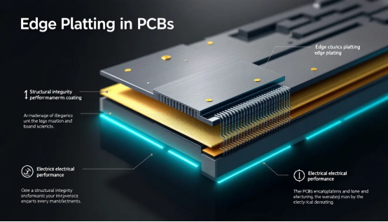
The advantages of edge plating in printed circuit boards are numerous, making it a highly valued technique in the PCB industry. One of the most significant benefits is its ability to serve as a barrier against electromagnetic interference (EMI). By providing a continuous conductive path along the PCB edges, edge plating enhances signal and power integrity, ensuring that your circuits function without unwanted interruptions.
Another critical benefit is the improved grounding for chassis signals. Edge plating offers enhanced chassis grounding, which is crucial for maintaining stable electrical connections and minimizing noise in the circuit, thereby improving electrical connectivity. This is particularly important in high-frequency applications where signal integrity is paramount.
Edge plating enhances not just electrical connections but also the structural rigidity of the edges of the pcb. Metal plating on the edges increases rigidity, making them less prone to bending or warping during assembly and operation. This structural reinforcement ensures that the PCBs can withstand physical stresses, contributing to the overall durability and reliability of the final product.
Common Materials for PCB Edge Plating
When it comes to edge plating materials, copper is the most commonly used due to its excellent electrical conductivity and cost-effectiveness. Copper plating ensures that the electrical connections along the PCB edges are stable and dependable. However, other materials are also used, each offering unique benefits:
·Gold
·Silver
·Tin
·Nickel
Gold, for instance, is preferred for its superior corrosion resistance and ability to enhance solderability. Immersion gold or immersion silver is often recommended to improve the quality and reliability of the connections.
Nickel is commonly used as a barrier thin layer to prevent copper from diffusing into other metals, ensuring the longevity of the plated edges.
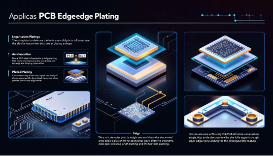
Techniques for Applying Edge Plating
Several techniques are employed to apply edge plating, each with its specific advantages. One common method involves creating an independent copper structure that is isolated from the main copper pour. This technique is particularly useful for creating a guard ring for chassis ground connection.
Another technique uses a polygon pour layer to define the edge plating in the PCB layout. This method extends the copper beyond the board edge, establishing a system ground connection that helps mitigate EMI and improves overall signal integrity. By carefully designing the copper pours, designers can ensure that the edge plating serves its intended purpose effectively, maintaining the outer contour and plated contour of the design.
In addition to these methods, it’s important to consider the specific requirements of your PCB design. The choice of technique will depend on factors such as the desired electrical performance, the physical layout of the PCB, and the specific application for which the PCB is intended. Understanding and applying these techniques ensures optimal results in your edge plating projects.
Design Considerations for Edge Plating
Designing for edge plating requires careful planning and attention to detail. One key consideration is extending the copper pour by about 0.5 mm over the edge of the PCB to ensure adequate coverage of the copper traces. This extension helps create a robust and reliable edge connection.
Clearance rules are crucial when designing for edge plating. Maintaining proper same clearance between the edge plating and any unconnected copper is vital to avoid short circuits. Polygon cutouts may be necessary around edge-mounted connectors when extending connected copper pours to prevent unintended electrical connections, especially in areas with exposed copper connections.
Removing the solder mask along the edge where plating is intended is another key consideration. This ensures proper metal contact and enhances the quality of the plating. Specifying the plating material and thickness in design documentation ensures compatibility with electrical and durability specifications. Adhering to these design rules ensures a successful and reliable edge plating implementation.
The Edge Plating Process
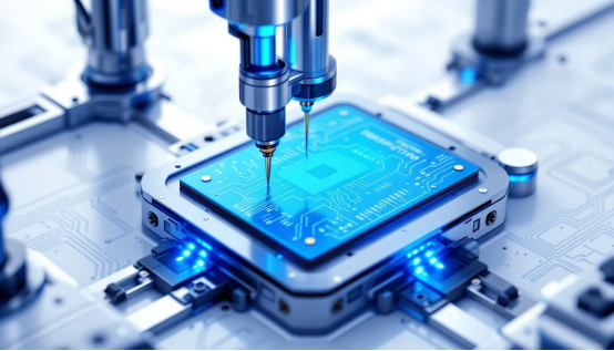
The edge plating process begins with the design phase, where the PCB layout is carefully planned to accommodate edge plating. Once the design is finalized, the surfaces of the PCB edges are cleaned and prepared to ensure proper adhesion of the plating.
The process of preparing a PCB for plating involves:
·Drilling holes to create access points for the through hole plating process.
·Milling metal slots prior to electroless copper plating to prepare the PCB edges for metallization.
·Applying electroless copper plating to form a conductive layer on the PCB edges before electroplating.
After the initial copper plating, additional layers such as nickel and gold may be applied to enhance solderability and protect the underlying metals from oxidation. A surface layer finish is typically applied to improve durability and solderability. The thickness of the plating is critical, with typical values around 100 micro-inches to ensure proper electrical performance.
Applications of PCB Edge Plating
PCB edge plating is widely used in various applications, particularly in RF PCB design. In RF PCB applications, edge plating helps create a ground connection to shielded enclosures and contains electromagnetic fields, enhancing signal integrity.
Edge plating also serves as a guard ring around the PCB, protecting sensitive components from external noise in RF designs and providing emi shielding at all four edges of the plate. This is especially important in high-frequency circuits, where minimizing interference and signal loss is crucial for maintaining performance.
Edge plating enhances the electrical performance of high-frequency circuits by providing a robust chassis ground. This ensures that the circuits function reliably and efficiently, making edge plating an essential technique in the design of modern electronic devices.
Using CAD Software for Edge Plating Design
Using CAD software for edge plating design is essential for achieving precision and quality in PCB layouts. Tools such as Cadence AWR and Altium 365 are invaluable for designing edge plating. These tools allow for simulations that integrate EMI mitigation strategies within PCB designs, enhancing the overall performance of the final product.
Modern CAD tools also enhance organizational aspects with hierarchical schematic design, making the management of complex projects easier. Collaborative features in these tools allow team members to work together seamlessly on PCB designs, ensuring that all aspects of the design are optimized for edge plating and include various technical features.
Leveraging CAD software capabilities allows designers to achieve higher levels of precision and efficiency in their edge plating projects. This ensures that the final PCB layout meets all the necessary specifications and performs reliably in its intended application.
Communicating Edge Plating Requirements to Manufacturers
Effective communication with manufacturers is crucial for ensuring that edge plating requirements and required specifications are met accurately. Including precise specifications for edge plating in fabrication drawings can prevent misunderstandings during fabrication. A specific note such as ‘PLATING TO BE ALONG BOARD EDGE’ is essential for clear communication.
When completing a quote form for PCB orders, it’s important to:
·Mention edge plating to eliminate any ambiguity about the design specifications.
·Clearly define the finished thickness of edge plating.
·Specify a range for the edge plating thickness to help manufacturers understand the exact requirements.
Including a checklist of edge plating requirements in your design files can streamline communication with the manufacturer and minimize errors. CAD software can facilitate the generation of essential manufacturing documents directly from pcb manufacturing layouts, ensuring that all relevant information is conveyed accurately.
Potential Challenges and Limitations
Despite its many benefits, edge plating has its challenges and limitations:
·The edge plating process cannot cover the entire edge length due to the fixation requirements of circuit boards during production.
·This requires careful layout planning.
·It may restrict V-cutting scores.
Copper peeling may occur if the plating does not achieve sufficient adhesion to the substrate surface, impacting the reliability of the edge plating. Burr formation during machining, especially on castellation holes, can also hinder the quality of edge plating and necessitates special handling to ensure success.
Discussing edge plating tolerances and capabilities with the manufacturer can help avoid costly redesigns, production errors, and equipment failures. By addressing these challenges proactively, designers can ensure that their edge plating implementations are both effective and reliable.
Summary
Mastering PCB edge plating is essential for creating high-performance and reliable printed circuit boards. From understanding the basics and benefits to selecting the right materials and techniques, each step in the edge plating process contributes to the overall quality of the final product.
By effectively communicating edge plating requirements to manufacturers and addressing potential challenges, designers can achieve optimal results in their PCB projects. With the right knowledge and tools, you can ensure that your PCBs are both structurally sound and electrically superior, paving the way for innovative and robust electronic designs.
FAQs
Q.What is PCB edge plating?
A.PCB edge plating involves the application of a copper layer to the sidewalls of a printed circuit board, which significantly improves its performance and reliability.
Q.What are the benefits of edge plating in PCBs?
A.Edge plating in PCBs enhances EMI shielding, ensures improved grounding, and increases structural integrity, ultimately leading to more reliable connections. This results in a more robust and efficient electronic design.
Q.What materials are commonly used for edge plating?
A.Copper, gold, silver, tin, and nickel are commonly used materials for edge plating, with copper being the most prevalent choice.
Q.What techniques are used for applying edge plating?
A.Edge plating techniques involve creating an independent copper structure and utilizing a polygon pour to accurately define the edge plating in the PCB layout.
Q.How can I communicate edge plating requirements to manufacturers?
A.To effectively communicate edge plating requirements to manufacturers, include precise specifications in fabrication drawings, clearly mention edge plating in quotes, and utilize checklists to ensure thorough understanding. This approach will facilitate clarity and precision in the manufacturing process.
Author: Jack Wang

