IC Packaging Substrate Technology for Engineers: A Comprehensive Guide
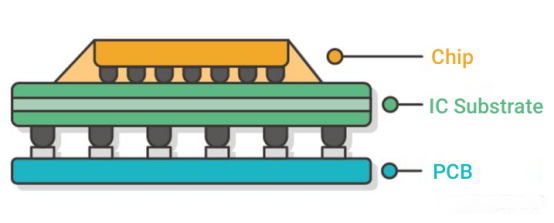
In the wave of upgrades towards higher density and miniaturization in the electronics industry, the performance of integrated circuits (ICs) relies heavily on the support of the packaging process. As a critical interface between the bare chip (DIE) and the printed circuit board (PCB), the IC packaging substrate serves as the "high-end skeleton" of semiconductor packaging. Also known as the IC package substrate, it is a high-end class of PCBs developed based on high-density interconnection (HDI) technology. With its characteristics of high density, high precision, and a large number of pins, it has completely replaced traditional lead frames in the mid-to-high-end packaging field, providing essential support for the miniaturization, high performance, and high reliability of electronic devices.
IC Packaging Substrates: The Core 'Bridge' of Semiconductor Packaging
IC packaging substrates play a critical role in semiconductor packaging, serving as the essential bridge that supports and connects the chip to the external circuit, with a wide range of core functions including physical protection, signal conduction, and multi-functional integration.
Core Functions: Threefold Value as a Critical Link
• Physical Support and Protection: Provides stable support for bare chips, shielding them from external disturbances such as humidity and vibration, and is especially suited for packaging microchips smaller than 2mm × 2mm. For example, the ceramic-based IC substrate customized by Jianxiangsheng for a MEMS sensor customer successfully solved the problem of securing microchips.
• Precise Signal Transmission: Achieves interference-free connections between the chip and external circuits through ultra-fine trace designs, accommodating high-pin-count, high-end chips. Jianxiangsheng's ABF film IC substrates meet the signal transmission demands of high-end CPUs and effectively prevent signal crosstalk.
• Multi-functional Integration: Integrates multiple functions such as heat dissipation, resistance to extreme environments, and modular interconnection. In automotive-grade chip packaging, the custom substrates can withstand temperature fluctuations ranging from -40°C to 125°C, while also offering vibration resistance and moisture protection.
Explanation of Key Industry Terms
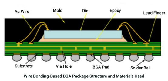
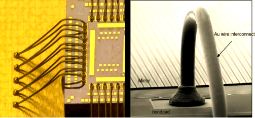
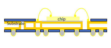
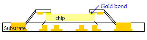
- W/B (Wire Bonding): A technique that uses gold or aluminum wire and thermal ultrasonic pressure to connect the chip to the substrate, commonly used in RF, storage, and other modules.
In IC packaging, the method of circuit connection is crucial. Among the main techniques are flip-chip bonding, tape automated bonding, and wire bonding.
Wire bonding refers to the process of connecting the chip to the package substrate or lead frame using circuit connections, ensuring smooth transmission of electronic signals. Wire bonding technology can be classified into different types based on the process. It includes ball bonding and wedge bonding. Ball bonding relies on high temperature and high pressure, while wedge bonding focuses on a specific angle during the welding process. Additionally, based on the bonding principles, wire bonding can be further divided into thermocompression bonding, ultrasonic bonding, and thermosonic bonding. These three methods differ in temperature, ultrasound use, and required pressure, and are suitable for various wire materials such as gold (Au) and aluminum (Al).
The principle of thermosonic bonding involves simultaneously applying heat and ultrasonic energy to the metal wire and the bonding point. During this process, the contact surface undergoes plastic deformation, and the oxide layer on the interface is broken, activating it. Then, through diffusion between the metals on both sides of the contact surface, the connection is completed.
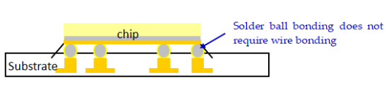
- FC (Flip Chip Bonding): The chip is flipped and directly connected to the substrate using solder bump pads, offering higher signal density and making it suitable for high-end chips like CPUs and GPUs.
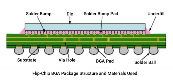
- BGA (Ball Grid Array): A packaging type with a solder ball array on the bottom for connections, offering excellent heat dissipation and electrical performance. It is the mainstream packaging form for PC and server-level processors.
- CSP (Chip Scale Packaging): The packaging area is no more than 1.2 times the size of the bare chip, making it suitable for the demand for thinner and more compact mobile devices.
Core Materials: The 'Performance Foundation' of IC Substrates
Materials are the "framework" of IC substrates, directly determining the performance potential of the product. PCBMASTER carefully selects top-tier global brand materials, with each material undergoing multiple rounds of performance testing to ensure quality control from the source, precisely adapting to the needs of different packaging scenarios.
BT Material (Bismaleimide Triazine)
BT, short for Bismaleimide Triazine, is a high-performance epoxy resin substrate that outperforms FR4. It is synthesized from triazine and bismaleimide and is the preferred laminate material for many manufacturers. It offers advantages such as a high glass transition temperature, excellent insulation properties, low coefficient of thermal expansion, and a low dielectric constant. BT material is the standard substrate for BGA packaging and is also suitable for CSP packaging. It is heat-resistant, has low dielectric loss, and is highly machinable, making it widely used in component packaging for fields like communications and computing.
ABF Material (Ajinomoto Buildup Film)
ABF material (Ajinomoto Buildup Film) is the "top performer" in high-end substrates, with a low dielectric constant, low dielectric loss, and excellent dimensional stability. It is custom-designed for ultra-fine traces and ultra-high-density packaging, making it the material of choice for advanced packaging of AI chips, server chips, and other high-end applications.
Ceramic Material
Ceramic material is known for its exceptional thermal conductivity, with a thermal conductivity coefficient as high as 200W/(m·K). It is suitable for automotive-grade SiC modules and aerospace products, capable of withstanding extreme environmental conditions.
Mitsubishi Material
Mitsubishi material represents the "steady" choice, with an extremely low coefficient of thermal expansion and excellent dimensional stability. Even after multiple lamination and high-temperature processing, it resists expansion and contraction, offering outstanding electrical insulation. It provides a solid foundation for high-density circuit layouts.
Doosan Material
Doosan material is the "signal transmission expert," with a low and stable dielectric constant, resulting in minimal signal loss. It is ideal for high-frequency, high-speed chip applications, featuring excellent mechanical toughness and strong impact resistance, enhancing the durability of the substrate.
Toshiba Material
Toshiba material offers both heat resistance and heat dissipation advantages, it quickly disperses localized heat from the chip. With a mature manufacturing process, it can precisely meet the stringent requirements for fine circuitry and micro-hole fabrication.
LG Material
LG material is the "all-rounder," with balanced electrical and mechanical properties. It features low dielectric loss and high mechanical strength, seamlessly integrating with various surface treatment processes. It is suitable for packaging components with medium to low contact density.
Guangdong Yinghua Substrate BT Material
Guangdong Yinghua Substrate BT material is the "rising star" with an unbeatable cost-performance ratio. It offers low expansion and shrinkage, effectively solving warping issues. With a Tg value of 260°C and a delamination time of over 60 minutes at 288°C, it withstands thermal shock for more than 300 seconds. At 1GHz, its dielectric constant is just 4.3, with a dielectric loss of 0.008, providing excellent insulation and signal transmission capabilities. It is suitable for various packaging scenarios, including CSP, BGA, and FC-PKG.
Key Differences Between IC Packaging Substrates and Traditional PCBs
Many customers tend to equate IC packaging substrates with "high-end PCBs," but there are fundamental differences between the two in terms of materials, precision, functionality, and more. Based on practical experience, PCBMASTER provides a comparative analysis across six core dimensions:
| Comparison Dimensions | IC Packaging Substrate | Traditional PCB |
| Core Materials | BT Resin, ABF Film, Ceramic, PI Flexible Substrate, and others | Primarily FR-4 Glass Fiber Substrate |
| Line Width/Line Spacing Precision | Mass production at 15μm/15μm, custom designs can achieve below 10μm | Standard above 50μm, precision models with a minimum of 30μm |
| Manufacturing Process | MSAP Improved Semi-additive Process, LDI Laser Direct Imaging Exposure | Traditional Subtractive/Additive Process, Sampling Inspection |
| Pin Load Capacity | Thousands of pins (suitable for BGA/CSP packaging), up to 60,000 pins | Hundreds to thousands of pins (suitable for QFP packaging), up to 5,000 pins |
| Core Functionality | Chip-level interconnect, supporting multi-layer vertical interconnection (suitable for Chiplets) | Basic connection from the component to the motherboard |
| Typical Application Scenarios | CPU/GPU, Automotive-grade SiC Modules, MEMS Sensors, High-end Storage | Computer Motherboard, Mobile Phone Motherboard, Home Appliance Control Board |
Product System: Customized Solutions for Diverse Scenarios
Leveraging its extensive material resources and process capabilities, PCBMASTER has built a comprehensive IC packaging substrate product system, classified by connection technology and packaging type, to precisely match the differentiated packaging needs of various electronic devices.
Classified by Chip-to-Substrate Connection Technology
- W/B Substrate: Utilizes gold/aluminum wire thermal ultrasonic bonding, suitable for RF modules, storage chips, and more. The minimum pitch/width of the bonding fingers reaches 95μm/35μm (sample specifications).
- FC Substrate: Direct connection using solder bump pads, offering high signal transmission efficiency. Suitable for high-end chips like CPUs and GPUs. The FCBGA model uses ABF resin substrate and supports a 4-layer HDI stacked via structure.
- TAB Substrate: Gold-to-gold thermocompression bonding, suitable for specific high-precision applications.
Classified by Packaging Type
- PBGA Substrate (Plastic Ball Grid Array Substrate): A "reliable partner" for components with medium to low contact density. It uses wire bonding technology and pairs with materials like BT and Yinghua, offering excellent cost performance. It is widely used in computers and communication products.
- FCBGA Substrate (Flip-Chip Ball Grid Array Substrate): The "performance leader" for high-speed computing and high-contact-density components. It uses premium materials such as ABF and Mitsubishi, supporting massive data transmission. It is suitable for AI servers and high-end computers.
- CSP/FCCSP Substrate: The "pioneer of thin and light" in consumer electronics. FCCSP focuses on fine-pitch requirements, while CSP has a packaging area no larger than 1.2 times the chip area, with board thickness as low as 0.1mm. It is suitable for mobile AP/baseband chips.
- SiP Substrate (System-in-Package Substrate): The "space optimization master" for portable devices. With high integration and compact size, it relies on low-power, high-stability materials to help smartphones and smartwatches achieve thin form factors and long battery life.
- Memory Card Substrate (MCP Substrate): The "data transmission guardian" for storage devices. It is compatible with memory cards, smartphones, servers, and more, ensuring fast data reading and stable transmission.
- LGA Substrate (Land Grid Array Substrate): The "high-frequency pioneer" for high-end devices. It is suitable for high-frequency, high-power, and high-density I/O applications, using high-temperature-resistant, low-loss materials to support performance breakthroughs in premium products.
Core Technology System and Production Process
IC packaging substrate technology has extremely high barriers to entry. PCBMASTER leverages advanced equipment, mature processes, and full-process quality control to achieve independent control over key technologies, creating a standardized "quality assurance line."
Comprehensive Analysis of Core Manufacturing Processes
- Substrate Preparation: High-end materials such as Shengyi, BT, Mitsubishi, and ABF are selected. The substrates undergo cutting, edge rounding, washing, and drying processes, with strict control over warping. For automotive-grade products, Tg180°C-220°C BT resin substrates are exclusively used.
- Inner Layer Fabrication: The circuit is formed through the process of "degreasing, micro-etching, acid cleaning, film lamination, exposure, and DES etching." The micro-etching depth is controlled between 0.5 to 1.5 microns to ensure strong adhesion between the circuitry and the substrate.
- Lamination Process: Hot pressing at 200-220°C and 2.45 MPa, combined with precise cooling control, to prevent board warping and resin overflow. The interlayer alignment deviation is kept to ≤12μm, exceeding IPC-6012 Class 3 standards by 30%.
- Fine Line and Micro-hole Processing: Using the SAP/MSAP semi-additive process to achieve stable mass production of 15μm/15μm lines, with edge saw-tooth control within ±1μm. High-precision laser drills are capable of creating 0.05mm micro-holes with a hole diameter tolerance of ±5μm.
- Surface Treatment: Supports processes such as hard gold, soft gold, ENEPIG-WB, ENEPIG-SMT, and OSP. The hard gold Ni layer is 5-15μm, with a gold layer of 0.2-0.5μm, meeting high-reliability soldering requirements.
Standardized Production Process
PCBMASTER’s standardized production process ensures seamless quality and consistency at every stage.
Copper Foil Substrate Preparation → Inner Layer Fabrication → Lamination/Stacking → Laser Drilling/Mechanical Drilling → Through-hole/Plug-hole Plating → Outer Layer Fabrication → Solder Mask Printing → Surface Treatment → Outline Cutting → ET Electrical Performance Testing → FQC Full Inspection (180x CCD Detection) → Finished Product Shipping.
Core Technical Challenges and Solutions
Technical Challenge PCBMASTER's Solution Application Results Warping and Shrinkage of Ultra-thin Substrate Optimized lamination structure and pressing parameters, upgraded positioning reference technology Flatness error of 0.1mm ultra-thin board ≤ 5μm Interlayer Alignment Deviation LDI alignment exposure + multiple stacking calibration Interlayer alignment deviation of 8-layer board ≤ 12μm Solder Mask Hole Planarity Customized solder mask ink + precise printing control Solder mask thickness 20±5μm, planarity ≤ 5μm Pad Planarity of Surface Treatment Optimized plating parameters, using crystallization refinement technology ENEPIG process pad planarity error ≤ 2μm Detection of Micro Defects Full-process online AOI + specialized flying probe tester Defect detection rate 100%, sample yield ≥ 98%
Core Technical Parameters: The 'Quantified Representation' of Hard Power
PCBMASTER's IC substrate core parameters reach industry-leading standards, capable of meeting the product requirements of varying complexities and precision. The specific specifications are as follows:
| Project | Mass Production Specifications | Sample Specifications |
| Number of Layers | 2-10 layers | 2-12 layers |
| Minimum Drilled Hole Diameter | 50μm | 50μm |
| Bonding Finger Minimum Pitch/Width | 105μm/35μm | 95μm/35μm |
| Minimum Line Width/Spacing | 25μm/25μm | 25μm/25μm (customizable to 10μm) |
| Minimum Soldering Ring | 80μm | 80μm |
| Minimum Board Thickness (2L/4L/6L/10L) | 100μm/300μm/400μm/800μm | 100μm/200μm/300μm/800μm |
| Line to Pad/Board Edge Distance | 100μm | 75μm |
| Solder Mask Dam/Pad/Thickness | 50μm/80μm/20±5μm | 50μm/70μm/20±5μm |
| Flatness | 5μm | 5μm |
Additional Key Performance Parameters
- Board Thickness Range: 0.1 to 1.2mm, tolerance ±30μm; Unit size ≤ 150×150mm, size tolerance as small as ±50μm.
- Hole Diameter Range: 30 to 150μm, with each unit capable of supporting hundreds to thousands of micro-holes; minimum BGA pad diameter is 50μm.
- Interconnection Technology: Supports via-in-via, blind vias, and stacked via technologies.
PCBMASTER: A Professional Service Provider in the IC Substrate Field
With over a decade of technical expertise in the IC packaging substrate sector, PCBMASTER fully implements ISO9001, IATF16949, ISO13485 aerospace-grade quality management systems and ROHS environmental standards. We have a dedicated R&D team of over 20 professionals, providing customers with one-stop services from material selection and solution design to custom manufacturing.
Core Service Advantages
- Fast Response and Delivery: We maintain a variety of substrate brands in stock, with sample delivery times ranging from 12 to 30 days. For a Chiplet project, substrate matching was completed in 7 days, and the first batch of samples was delivered in 20 days, helping customers shorten development cycles.
- Strict Quality Control: Equipped with advanced equipment such as LDI exposure machines, high-precision laser drills, and full-process online AOI, all samples undergo 100% full inspection with flying probe testers before shipment. Our yield rate remains stable at over 98%.
- Customization Capabilities: We offer tailored substrates and processes for automotive, aerospace, and high-end computing applications. For example, a substrate for a new energy vehicle’s SiC module passed 1000 thermal shock cycles between -40°C and 125°C, with a lifespan exceeding 120,000 hours.
Conclusion
IC substrates play a crucial role in the performance and reliability of modern electronic devices. With years of expertise and a commitment to innovation, PCBMASTER delivers high-quality, customized solutions that meet the demanding requirements of various industries, including automotive, aerospace, and high-end computing. Our focus on precision, quality control, and fast delivery ensures that our substrates continue to support the advancements in technology.
FAQs
1. What is an IC substrate and why is it important in semiconductor packaging?
An IC substrate is a key component in semiconductor packaging that connects the chip to external circuits. It provides mechanical support, electrical connections, and helps with heat dissipation, all of which are essential for the performance and reliability of modern electronic devices.
2. What are the key factors that determine the quality of an IC substrate?
The quality of an IC substrate is determined by several factors, including material selection, layer structure, precise interlayer alignment, and the ability to support fine-pitch and high-density interconnects. Advanced manufacturing processes, such as laser drilling and automated optical inspection (AOI), also play a critical role in ensuring high-quality substrates.
3. How do IC substrates support high-performance applications like AI chips or automotive systems?
IC substrates are designed to handle high-density connections, heat dissipation, and extreme operating conditions. For AI chips, they support fine interconnects for fast data transmission, while for automotive systems, they need to withstand harsh temperatures and mechanical stresses. The ability to customize materials and processes ensures that substrates meet the specific requirements of these demanding applications.
4. What are the most common challenges in IC substrate manufacturing?
Common challenges in IC substrate manufacturing include managing warping and shrinkage of ultra-thin substrates, ensuring precise alignment between layers, and maintaining consistency in solder mask thickness. Additionally, achieving high precision in micro-hole drilling and fine-pitch interconnects can be difficult, especially for advanced packaging designs.
5. How does the choice of material impact the performance of an IC substrate?
The choice of material significantly affects the performance of an IC substrate. For example, materials like BT resin offer good thermal stability, while ABF film is ideal for high-density interconnects. Ceramic materials are used for their excellent heat dissipation properties, while flexible substrates, such as PI, are used for applications requiring flexibility and durability.
Author Bio
Hi, I'm Carol, the Overseas Marketing Manager at PCBMASTER, where I focus on expanding international markets and researching PCB and PCBA solutions. Since 2020, I've been deeply involved in helping our company collaborate with global clients, addressing their technical and production needs in the PCB and PCBA sectors. Over these years, I've gained extensive experience and developed a deeper understanding of industry trends, challenges, and technological innovations.
Outside of work, I'm passionate about writing and enjoy sharing industry insights, market developments, and practical tips through my blog. I hope my posts can help you better understand the PCB and PCBA industries and maybe even offer some valuable takeaways. Of course, if you have any thoughts or questions, feel free to leave a comment below—I'd love to hear from you and discuss further!