


What Are HDI PCBs? Key Features, and When to Use Them
As electronics become smaller and more powerful, the need for circuit boards that can pack advanced features into tight spaces is growing. Market reports show that the global HDI PCB market is expected to grow from USD 19.59 billion in 2025 to USD 34.23 billion by 2032, with a CAGR of 8.3%.
HDI PCBs solve the problem of fitting high-performance electronics into tiny devices. They use advanced techniques like microvias, fine traces, and high pad density to deliver more connections in less space. This technology is essential for creating 5G devices, IoT sensors, and wearables that need to be compact but still operate at peak performance. As demand for smaller, faster, and smarter electronics continues to rise, HDI PCBs are becoming more crucial to driving innovation in almost every tech sector.
What Are HDI PCBs?
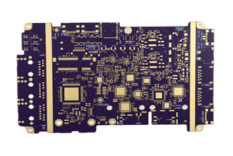
HDI PCBs (High-Density Interconnect Printed Circuit Boards) are advanced circuit boards designed to support high-performance electronics in compact spaces. Unlike traditional PCBs, which use larger vias and wider traces, HDI PCBs incorporate smaller, more precise connections to fit more functionality into a reduced area. This makes HDI PCBs essential for modern electronics that require both miniaturization and high-speed performance.
These boards utilize microvias, fine traces, and high-density connections to reduce space while improving signal integrity and performance. HDI PCBs are commonly used in devices like smartphones, medical wearables, and automotive electronics, where performance and size are both critical factors.
What Are the Key Features That Set HDI PCBs Apart?
HDI PCBs stand out due to their advanced features like microvias, fine traces, high pad density, and low signal loss. These features enable more components to fit into smaller spaces, making them ideal for compact, high-performance devices such as smartphones, wearables, and automotive electronics. HDI PCBs offer improved signal integrity and efficiency, allowing for faster data processing and more reliable performance in space-constrained applications.
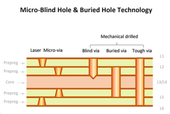
Via Technology: Microvias, Blind Vias, and Buried Vias
Microvias, blind vias, and buried vias are advanced types of vias used in HDI PCBs. Vias are tiny holes used to connect different layers of the PCB. These specialized vias offer significant advantages in terms of space efficiency and signal integrity.
Microvias: These are the smallest vias (less than 150μm in diameter) and are created using laser drilling. Microvias save valuable space on the PCB, allowing for more compact designs. For example, in smartphones, microvias enable high-density connections between different layers while keeping the board thin.
Blind Vias: These connect the outer layers to one or more inner layers but do not go all the way through the PCB. They help save space and reduce board thickness, critical for wearable devices that need to be lightweight yet powerful.
Buried Vias: These vias connect only the inner layers and are hidden from the outer layers of the PCB. They enable the creation of dense, multi-layered circuit boards that support complex components, such as in automotive ADAS (Advanced Driver Assistance Systems).
Real-World Impact: In smartphones, these via technologies allow manufacturers to pack more components into a smaller space without compromising performance. In wearables, the small size and efficient connections enable compact designs without sacrificing features. For automotive electronics, buried and blind vias allow the inclusion of complex circuits for features like LiDAR or radar systems in tight spaces.
Trace and Space: Fine Traces for High-Density Circuits
HDI PCBs use fine traces and narrow spaces to route electrical signals more efficiently. Trace widths can be as small as 0.1mm (4 mils), compared to the standard 0.2mm (8 mils) in traditional PCBs. This smaller trace width allows more components to be placed in the same area, which is crucial for high-performance devices.
Trace width plays a key role in reducing the size of the PCB and enabling high-speed signal routing. In devices like 5G smartphones and IoT sensors, the ability to route signals efficiently with minimal signal degradation is critical. The fine traces in HDI PCBs reduce signal loss and minimize interference, ensuring faster and more reliable data transmission.
Example: In 5G devices, fine traces enable the efficient routing of high-frequency signals without signal loss, which is essential for 5G's fast data speeds. Similarly, in IoT devices, fine traces ensure that complex circuits with multiple sensors can operate simultaneously without interference.
Real-World Impact: By using fine traces, manufacturers can create smaller, more powerful circuits for wearables like fitness trackers, where space is limited but the device needs to handle complex sensor data. For 5G applications, these fine traces allow the board to handle high-frequency signals efficiently, ensuring devices maintain optimal performance.
Pad Density: Supporting High-Pin Components in Small Spaces
Pad density refers to the number of pads (connection points for components) per square centimeter on a PCB. In HDI PCBs, pad density is typically greater than 50 pads/cm², allowing manufacturers to pack more components into a smaller area. This is especially important for modern high-pin components, such as BGAs (Ball Grid Arrays), which have hundreds of tiny pins that must be connected to the PCB.
Understanding Pad Density: High pad density enables the use of BGAs with a 0.4mm pitch or smaller, which is common in advanced processors and memory chips. This allows manufacturers to include powerful chips in smaller, more compact devices.
Real-World Benefits: In devices like smartphones, laptops, and automotive electronics, the ability to support high-pin components allows for more powerful processors and more features, all while keeping the device compact. This is essential for devices where performance cannot be compromised due to size constraints.
Real-World Impact: For smartphones, HDI PCBs with high pad density support advanced chips like Qualcomm’s Snapdragon processors, enabling complex functionalities like AI processing, gaming, and high-speed connectivity in a small form factor. In automotive electronics, high pad density supports components in ADAS systems, where multiple sensors and processors are needed for real-time decision-making.
Electrical Performance: Low Signal Loss and Controlled Impedance
One of the most crucial aspects of HDI PCBs is their ability to provide low signal loss and controlled impedance, which are essential for high-speed, high-frequency devices. As devices like 5G smartphones, medical equipment, and automotive systems require fast data processing and real-time communication, maintaining the quality of the electrical signal is critical.
Signal Integrity: HDI PCBs are designed with controlled impedance, ensuring that signals travel smoothly and without interference, even at high speeds. This is important for devices that handle large volumes of data, such as 5G and IoT applications.
Reduced Signal Loss: The fine traces and compact design of HDI PCBs result in shorter trace lengths and less resistance, which minimizes signal loss. This makes HDI PCBs particularly valuable in devices that rely on high-speed communication and precision, such as wearables and medical monitoring devices.
Real-World Impact: In 5G networks, HDI PCBs help maintain signal integrity even at frequencies as high as 60GHz, ensuring smooth data transmission and minimal interference. In medical wearables, such as continuous glucose monitors, HDI PCBs ensure that the device can transmit accurate data in real-time, providing reliable monitoring for patients.
How Do HDI PCBs Differ From Standard PCBs in Performance?
HDI PCBs offer several performance advantages over traditional standard PCBs, especially in compact, high-performance applications. Their design features enable better space efficiency, improved signal integrity, and superior electrical performance. Let's break down these differences in key areas:
Size and Space Efficiency
HDI PCBs are significantly more space-efficient than standard PCBs, making them ideal for devices where size reduction is crucial.
Microvias and Fine Traces: The use of microvias (tiny holes less than 150μm in diameter) and fine traces (as small as 0.1mm) allows for more compact circuit layouts. Microvias take up less space than traditional through-hole vias, which are larger and need more area for placement.
Impact on Device Size: Due to the smaller traces and microvias, HDI PCBs can fit more components into smaller spaces, making devices 30–50% smaller than those using standard PCBs. This is especially beneficial for devices like smartphones, wearables, and medical devices, where space is limited but performance cannot be compromised.
Example: A smartphone motherboard using HDI PCB technology can be much thinner and lighter while still supporting high-performance components like 5G chips or high-resolution displays, which would be difficult with standard PCB designs.
Signal Integrity and Speed
HDI PCBs are designed to improve signal integrity and support high-speed signals, making them the go-to choice for modern, high-performance applications.
Low Signal Loss: HDI PCBs minimize signal loss due to their fine traces and shorter routing paths. This is particularly important in high-frequency applications like 5G and IoT devices, where every millisecond counts. The compact design reduces the resistance and capacitance that cause signal degradation in longer or wider traces.
Controlled Impedance: HDI PCBs are also designed with controlled impedance, ensuring that signals maintain their integrity as they travel through the PCB. This helps prevent signal reflections and distortions, which can result in data loss or slower processing speeds.
High-Speed Capabilities: HDI PCBs are essential for devices that need to transmit data quickly and reliably. This includes 5G networks, high-speed routers, and automotive radar systems, all of which require minimal delay and precise signal transmission.
Example: In 5G smartphones, HDI PCBs help manage high-frequency signals that can reach speeds of 6 GHz or higher, ensuring fast data transfer with minimal interference. For IoT sensors, HDI PCBs enable quick data processing and communication in devices like smart thermostats, wearables, and fitness trackers.
Electrical Performance
HDI PCBs offer better electrical performance compared to standard PCBs, particularly when it comes to power handling and heat dissipation.
Improved Power Handling: HDI PCBs use thicker copper layers in certain regions, allowing for better power distribution. This is particularly useful in power-hungry applications, such as electric vehicle (EV) battery management systems (BMS) or high-power LEDs, where the PCB must handle higher currents.
Heat Dissipation: The dense copper layers and optimized ground planes in HDI PCBs help with heat dissipation. Efficient heat management prevents components from overheating, which could otherwise reduce device lifespan or cause malfunction.
Example: In automotive electronics, HDI PCBs are used in EV battery management systems where they must handle high currents and manage heat efficiently to ensure safe and reliable operation. Similarly, in medical devices like portable ultrasound machines, heat management is crucial for maintaining consistent performance.
Comparison Table: HDI vs. Standard PCBs
| Feature | HDI PCB | Standard PCB |
| Via Technology | Microvias, Blind Vias, Buried Vias | Through-hole Vias |
| Trace Width | 0.1mm or smaller | 0.2mm or larger |
| Signal Integrity | Low signal loss, controlled impedance | Higher signal loss at high speeds |
| Device Size | 30-50% smaller than standard PCBs | Larger, bulkier designs |
| Electrical Performance | Better power handling and heat dissipation | Lower power handling capacity and less efficient heat dissipation |
| Applications | Smartphones, Wearables, 5G, IoT | Basic consumer electronics |
Why Are HDI PCBs Essential for Modern Electronics?
HDI PCBs are crucial for the advancement of modern electronics. They support the growing demand for smaller, faster, and more powerful devices, enabling cutting-edge technologies like 5G, AI, and IoT. Their compact design and high functionality make them indispensable in industries ranging from consumer electronics to aerospace. Let’s dive into why HDI PCBs are essential for modern tech.
Supporting the Demands of Modern Technology
HDI PCBs are at the heart of the technological revolution, providing the necessary infrastructure for devices that demand high performance in small spaces.
Enabling 5G, AI, and IoT Technologies: As demand for 5G connectivity, AI-powered devices, and IoT systems grows, HDI PCBs offer the compactness and high-speed signal integrity required. For example, 5G networks use HDI PCBs to handle high-frequency signals at speeds exceeding 6GHz, ensuring low latency and high data throughput. Without the efficiency of HDI PCBs, devices like smartphones, smart cities, and autonomous vehicles would struggle to keep up with the ever-increasing data demands.
Powering Compact, High-Performance Devices: HDI PCBs enable the miniaturization of electronic circuits, crucial for products like smartphones, wearables, and fitness trackers. These devices require efficient use of space without sacrificing performance. Smartphones, for instance, use HDI PCBs to support 5G capabilities, AI processors, and high-resolution displays in slim, lightweight designs. The ability to pack more functionality into smaller spaces allows users to enjoy a powerful computing experience in the palm of their hands.
Compact Design & High Functionality
One of the key reasons HDI PCBs are so important for modern electronics is their ability to combine compact design with high functionality, meeting the requirements of next-gen technologies.
Importance of HDI PCBs for Miniaturized Devices: As technology becomes more integrated into our daily lives, the demand for smaller devices continues to grow. HDI PCBs provide the ideal solution by supporting dense, high-performance circuits in a compact format. For example, a wearable fitness tracker needs to fit into a tiny, comfortable wristband while offering sensors, communication features, and long battery life. HDI PCBs allow for such miniaturization without compromising performance or reliability.
Applications in Multiple Industries: HDI PCBs are used across a wide range of industries, each requiring unique performance attributes from their circuit boards. Here are some key sectors where HDI PCBs play an essential role:
- Consumer Electronics: From smartphones to laptops, HDI PCBs enable the development of slimmer and more powerful devices with the latest features, such as 5G and high-resolution cameras.
- Medical Devices: Devices like wearable health monitors, portable ultrasound machines, and glucose sensors rely on HDI PCBs for their compact, reliable performance in critical health applications.
- Automotive: Electric vehicles (EVs), ADAS (Advanced Driver-Assistance Systems), and autonomous cars use HDI PCBs to manage high-speed data processing and sensor integration in space-constrained environments.
- Telecommunications: The telecommunications sector relies on HDI PCBs for the high-frequency signal routing required for 5G base stations and small cell towers, which deliver faster data to urban and rural areas
- Aerospace: In aerospace applications, HDI PCBs ensure reliable operation in extreme conditions, such as the high altitudes and temperature extremes that military drones or avionics systems experience.
When Should You Choose HDI PCBs?
You should choose HDI PCBs when you need compact, high-performance designs with high-density circuits, especially in applications like smartphones, medical wearables, and IoT devices. They’re ideal for high-speed data transfer, efficient power management, durability in harsh environments, and flexible or custom designs for wearables and curved displays.
Applications Requiring High-Density and Small Form Factor
HDI PCBs are perfect for applications where space optimization is crucial without compromising on performance.
Smartphones, Medical Wearables, and Portable Electronics: Devices like smartphones, smartwatches, and fitness trackers require high-density circuits to fit their advanced features (e.g., 5G, sensors, and AI) into slim, lightweight designs. HDI PCBs allow manufacturers to pack in more components without increasing the size of the device. For example, a smartwatch can be made thinner and lighter while offering more powerful features, thanks to HDI technology.
Why Choose HDI?: The key advantage of HDI PCBs in these devices is their ability to reduce the overall size of the PCB while still delivering high functionality and performance. This makes them ideal for portable electronics that need to be as compact as possible.
When High-Speed Data Transfer Is Crucial
HDI PCBs are the go-to solution when high-speed data transfer is a top priority.
5G, IoT, and AI Applications: Applications like 5G networks, IoT devices, and AI systems demand circuits that can handle high-speed signal processing and low signal loss. These systems require low impedance, fast switching speeds, and minimal interference to ensure smooth, efficient communication. HDI PCBs meet these demands by providing tightly-packed layers with microvias that reduce signal delay and enhance performance.
Why Choose HDI?: The fine traces and shorter pathways in HDI PCBs are key to supporting high-frequency signals and maintaining signal integrity, which is crucial for applications like autonomous vehicles, smart cities, and industrial automation. For example, 5G infrastructure relies heavily on HDI PCBs for rapid data transmission across devices.
When Power Efficiency and Heat Dissipation Matter
In applications where power efficiency and heat dissipation are critical, HDI PCBs are the ideal choice.
Electronics Needing to Manage High Currents and Heat: Certain devices, like electric vehicle (EV) battery management systems (BMS), power modules, and high-power LEDs, generate significant amounts of heat and require efficient heat dissipation to prevent damage. HDI PCBs can handle high currents and are designed with advanced thermal management features, ensuring that devices stay cool and perform optimally.
Why Choose HDI?: HDI PCBs can integrate heat sinks and thermal vias to improve heat dissipation, making them ideal for high-power applications. This ensures the devices run efficiently without overheating. For example, EV power modules use HDI PCBs to manage power distribution and heat in their compact, high-density systems, ensuring long-term reliability.
When Durability and Reliability Are Top Priorities
HDI PCBs are essential in applications that require extreme durability and reliable performance.
Devices in Harsh Environments: Aerospace, automotive, and industrial IoT devices often operate in challenging conditions, such as extreme temperatures, vibrations, and moisture. HDI PCBs offer the structural integrity and resilience needed to withstand these environments. For instance, automotive electronics must endure high temperatures and vibrations without compromising performance.
Why Choose HDI?: The robust design of HDI PCBs makes them a perfect fit for harsh environments. Their multi-layer structure and advanced via technology make them more durable and reliable under stress. For example, aerospace navigation systems use HDI PCBs because they can withstand extreme conditions while ensuring accurate signal processing and system operation.
For Flexible and Custom Designs
HDI PCBs are also ideal for applications that require flexible or custom designs.
When Devices Need Flexible PCBs: Some devices, like wearables, smartwatches, and curved displays, require PCBs that can bend, twist, or fit into unconventional shapes. HDI PCBs can be made into flexible forms, allowing for customized circuit designs that can fit the form factor of the device.
Why Choose HDI?: Flexible HDI PCBs are used in wearable tech and curved displays because they allow for custom shapes and smaller profiles. For example, a curved display in a smartphone requires a flexible PCB that can bend with the screen, while still maintaining high-speed data transfer and power efficiency.
Conclusion: The Future of HDI PCBs in Compact, High-Performance Electronics
HDI PCBs are crucial for modern electronics, enabling the miniaturization and high performance required by devices like smartphones, wearables, and 5G technology. Their ability to pack more functionality into smaller spaces makes them essential for industries such as consumer electronics, automotive, telecommunications, and aerospace.
The future of HDI PCBs will be shaped by trends like AI, continued miniaturization, and new materials. These innovations will drive even smaller, faster, and more powerful devices. As demand grows for high-speed communication and energy-efficient solutions, HDI PCBs will play a key role in the development of cutting-edge products.
With increasing market growth, particularly in the automotive, medical, and 5G sectors, HDI PCBs will continue to meet the need for high-performance, reliable circuit boards.
For businesses looking for high-quality HDI PCBs, PCBMASTER is a trusted supplier. With years of expertise and a range of options from 4-layer to 128-layer designs, PCBMASTER delivers reliable and cost-effective solutions for both prototypes and mass production. As HDI technology advances, it will remain central to the next generation of high-performance electronics.
Frequently Asked Questions About HDI PCBs
1. How Do HDI PCBs Compare to Standard PCBs in Terms of Signal Speed?
HDI PCBs are specifically designed to handle high-speed signals, making them ideal for modern high-performance applications like 5G and IoT. The advanced structure of HDI PCBs, with their microvias, fine traces, and controlled impedance, allows them to support signal speeds up to 60GHz, far exceeding the capabilities of standard PCBs, which typically struggle with signals above 10GHz. This makes HDI PCBs critical for devices requiring fast data transfer, such as smartphones, wearables, and high-speed communication systems.
2. Can HDI PCBs Be Used in High-Temperature Environments?
Yes, HDI PCBs can be used in high-temperature environments, particularly those made from polyimide materials. Polyimide-based HDI PCBs are capable of withstanding temperatures up to 300°C, making them suitable for automotive, aerospace, and industrial applications, where electronic components are exposed to extreme conditions. These PCBs are built to handle thermal stress, providing long-term reliability even in harsh environments.
3. Are HDI PCBs Suitable for Low-Volume Projects?
HDI PCBs are an excellent choice for low-volume projects, especially when the design demands high performance and miniaturization. For instance, in sectors like medical devices, where small form factors and advanced functionality are critical, HDI PCBs offer a solution for creating compact, efficient, and reliable products in limited quantities. While the production cost per unit is higher for low-volume runs, the benefits in performance and design flexibility make them ideal for these applications.
4. How Long Do HDI PCBs Last?
HDI PCBs are known for their durability and longevity. Depending on the materials used and the quality of manufacturing, HDI PCBs can last up to 15 years. This is a significant improvement over standard PCBs, which typically have a lifespan of 5-8 years. The longevity of HDI PCBs is attributed to their superior design, which reduces the risk of failure due to heat or wear, and the use of high-quality materials that enhance the PCB's resilience over time. This makes HDI PCBs a reliable choice for critical applications like aerospace, medical, and automotive industries.
5. What is the Impact of AI in HDI PCB Design and Manufacturing?
AI has made a significant impact on the design and manufacturing of HDI PCBs, drastically improving efficiency and reducing production time. AI tools can automate the routing process, ensuring that traces are optimized for space and performance, and can also detect defects during the design phase, minimizing errors. This integration of AI into HDI PCB design has been shown to reduce design time by up to 50%, leading to faster production cycles and more accurate, cost-effective results. As AI continues to evolve, its role in PCB design will only grow, offering even greater precision and speed in the creation of high-performance circuit boards.
These advancements are particularly valuable in industries where speed-to-market and precision are crucial, such as in the development of smartphones, wearables, and autonomous vehicles.
Author Bio
Hi, I'm Carol, the Overseas Marketing Manager at PCBMASTER, where I focus on expanding international markets and researching PCB and PCBA solutions. Since 2020, I've been deeply involved in helping our company collaborate with global clients, addressing their technical and production needs in the PCB and PCBA sectors. Over these years, I've gained extensive experience and developed a deeper understanding of industry trends, challenges, and technological innovations.
Outside of work, I'm passionate about writing and enjoy sharing industry insights, market developments, and practical tips through my blog. I hope my posts can help you better understand the PCB and PCBA industries and maybe even offer some valuable takeaways. Of course, if you have any thoughts or questions, feel free to leave a comment below—I'd love to hear from you and discuss further!

