


How to Choose the Right IC Package and Substrate: Key Factors and Selection Guide
In modern IC design, the smallest decision can determine the success of an entire product—and few choices are more influential than selecting the right package substrate. As chips become thinner, faster, and more power-dense, packaging is no longer just a protective shell; it defines how the device connects, performs, cools, and ultimately survives in its final application. A well-matched package can elevate system performance and ensure reliability, while a poor choice can trigger thermal bottlenecks, signal issues, unnecessary costs, or even total design failure.
Understanding what drives these choices is essential for any team aiming to deliver competitive, high-performance electronics in today’s rapidly evolving market.
Why Package Type Selection Matters in IC Design
Impact on Performance, Cost, and Reliability
Package type selection directly affects how an IC performs, how much it costs to manufacture, and how reliably it will operate over its lifetime. The package is responsible for managing electrical paths, controlling heat flow, and protecting the silicon die from mechanical and environmental stress. Because of this, the wrong package can create issues long before the IC reaches production.
A poorly matched package can cause signal integrity problems, such as excessive inductance in long bond wires or noise introduced by poorly controlled parasitics. It can also lead to thermal failures if the package cannot dissipate heat efficiently, especially in high-power or high-frequency applications. In some cases, packaging mistakes increase production cost—larger substrate-based packages, for example, may add unnecessary expense for low-power devices. In the worst scenarios, the IC may become impossible to assemble or fail qualification, forcing redesigns or complete scrapping of the project.
The package also serves as the essential bridge between the silicon die and the PCB system. It defines how signals exit the chip, how power is delivered, and how heat is transferred away from the die. This makes package selection a strategic design choice that influences system behavior just as much as core circuit design.
Relationship Between IC, Package, and PCB
The relationship between the IC, its package, and the PCB is tightly interconnected. The package determines the PCB layout strategy, including pad pitch, trace width, spacing rules, and via requirements. For example, a fine-pitch BGA may require microvias and HDI stack-ups, while a QFP can often use simpler, lower-cost routing. These board-level constraints must be considered early in the design process to avoid manufacturability issues.
Package structure also influences the PCB stack-up and overall routing density. High-pin-count devices may require additional layers, different dielectric materials, or controlled-impedance traces to maintain signal quality. Likewise, the choice between wire-bond, flip-chip, QFN, or BGA packages determines whether the PCB must support thermal pads, via-in-pad structures, or specialized assembly methods.
Because of this deep integration, package selection is fundamentally a system-level decision, not just a packaging or manufacturing task. The right package balances die requirements, PCB capabilities, thermal needs, and cost targets. The wrong package forces trade-offs that ripple through the entire design, affecting performance, manufacturability, and long-term reliability.
Key Factors in IC Package Type Selection
Choosing the right IC package type is a multidimensional decision that affects performance, manufacturability, cost, and long-term reliability. The selection process must balance the physical needs of the silicon die, the electrical and thermal demands of the application, and the practical constraints of PCB design and assembly. Each factor influences the others, making package choice a system-level optimization rather than a single isolated decision.
Several core considerations guide this selection.
Assembly method determines how the device will be mounted and what kind of PCB technology is required.
Package dimensions define whether the silicon die can fit, how much board space the device will occupy, and whether the final product can meet thickness or miniaturization targets.
Pin count ensures that the package can provide enough I/O connections for power, ground, control, and signal routing.
Reliability requirements dictate whether a plastic package, a ceramic structure, or a metal-ceramic solution is appropriate for the operating environment.
Thermal and electrical performance influence how effectively the package can dissipate heat and maintain signal integrity at high frequencies or high power levels.
Cost considerations ensure that the chosen package aligns with the product’s market positioning and manufacturing budget.
These factors work together to shape the best overall packaging strategy. Understanding them early in the design cycle helps avoid unnecessary redesigns, reduces manufacturing risks, and ensures that the final IC can achieve the required performance and reliability targets. As the following sections explore, each factor offers its own set of trade-offs and practical guidelines that designers must evaluate carefully.
Assembly Method — Through-Hole vs. Surface-Mount
Through-Hole Technology (THT)
Through-Hole Technology (THT) is an assembly method in which component leads are inserted into drilled holes on the PCB and soldered from the opposite side. Common THT package types include SIP (Single In-line Package) and DIP (Dual In-line Package). These packages use long leads that pass through the board, giving them excellent attachment strength.
THT components offer clear advantages in terms of mechanical durability and ease of prototyping. Because the leads are physically anchored through the board, they resist vibration and mechanical stress better than most surface-mounted parts. This makes THT a strong choice for training kits, evaluation boards, and early prototypes where manual soldering is common.
However, THT also comes with limitations. The components are larger in size, provide lower I/O density, and require drilled holes, which add PCB manufacturing cost and reduce routing area. THT is not suitable for high-density or fine-pitch designs because the holes break up the copper layers and restrict signal routing. As a result, THT is typically chosen for power modules, industrial hardware, and legacy systems where mechanical strength outweighs miniaturization needs.
Surface-Mount Technology (SMT)
Surface-Mount Technology (SMT) uses components that are soldered directly onto the surface of the PCB without drilling holes. Typical SMT package types include QFP (Quad Flat Package), QFN (Quad Flat No-Lead), BGA (Ball Grid Array), and SOP (Small Outline Package). These packages rely on flat pads, solder balls, or small leads that make direct contact with the PCB surface.
The main benefit of SMT is its support for higher component density and smaller footprints. SMT packages enable compact, lightweight designs and allow shorter electrical paths, which improves high-frequency and high-speed performance. For example, a BGA can accommodate hundreds of connections in a compact grid, something impossible with THT. SMT also supports automated assembly processes, making it ideal for modern high-volume manufacturing.
The trade-off is that SMT components generally have lower mechanical strength and require more precise assembly equipment, increasing the complexity of the manufacturing process. They may also be more sensitive to thermal and vibration stress compared to THT parts.
SMT is typically selected for consumer electronics, mobile devices, IoT hardware, and high-speed applications where size, performance, and density are critical. For any product focused on compact design or advanced signal performance, SMT is the default choice.
Package Dimensions — Size, Thickness, and Form Factor
Die Size Constraints and Package Fit
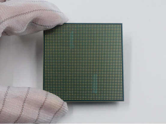
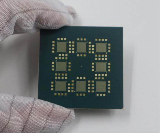
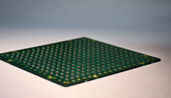
Package dimensions must always be selected based on the physical size of the silicon die. The die’s length, width, and thickness set the minimum internal cavity size the package must accommodate. If the die is large or contains many functional blocks, it typically requires a package with more internal space—such as a BGA (Ball Grid Array) or other substrate-based package. These formats support large dies and high I/O counts while maintaining mechanical stability.
In contrast, ultra-thin dies used in wearables, sensors, and compact mobile devices are well suited for WLP (Wafer-Level Package) and FOWLP (Fan-Out Wafer-Level Package). These packages minimize thickness and eliminate the need for a traditional leadframe or substrate, making them ideal for space-constrained designs. The key point is simple: the package must physically fit the die while supporting its electrical and thermal needs.
Miniaturization Trends in Modern Electronics
Modern electronics continue to push for smaller, thinner, and lighter products. This trend affects package selection because smaller packages help reduce overall system size and improve electrical performance. A compact package reduces the PCB area required, allowing more components to be placed in the same space or enabling the product to shrink in size.
Smaller packages also create shorter signal paths, which reduce parasitic capacitance and inductance. This leads to better RF performance, improved power efficiency, and higher signal integrity—critical advantages for smartphones, wearables, Wi-Fi modules, and high-frequency communication devices. As a result, miniaturized packages like QFN, WLP, and FOWLP have become standard choices in consumer electronics.
Key Considerations When Selecting Package Size
Selecting the right package size requires balancing several trade-offs. A thinner package can improve portability, but it may reduce thermal capacity or limit material options. A smaller footprint saves board space but may demand tighter PCB routing rules or higher-density interconnects. Designers must consider how package size affects thermal performance, footprint, and board area, especially in power-intensive or high-speed applications.
Package size also affects assembly yield and warpage risk. Larger or very thin packages may warp during reflow, leading to solder joint issues or misalignment. Smaller packages, while easier to cool and route, may require more precise placement and inspection. The best choice is the one that balances system requirements with manufacturability, ensuring stable performance throughout both production and field operation.
Pin Count Requirements — Matching I/O Needs
Ensuring Sufficient Electrical Connections
The number of pins or pads in a package must always be greater than or equal to the total number of electrical connections required by the chip. These connections include input pins, output pins, control interfaces, power pins, and ground pins. If the package lacks enough I/O capacity, the chip cannot function as intended, regardless of its internal capabilities.
Different package families are designed to support different I/O ranges.
Low I/O requirements are typically served by compact packages such as QFN or SOP, which offer a small footprint and simple routing.
Medium I/O requirements often fit well with QFP packages, which provide more pins along the perimeter while remaining cost-effective.
High I/O requirements—common in processors, FPGAs, and high-speed communication chips—usually require BGA, LGA, or flip-chip BGA packages. These formats provide hundreds or even thousands of connections in a dense grid, far beyond what perimeter-only packages can support.
The key principle is straightforward: the package must offer enough I/O bandwidth to match the chip’s functional and power delivery needs.
High-Density Interconnect (HDI) Implications
As pin count increases, the package naturally adopts a finer pitch, meaning the distance between pins or solder balls becomes smaller. Finer pitch packages demand more advanced PCB technologies, known collectively as HDI (High-Density Interconnect). HDI boards use methods such as via-in-pad, microvias, and buried vias to route signals between the closely spaced pads of modern IC packages.
Higher pin counts significantly affect PCB design. More pins require additional routing channels, which often increases the PCB layer count to maintain signal integrity and proper power distribution. As the number of layers grows, so does the PCB cost—sometimes substantially. Designers must also account for impedance control, escape routing strategy, and manufacturing tolerances when working with dense BGA or flip-chip layouts.
Because of these factors, selecting a high-pin-count package is not only a packaging decision but also a PCB technology and cost decision. Understanding the HDI implications early helps ensure that both the package and the board can support the chip’s performance targets without exceeding the project’s budget or manufacturing capability.
Reliability Requirements — Choosing Based on Application
Comparing Packaging Materials
Plastic Packages
Plastic packages are the most common choice for consumer and industrial electronics due to their low cost and widespread availability. These packages use epoxy molding compounds and are classified as non-hermetic, meaning they do not create a fully sealed barrier against moisture or gases. Because of this, plastic packages typically offer lower mechanical strength, limited moisture resistance, and reduced long-term stability compared to ceramic options.
Despite these limitations, plastic packaging remains ideal for everyday devices—such as home appliances, handheld electronics, and general industrial equipment—where cost efficiency and moderate reliability are sufficient. Their balance of performance, manufacturability, and price makes them the default option for high-volume applications.
Ceramic / Metal-Ceramic Packages
Ceramic and metal-ceramic packages are designed for high-reliability environments. They provide hermetic sealing, meaning the package forms a gas-tight enclosure that protects the die from moisture, contamination, and oxidation. These materials offer excellent thermal stability, high mechanical strength, and superior resistance to chemical and environmental stress.
Because of these advantages, ceramic and metal-ceramic packages are widely used in aerospace systems, satellites, medical implants, and high-reliability automotive components. These applications demand long operational lifetimes, stable performance in harsh conditions, and absolute protection from environmental factors.
When High-Reliability Packaging Is Needed
High-reliability packaging becomes essential when the IC must operate in extreme temperatures, under strong vibration or shock, or in high-radiation environments. For example, avionics control systems may face large temperature swings, while spacecraft electronics must tolerate radiation and vacuum exposure. In such cases, choosing ceramic or metal-ceramic packaging is not optional—it is a requirement for mission success.
Reliability verification often involves rigorous testing such as thermal cycling, humidity resistance, mechanical stress testing, and accelerated aging. These tests help confirm that the package will protect the die throughout the product’s entire lifecycle. The key principle is clear: when the environment is harsh or failure is unacceptable, high-reliability packaging is mandatory.
Thermal & Electrical Performance — Meeting Power and Speed Requirements
Heat Generation in IC Operation
Modern ICs generate increasing amounts of heat due to higher power densities from smaller transistor nodes and faster operating frequencies. As chips shrink and switch faster, the energy per unit area rises, creating thermal challenges. Without effective heat dissipation, ICs may experience throttling, where performance is intentionally reduced to prevent overheating. Prolonged exposure to high temperatures can also lead to electromigration, where metal interconnects degrade, or premature failure of the device. Understanding heat generation is critical to selecting a package that can manage the thermal load efficiently.
Thermal Simulation & Electrical Simulation
Before finalizing a package, engineers often use thermal and electrical simulations to validate design choices. Thermal simulations calculate the junction-to-ambient thermal resistance (RθJA) and predict temperature rise under expected operating conditions. Electrical simulations evaluate impedance, inductance, and capacitance of the package, which are essential for maintaining signal integrity in high-speed designs. These simulations ensure that material selections, die placement, and package geometry will meet performance and reliability requirements before manufacturing begins.
Enhancing Thermal Performance with Package Design
Material Choices
Selecting the right materials is a key factor in thermal management. Packages often use low-resistance materials and high-thermal-conductivity adhesives to improve heat transfer from the die to the package and PCB. High-conductivity molding compounds further enhance heat dissipation in encapsulated packages, helping to maintain safe operating temperatures under heavy workloads.
Structural Enhancements
Beyond materials, package structures can be optimized to improve thermal performance. Common techniques include exposed thermal pads (ePad), built-in heat spreaders, and metal blocks integrated into the package to channel heat away from the die. Examples of packages designed for enhanced thermal performance include:
HSPBGA (High-Spread Package BGA)
HSBGA (High-Speed BGA)
EDHS-QFP / DHS-QFP (Enhanced/Dual-Heat Spreader QFP)
QFN with thermal pad
E-Pad LQFP
These designs allow high-power ICs to operate reliably while maintaining compact form factors.
Electrical Integrity in High-Speed Packages
High-speed and high-frequency ICs, such as RF modules, 5G transceivers, and SerDes devices, require careful control of parasitic elements like inductance and capacitance. Packages with excessive parasitics can degrade signal quality and increase power loss. Flip-chip packages reduce parasitic effects by placing the die directly onto the substrate, minimizing wire lengths compared to traditional wire-bond designs. Selecting the right package ensures both thermal stability and electrical integrity, enabling high-speed ICs to meet stringent performance requirements.
Cost Considerations — Balancing Performance and Budget
Cost Drivers in Package Selection
The cost of an IC package depends on multiple factors. Package size is a major driver—larger packages require more material and complex handling, leading to higher costs. Material type also matters: packages built on substrates are generally more expensive than traditional leadframe packages because they provide better thermal and electrical performance but involve more intricate manufacturing. Similarly, layer count in substrate-based packages affects cost: multi-layer substrates increase PCB complexity and fabrication expenses compared to single-layer designs. Understanding these cost drivers helps engineers make informed decisions without compromising critical performance.
Aligning Cost with Product Positioning
Package selection should reflect the market positioning and end-use requirements of the product. For consumer electronics, cost efficiency is paramount, making plastic QFN or BGA packages ideal due to their low price and adequate performance. Automotive and industrial applications demand higher reliability, so mid-range packages that balance cost and robustness are preferred. In defense, aerospace, and space-grade electronics, reliability outweighs cost, requiring ceramic or metal-ceramic packages to withstand extreme conditions. Selecting the right package for the target market ensures the product is both competitive and dependable.
Avoiding Over-Engineering
Over-engineering occurs when designers choose a high-end package unnecessarily, adding cost without meaningful performance benefits. For instance, using a ceramic package for a low-power MCU intended for consumer applications is typically excessive. Instead, a standard plastic QFN would satisfy performance requirements at a fraction of the cost. Avoiding over-engineering helps maintain production efficiency, market competitiveness, and reasonable bill-of-materials (BOM) cost while still meeting reliability and performance targets.
The key principle is clear: package selection must strike a balance between performance, reliability, and cost, tailored to the product’s functional and market requirements.
Practical Decision-Making Flow for Package Selection
Step-by-Step Package Selection Framework
Selecting the right IC package involves a structured process to balance performance, reliability, manufacturability, and cost. A step-by-step framework can guide designers through this complex decision-making process:
1. Define I/O and Power Requirements
Identify the total number of electrical connections, including signal, power, and ground pins, as well as the expected power consumption. This ensures the package can handle the chip’s functional and energy needs.
2. Determine Assembly Method and PCB Constraints
Decide whether THT (Through-Hole) or SMT (Surface-Mount Technology) is appropriate, considering PCB density, manufacturing capabilities, and cost constraints. High-density boards often favor SMT packages like QFN or BGA.
3. Evaluate Size, Thickness, and Form Factor Limits
Assess the die dimensions, device thickness, and board space. Smaller, thinner packages reduce PCB area and improve signal integrity but may limit thermal performance or increase assembly complexity.
4. Assess Thermal and Electrical Performance Requirements
Perform initial calculations or simulations to verify that the package can dissipate heat efficiently and maintain signal integrity under the expected operating conditions. Packages with thermal pads, heat spreaders, or high-conductivity materials may be required for high-power or high-frequency devices.
5. Analyze Reliability Level and Industry Standards
Match the package material and design to the application environment. Use plastic packages for standard consumer electronics, and ceramic or metal-ceramic packages for high-reliability sectors like aerospace, automotive, or defense.
6. Estimate Cost and Match Product Market Segment
Align package choice with budget and market positioning. Consider substrate type, layer count, and size, ensuring the cost does not exceed what is justified by the product’s performance and target market.
7. Validate with Simulations & Prototype Testing
Conduct thermal, electrical, and mechanical simulations, followed by prototype assembly and testing, to confirm that the chosen package meets all performance, reliability, and manufacturability requirements.
Example Selection Scenarios
High-Power AI Chip → Flip-chip BGA with an exposed heat slug to maximize thermal dissipation and maintain signal integrity.
IoT Sensor → Ultra-small QFN or WLP to achieve compact form factor and low-cost production.
Automotive Controller → Ceramic or metal-ceramic package to ensure long-term reliability under temperature extremes and vibration stress.
This structured approach ensures that each package selection is systematic, justified, and optimized for the product’s electrical, thermal, mechanical, and economic requirements.
Conclusion — Packaging Choices Define Product Success
Selecting the right IC package is far more than a manufacturing decision—it is a strategic choice that directly shapes the success of the final product. The correct package minimizes the risk of failure, ensures stable electrical and thermal performance, supports reliable assembly, and optimizes overall cost. Conversely, mismatched packaging can introduce signal issues, thermal bottlenecks, or unnecessary expenses, potentially compromising both performance and market competitiveness.
At PCBMASTER, we understand that high-quality IC substrates are the backbone of reliable packaging solutions. Our advanced R&D and precision manufacturing capabilities—from ultra-fine line width of 25μm and microvia drilling to AS9100 aerospace-grade quality control—ensure that every substrate meets stringent electrical, thermal, and mechanical requirements. By combining premium materials, rigorous testing, and customer-focused service, PCBMASTER helps designers and manufacturers translate optimal package selection into real-world product success.
Whether the project demands high-speed AI processors, compact IoT sensors, or rugged automotive controllers, the right package and substrate pairing is key to unlocking performance, reliability, and efficiency in today’s competitive electronics market.
FAQs
How do I determine whether an IC should use THT or SMT packaging?
The choice between Through-Hole Technology (THT) and Surface-Mount Technology (SMT) depends on assembly method, PCB constraints, and application needs. THT is ideal for components requiring strong mechanical attachment, easy prototyping, or legacy systems, such as power modules and industrial hardware. SMT, on the other hand, supports smaller footprints, higher I/O density, and better high-frequency performance, making it the standard for modern consumer electronics, mobile devices, and high-speed applications.
What package types are best for high-power or high-heat IC applications?
High-power or high-heat ICs benefit from packages designed to enhance thermal performance. Options include flip-chip BGA, HSPBGA, HSBGA, EDHS-QFP, DHS-QFP, and QFN with thermal pads. These packages often feature exposed heat slugs, built-in heat spreaders, and high-conductivity materials to efficiently dissipate heat and maintain electrical integrity under high-power conditions.
How does pin count influence the choice of IC package?
The total I/O count determines which package can accommodate all necessary connections. Low I/O chips typically use QFN or SOP, medium I/O designs fit well with QFP, and high I/O devices—like processors or high-speed ICs—require BGA, LGA, or flip-chip BGA. Higher pin counts also demand fine-pitch HDI PCB designs with microvias and additional layers to route all signals effectively.
Why are ceramic packages preferred in aerospace electronics?
Ceramic and metal-ceramic packages are hermetically sealed, providing excellent resistance to moisture, temperature extremes, vibration, and radiation. These properties make them ideal for aerospace, and high-reliability automotive applications, where long-term performance and environmental resilience are critical.
How does package size impact PCB design and system performance?
Package size affects board space, signal paths, thermal performance, and assembly yield. Smaller, thinner packages save PCB area, allow shorter signal paths, and improve high-frequency performance. Larger packages may support higher pin counts or better heat dissipation but occupy more board area and can increase risk of warpage during assembly. Designers must balance size, thermal management, and routing requirements to optimize system performance.

