


Flexible PCB Material Selection: Tips for Engineers and Designers
In today’s fast-evolving electronics landscape, devices are becoming smaller, lighter, and more adaptable than ever before. Flexible PCBs play a crucial role in enabling this transformation, bending and folding to fit into designs that once seemed impossible. Choosing the right material isn’t just a technical decision—it can define the performance, durability, and success of the final product. From wearable gadgets to aerospace systems, understanding how materials behave under real-world conditions is key to unlocking innovation.
Introduction to Flexible PCB Materials
Definition and Overview of Flexible PCBs
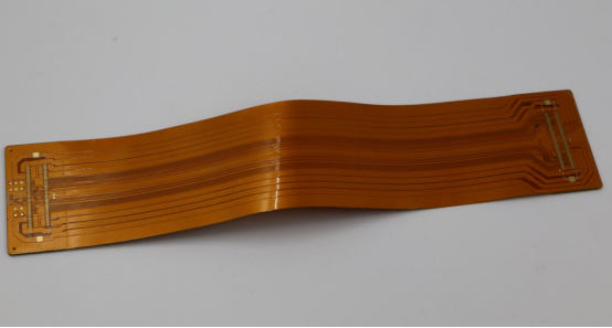
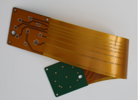
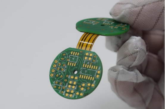
Flexible PCBs, or flex circuits, are printed circuit boards designed to bend, fold, or twist without breaking. Unlike traditional rigid PCBs, which are made from solid substrates like FR-4, flexible PCBs use thin, bendable materials such as polyimide or polyester films. This flexibility allows engineers to fit electronic circuits into unconventional shapes and compact spaces.
Flexible PCBs differ from rigid boards in several ways. They can absorb mechanical stress, conform to curved surfaces, and reduce the number of connectors needed in a device. For example, in a smartwatch, a flexible PCB can wrap around the battery and sensors, creating a slimmer profile than rigid boards would allow. In medical devices, flexible circuits enable wearable monitors that follow body contours, while in aerospace applications, they can withstand vibration and temperature variations in confined spaces.
Key takeaway: Flexible PCBs combine electrical functionality with mechanical adaptability, making them essential for compact, dynamic, or high-performance electronics.
Importance of Material Selection
Choosing the right material for a flexible PCB is critical because it directly affects the board’s performance, reliability, and manufacturability. Materials must handle mechanical stress without cracking, tolerate thermal cycles during operation or soldering, and support signal integrity in high-speed circuits. For instance, selecting a low-quality polyimide film might save cost upfront but could lead to delamination or failure in a wearable device over time.
Material selection also has long-term cost implications. High-performance substrates may cost more per unit but reduce the risk of board failure, lower maintenance needs, and increase product lifespan. Conversely, cheaper materials may limit design options or require additional reinforcement layers, increasing assembly complexity. Step-by-step, engineers should evaluate mechanical flexibility, thermal stability, chemical resistance, and electrical properties before finalizing a material choice.
In essence, the right material ensures the flexible PCB can meet design goals while balancing cost, manufacturability, and durability, making it a foundational decision in any electronics project.
Types of Flexible PCB Materials
Base Substrates
The base substrate is the core material of a flexible PCB that determines its mechanical strength, thermal performance, and overall durability. Two common types are Polyimide (PI) and Polyester (PET).
Polyimide (PI): Polyimide is a high-performance substrate known for its excellent temperature tolerance and flexibility. It can withstand continuous operating temperatures up to 260°C and is resistant to chemical corrosion. This makes PI ideal for high-reliability applications like aerospace electronics, medical devices, and high-frequency circuits.
Polyester (PET): Polyester is a cost-effective alternative, offering flexibility at a lower price point. However, PET has lower thermal resistance, typically up to 150°C, making it better suited for consumer electronics, LED lighting, and short-term wearable devices.
Comparison Table: Base Substrate Properties
Property | Polyimide (PI) | Polyester (PET) |
|---|---|---|
Flexibility | High | Moderate |
Maximum Operating Temp | 260°C | 150°C |
Mechanical Strength | Strong | Moderate |
| Dielectric Constant | Low (good for signal integrity) | Moderate |
Key takeaway: Selecting the right substrate depends on temperature requirements, flexibility needs, and cost constraints.
Copper Foil Options
Copper foil forms the conductive layer of a flexible PCB and directly affects its flexibility, electrical performance, and reliability. There are two main types: Rolled Annealed (RA) and Electrodeposited (ED) copper.
Rolled Annealed (RA) Copper: RA copper is mechanically rolled and annealed, giving it high ductility. It bends easily without cracking, making it ideal for flex circuits that undergo repeated mechanical stress.
Electrodeposited (ED) Copper: ED copper is deposited through an electroplating process. It has higher strength but lower flexibility, which is suitable for applications where mechanical stress is minimal.
Key impact: RA copper improves bend reliability and reduces the risk of trace cracking, while ED copper may be preferred for high-current applications where rigidity is less of a concern.
Adhesives and Laminates
Flexible PCBs can be constructed using adhesive-based or adhesiveless laminates, each with advantages depending on application requirements.
Adhesive-Based Flexible PCBs: These PCBs use a thin adhesive layer to bond copper foil to the substrate. They are easier to manufacture and cost-effective, but repeated thermal cycling can cause delamination or reduced flexibility over time.
Adhesiveless Flexible PCBs: Adhesiveless designs directly bond copper to the substrate without an intermediate adhesive. They offer superior thermal resistance, better flexibility, and enhanced reliability under mechanical stress.
Comparison Summary:
Adhesive-based: simpler, cheaper, slightly lower durability
Adhesiveless: higher performance, more resilient to heat and repeated bending
Key takeaway: Choosing the right laminate or adhesive type ensures the flexible PCB can handle expected mechanical and thermal conditions without compromising reliability.
Key Material Properties to Consider
Mechanical Properties
Mechanical properties are critical for flexible PCBs because they determine how well the board can bend, twist, or stretch without damage. Key factors include flexibility, bend radius, and tensile strength. Flexibility measures how easily the material can deform, while tensile strength indicates the material’s resistance to being pulled or stretched.
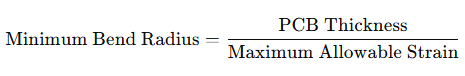
Step-by-step: Calculating Minimum Bend Radius
1. Identify the thickness of the PCB, including the substrate and copper layers.
2. Determine the material’s maximum strain tolerance (often provided by the manufacturer).
3. Apply the formula:
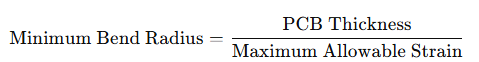
4. Verify the radius meets your design’s mechanical requirements.
Example: A 0.2 mm thick polyimide PCB with a maximum strain of 1% would have a minimum bend radius of 20 mm. Designing below this radius increases the risk of cracks or delamination.
Key takeaway: Mechanical properties guide how the PCB can physically fit into compact or dynamic designs without failure.
Thermal and Electrical Properties
Thermal and electrical characteristics influence performance, signal integrity, and long-term reliability. Two important thermal metrics are Tg (glass transition temperature) and Td (decomposition temperature):
Tg is the temperature at which the substrate softens. Exceeding Tg can lead to dimensional changes or warping.
Td is the temperature at which the material chemically decomposes. Operation near Td can cause permanent failure.
Electrical properties, including dielectric constant (Dk) and dissipation factor (Df), affect signal speed, attenuation, and crosstalk. Low Dk materials reduce signal delay, while low Df minimizes energy loss in high-frequency circuits.
Example: For a flexible PCB in a 5G antenna module, selecting a substrate with low Dk and Df ensures stable signal propagation and minimal interference.
Key takeaway: Thermal and electrical properties must match the operational environment and performance requirements of the device.
Chemical and Environmental Resistance
Flexible PCBs are often exposed to harsh environments, making chemical and environmental resistance a key consideration. Important factors include resistance to moisture, solvents, and UV exposure.
Moisture can cause swelling or delamination, affecting reliability in humid conditions.
Solvents used during cleaning or assembly can degrade adhesives or copper adhesion.
UV exposure may degrade some polymer substrates over time.
Examples by application:
Aerospace electronics require high resistance to temperature extremes, humidity, and chemical exposure due to altitude and pressure variations.
Consumer electronics, like smartwatches, face moderate moisture and UV exposure but require compact, flexible designs.
Key takeaway: Choosing materials with the right chemical and environmental resistance ensures the PCB performs reliably in its intended operating conditions.
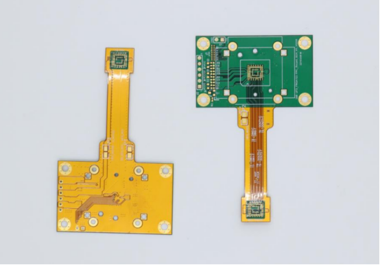
Design and Application Considerations
Layer Count and Material Stack-Up
The layer count and material stack-up of a flexible PCB directly affect its flexibility, signal integrity, and overall reliability.
Single-layer flexible PCBs consist of a single conductive layer on a substrate. They are highly flexible, easy to manufacture, and ideal for simple circuits or low-density designs.
Multi-layer flexible PCBs have multiple conductive layers separated by insulating layers. While they allow higher circuit density and complex routing, they are less flexible and require careful stack-up planning to maintain bendability.
Impact on signal integrity: Multi-layer stack-ups with proper ground and power planes reduce electromagnetic interference (EMI) and improve high-frequency performance. Improper stack-up can cause signal reflections, crosstalk, or impedance mismatches.
Key takeaway: Choosing the right layer count balances flexibility, circuit complexity, and electrical performance.
Trace Width, Spacing, and Copper Thickness
Trace geometry and copper thickness are critical to electrical performance and mechanical reliability.
Recommended trace widths: Flexible PCB traces are often narrower than rigid boards to maintain bendability. Standard widths range from 3–10 mils, depending on current requirements.
Copper thickness comparison:
- Thin copper (0.5 oz/ft²) is more flexible, suitable for repeated bending, but carries lower current.
- Thick copper (2 oz/ft² or higher) can handle high-current applications but reduces flexibility and increases minimum bend radius.
Example: In a foldable device, using 1 oz copper traces allows the board to bend repeatedly without cracking, while still supporting signal routing for most low-power circuits.
Key takeaway: Proper trace width, spacing, and copper thickness ensure current handling, flexibility, and long-term reliability.
Mechanical Stress and Reliability Testing
Flexible PCBs must withstand repeated bending, twisting, and thermal cycles. Mechanical stress and reliability testing verifies that the design can survive real-world conditions.
Step-by-step testing procedures:
1. Fold and flex testing: Repeatedly bend the PCB along critical areas to check for cracks or delamination.
2. Thermal cycling: Expose the PCB to alternating high and low temperatures to simulate operational and soldering conditions.
3. Electrical testing: Measure continuity and resistance before and after mechanical and thermal tests to identify potential failures.
Common failure modes and improvements:
Cracked traces → Use RA copper or increase bend radius.
Delaminated layers → Consider adhesiveless laminates or adjust stack-up.
Warping or curling → Optimize material selection and thickness distribution.
Key takeaway: Reliability testing identifies weak points and guides design improvements to ensure flexible PCBs perform under mechanical and thermal stress.
Cost vs. Performance Trade-Offs
Material Cost Comparison
Material choice significantly influences the overall cost of flexible PCBs, especially for large-scale production. Common substrates include polyimide (PI), polyester (PET), and specialty high-temperature films.
Polyimide (PI): Offers high thermal stability, excellent flexibility, and chemical resistance. PI is more expensive than PET but ensures long-term reliability in demanding applications.
Polyester (PET): Cost-effective and suitable for consumer electronics or low-stress applications. Lower thermal tolerance limits its use in high-temperature or high-frequency devices.
Specialty high-temp films: Advanced substrates such as liquid crystal polymer (LCP) provide extreme thermal stability and low dielectric loss, ideal for RF and aerospace applications, but at a premium cost.
Impact on production scale and ROI: Higher-cost substrates may increase unit cost but reduce failure rates, warranty claims, and redesigns, improving long-term ROI. Conversely, low-cost substrates may reduce upfront expenses but can result in higher maintenance costs and shorter product lifespan.
Key takeaway: Balancing material cost with application requirements is essential for optimizing production efficiency and ROI.
Balancing Performance Requirements
Performance requirements often dictate material selection. Flexible PCBs must meet demands for high-frequency signals, thermal limits, and mechanical flexibility simultaneously.
Step-by-step performance evaluation:
1. Identify operating environment (temperature, humidity, chemical exposure).
2. Determine electrical requirements (signal frequency, impedance, and loss).
3. Assess mechanical demands (bending, twisting, vibration).
4. Select materials that satisfy all criteria while keeping costs manageable.
Example: For a wearable device:
High-end polyimide can handle repeated bending and moderate heat, ensuring durability but at higher cost.
Budget PET may be sufficient for devices with minimal thermal stress, lowering manufacturing cost but with shorter lifespan.
Key takeaway: Engineers must weigh performance needs against material costs to achieve an optimal balance between reliability, functionality, and affordability.
Supplier and Manufacturing Considerations
Material Availability and Standardization
Flexible PCB materials must meet recognized industry standards to ensure quality and compatibility. Common certifications include IPC-2223, which defines flexible PCB design and fabrication guidelines, and UL 94V-0, which certifies flame retardancy. Manufacturers often offer standardized substrate grades from leading brands such as DuPont, Panasonic, SYTECH, and Taiwan Union, ensuring predictable electrical, thermal, and mechanical performance.
Key takeaway: Using standardized, certified materials simplifies manufacturing, improves reliability, and ensures compliance with industry regulations.
Manufacturing Constraints
Design choices such as minimum bend radius, layer count, and plating options directly affect manufacturability. Flexible PCBs with very thin substrates or multiple layers may require special handling to prevent delamination or trace cracking. Material selection also impacts lead time and production yield: high-performance substrates or rare materials can extend production timelines, while common grades are easier to source and produce efficiently.
Example: Choosing polyimide over PET may increase cost slightly, but it allows tighter bend radii and higher thermal tolerance, reducing failure rates during assembly.
Key takeaway: Understanding material-driven manufacturing constraints helps engineers optimize design for reliability, cost, and on-time delivery.
Quality Assurance and Testing
Reliable flexible PCB production requires rigorous quality assurance (QA) and testing at multiple stages. Typical QA steps include:
1. Electrical testing: Continuity, insulation resistance, and impedance verification.
2. Thermal cycling: Simulating operating temperature extremes to detect delamination or warping.
3. Dimensional checks: Verifying board thickness, hole sizes, and layer alignment.
4. Mechanical stress testing: Fold, bend, and flex tests to ensure durability under repeated use.
Examples of common checkpoints:
Minimum hole diameter verification (e.g., ≥0.05 mm for laser-drilled microvias)
Trace width and spacing compliance (e.g., 1.8 mil minimum for fine-pitch circuits)
Adhesion testing for laminates and coverlays
Key takeaway: Comprehensive QA ensures that flexible PCBs meet electrical, thermal, and mechanical specifications before shipment.
PCBMASTER Capabilities
PCBMASTER specializes in high-performance flexible and rigid-flex PCBs, offering fast delivery and advanced manufacturing capabilities:
Fast standard delivery: 7-day turnaround for 6–20 layer conventional rigid-flex boards.
HDI and multi-stage rigid-flex: Supports first-to-any-order HDI rigid-flex PCBs using high-quality materials from DuPont, Panasonic, and New High.
Ultra-thin flex boards: Minimum soft layer thickness as low as 0.8 mm, enabling compact, high-density designs.
Advantages of PCBMASTER FPCs:
Ultra flexibility and bend resistance, surviving over 100 million folding cycles
Ultra-thin and lightweight construction for compact devices
High-precision manufacturing with stringent QA and ISO-certified processes
Expert technical support to optimize design and reduce costs
Key takeaway: Partnering with a manufacturer like PCBMASTER ensures rapid production, reliable materials, and adherence to international quality standards, enabling engineers to focus on innovative designs rather than supply chain constraints.
Emerging Trends in Flexible PCB Materials
Advanced High-Flex Materials
Recent developments in flexible PCB technology have introduced ultra-thin copper foils and adhesive-free laminates, which offer exceptional flexibility and reliability. These materials can bend repeatedly without cracking or delaminating, making them ideal for foldable devices, wearable electronics, and high-density circuits.
Potential benefits:
Reduced minimum bend radius enables more compact designs.
Lower overall board thickness supports lightweight, ultra-thin electronics.
Adhesive-free laminates improve thermal cycling tolerance and long-term durability.
Example: Foldable smartphones and high-density medical sensors benefit from ultra-thin, high-flex laminates that maintain electrical integrity even after millions of bending cycles.
Key takeaway: High-flex materials allow designers to create complex, compact, and mechanically robust flexible PCBs.
Eco-Friendly and Recyclable Materials
Sustainability is becoming a priority in PCB manufacturing. Biodegradable substrates, lead-free copper, and low-VOC laminates reduce environmental impact while meeting regulatory and industry standards.
Advantages:
Biodegradable substrates minimize landfill waste for disposable electronics.
Lead-free copper ensures compliance with RoHS and other environmental regulations.
Low-VOC laminates reduce harmful emissions during production.
Example: Consumer electronics companies can use eco-friendly flexible PCBs in wearable devices to combine high performance with environmental responsibility.
Key takeaway: Eco-friendly materials support sustainable electronics without compromising mechanical or electrical performance.
Material Innovations for High-Frequency Applications
Flexible PCBs are increasingly required to support high-frequency and RF applications, including 5G devices and automotive radar systems. Low-loss substrates such as liquid crystal polymer (LCP) or advanced polyimide variants offer superior dielectric properties compared with traditional polyimide materials.
Comparison with traditional polyimide:
Low-loss substrates: Lower dielectric constant (Dk) and dissipation factor (Df), reducing signal attenuation at high frequencies.
Traditional polyimide: Adequate for moderate-frequency circuits but higher Dk/Df can limit performance in RF or mmWave applications.
Example: A 5G mmWave radar FPC using low-loss LCP substrate achieves lower insertion loss and better phase stability than a standard polyimide-based board.
Key takeaway: Innovative materials for high-frequency flexible PCBs enable reliable signal transmission in next-generation communication and radar systems.
Conclusion
Selecting the right materials is the foundation of reliable and high-performance flexible PCBs. Engineers should consider mechanical, thermal, and electrical requirements, compare substrates and copper types, and balance cost versus performance to ensure long-term durability and signal integrity. Early material decisions simplify design and manufacturing, reduce revisions, and improve production yield. Partnering with a trusted manufacturer like PCBMASTER provides access to high-quality flexible and rigid-flex PCBs, rapid prototyping, and expert support, helping bring complex designs to market efficiently and reliably.
FAQs
What is the most common substrate material for flexible PCBs?
The most common substrate material is polyimide (PI). It offers excellent flexibility, high thermal stability (up to around 260°C), and good chemical resistance, making it suitable for wearable electronics, medical devices, aerospace applications, and high-density flexible circuits. Polyester (PET) is also used for cost-sensitive or lower-temperature applications but provides lower thermal performance.
How do I calculate the minimum bend radius for a flexible PCB?
The minimum bend radius depends on the PCB thickness and the material’s maximum allowable strain. A simple formula is:
For example, a 0.2 mm thick polyimide PCB with a 1% maximum strain would have a minimum bend radius of 20 mm. Staying above this radius prevents trace cracking and delamination.
What are the main differences between RA and ED copper in flexible PCBs?
Rolled Annealed (RA) copper: Highly ductile and flexible, ideal for circuits that undergo repeated bending or flexing. Less prone to cracking under mechanical stress.
Electrodeposited (ED) copper: Stronger but less flexible, better suited for high-current applications with minimal bending.
Key takeaway: RA copper improves mechanical reliability, while ED copper can handle higher current loads but reduces flexibility.
Can flexible PCBs be used in high-temperature environments?
Yes, if the right substrate is chosen. Polyimide-based flexible PCBs can withstand continuous operating temperatures up to about 260°C, making them suitable for aerospace, automotive, and industrial applications. Lower-cost substrates like PET are limited to around 150°C and are not recommended for high-temperature conditions.
How does material choice affect signal integrity in flexible circuits?
Material properties such as dielectric constant (Dk) and dissipation factor (Df) influence signal speed, loss, and crosstalk. Low-loss substrates like advanced polyimide or LCP maintain high-frequency performance, reduce signal attenuation, and improve phase stability, while traditional materials with higher Dk/Df can degrade signal quality in high-speed or RF circuits.

