Double-Sided Aluminum and Copper PCBs: Key Features and Applications
As electronic devices grow smaller and more powerful, efficient heat management becomes increasingly crucial. Traditional circuit board materials often fall short when it comes to handling the intense thermal demands of modern applications. Double and multi-layer metal substrates offer a powerful solution, combining the strength of metal with superior thermal conductivity. These advanced substrates are transforming industries, from automotive power modules to high-end LED systems, enabling the design of more compact, high-performance electronics without compromising on heat dissipation.
What are Double/Multi-Layer Metal Substrates?
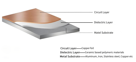
Metal-based circuit boards (often referred to as aluminum substrates or copper substrates, depending on the author’s preference) are copper-clad boards made with metal as the base material. These boards are thermally conductive composite materials widely used in electronic devices for heat dissipation. A single-layer metal substrate typically consists of three layers: the circuit layer (copper foil), a dielectric layer (low thermal resistance polymer), and the metal substrate (aluminum or copper). These substrates are known for their high thermal conductivity, electrical insulation, and mechanical workability.
Single-layer metal substrates are commonly used in Surface-Mount Technology (SMT) to connect components. The thermally conductive insulating layer, which utilizes ceramic-filled polymer technology, supports copper foil thicknesses from 35μm to 350μm (1oz-10oz) to conduct high currents, while the metal base layer provides structural support and heat dissipation. These substrates offer better heat dissipation than traditional FR-4 PCBs, lowering device temperatures and extending their lifespan. They are widely used in circuit designs with high thermal management requirements and can replace most ceramic substrates to reduce costs, making them a critical material for electronic products that demand excellent heat management.
However, traditional single-sided designs only allow for component mounting on one side and support single-layer circuitry. This limitation has led to the development of double-sided metal substrates, which enable both sides of the board to be used for circuit layout and component mounting. Additionally, through-hole assembly (THT) can be employed for the assembly of through-hole components, allowing for more complex circuit connections and double-layer wiring.
Differences in Manufacturing Processes Between Single-Sided and Double-Sided Metal PCBs
Lamination: Double-layer (or multi-layer) metal substrates, compared to single-sided PCBs, require a more complex lamination process involving the mixing of multiple materials. This increases manufacturing costs and places higher demands on production technology.
Drilling: When manufacturing double-sided metal substrates, drilling is done twice or more to ensure the proper placement of vias.
Resin Filling: Since metal is conductive, copper cannot be directly plated inside the drilled holes of the metal base. After drilling, a resin layer is applied to the holes to form an insulating layer. Afterward, a second drilling process ensures hole concentricity, followed by electroplating and other post-processing steps.
Process Comparison: The production process of a single-sided metal substrate involves the preparation of the metal base, the addition of a thermally conductive insulating layer, and copper foil coverage. This is followed by high-temperature compression molding to finalize the aluminum substrate. In contrast, the production of double-sided metal substrates is more complex. After machining the metal base, it undergoes pre-treatment and the insulation filling process for the vias. Then, thermally conductive insulating layers are applied to both sides, and copper foil is added. After high-temperature compression, additional processes like pattern transfer and re-machining are required to finalize the double-sided substrate.
Comparison Table: Differences in Manufacturing Processes Between Single-Sided and Double-Sided Metal Substrates
| Process Step | Single-Sided Metal Substrate | Double-Sided Metal Substrate |
| Lamination | Simple lamination process with one layer of copper and insulation. | More complex, involving multiple layers and materials for both sides. |
| Drilling | Single-side drilling for component placement. | Requires double drilling or more for vias on both sides. |
| Resin Filling | Not required. | Resin filling of vias for insulation, followed by secondary drilling. |
| Manufacturing Process | Metal base preparation, thermal insulation, copper foil coverage, and compression molding. | Metal base machining, pre-treatment, insulation filling, double-side lamination, and re-machining. |
| Complexity | Relatively simpler and faster. | More complex, involving additional steps for both sides and vias. |
| Cost | Lower cost due to simpler manufacturing. | Higher cost due to increased complexity and additional materials. |
Core Structure and Performance Characteristics of Double/Multi-Layer Metal Substrates?
The double-sided metal substrate typically comes in two main structures: one is the double-sided core metal substrate, and the other is the double/multi-layer composite metal substrate (a combination of double/multi-layer FR4 + high thermal conductivity insulating layer + metal base). Below are the key characteristics of these two structures:
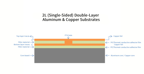
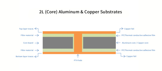
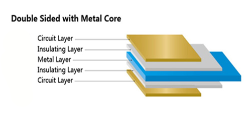
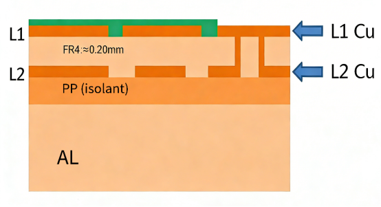
1. Double-Sided Core Metal Substrate: This structure is similar to a standard double-sided PCB, where both the top and bottom layers are used for circuit layout, while the core is made of metal. A double-sided core aluminum substrate is an important type of metal-based PCB. It features a five-layer symmetrical construction: the circuit layers (outer layers) + high thermal conductivity insulating material + metal core layer (support/heat dissipation core) + high thermal conductivity insulating material + circuit layers (outer layers). Electrical interconnection between the top and bottom circuits is achieved through metallized vias.
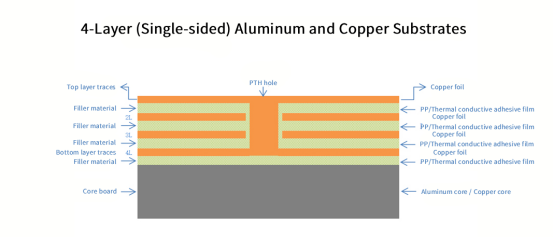
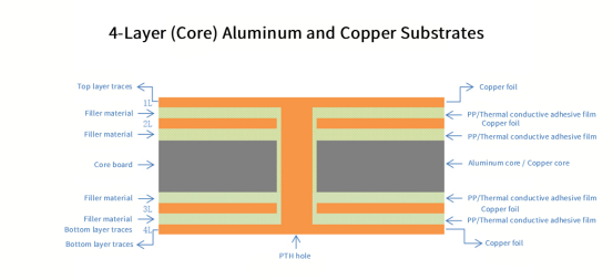
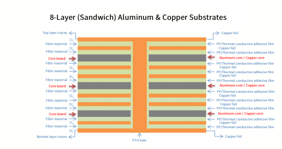
2. Double (Multi-Layer) Composite Metal Substrate: This structure typically consists of two (or more) layers of circuitry, a composite insulating layer, and a metal core layer. Electrical interconnection between the top and bottom circuits is achieved through metallized vias. The core features of this design are its excellent heat dissipation (the metal core quickly conducts heat away, while the composite insulating layer ensures efficient thermal conduction and electrical insulation), the capability for high-density dual (or multi)-layer wiring (suitable for complex circuit designs), and the composite materials that enhance mechanical strength and resistance to interference (such as electromagnetic shielding and moisture/thermal shock resistance). Typically, the structure combines double (or multi)-layer FR-4 with the metal core through lamination, but after lamination, only the top layer is used for component mounting. This design also allows for Through-Hole Technology (THT) assembly.

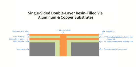
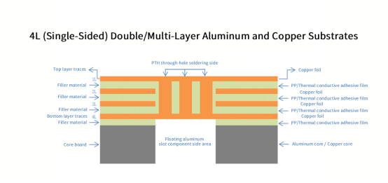
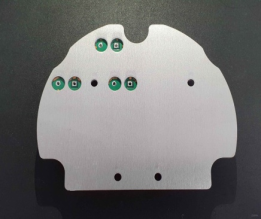 The image above shows a single-sided, double-layer aluminum substrate capable of supporting Through-Hole Technology (THT) assembly
Why Design Double-Sided Metal Substrates (Double-Sided Aluminum or Copper Substrates)?
At first glance, designing double-sided metal substrates might seem counterintuitive, as metal substrates are primarily intended for heat dissipation from the backside. However, they were specifically developed to address unique challenges in highly integrated, high thermal density, and high reliability applications. Rather than replacing traditional single-sided metal substrates, they extend and complement their functionality.
Below are the core reasons and applications for designing double-sided aluminum substrates:
1. Core Driver: Achieving Higher Density and More Complex Circuit Layouts
Limitations of Single-Sided Metal Substrates: With single-sided metal substrates, circuitry and components can only be arranged on one side (top layer), limiting the available surface area for complex designs. When circuits become more intricate and component count increases, a larger board is needed, which not only drives up costs but could also lead to space constraints.
Advantages of Double-Sided Metal Substrates: Much like conventional double-sided FR-4 PCBs, double-sided metal substrates allow for circuit and component placement on both the top and bottom layers. This brings revolutionary benefits:
Doubling the Wiring Space: Without increasing the board size, it can accommodate more complex circuitry.
Enabling Cross-Wiring: By using metallized vias to connect the two layers, double-sided designs eliminate the need for crossing lines, significantly enhancing the freedom of circuit layout.
Space Saving: By moving certain components to the bottom layer, a more compact and efficient package can be achieved.
2. Key Premise and Core Value: Maintaining Exceptional Heat Dissipation While Achieving Double-Sided Wiring
This is the essence of double-sided metal substrates. The goal is not just to enable double-sided wiring, but to ensure that heat generated on both sides can be efficiently dissipated.
The Problem with Traditional Solutions: In a traditional dual-sided FR-4 PCB design, when placed on a heatsink, only the components on the side in direct contact with the heatsink will dissipate heat effectively. The components on the backside have to rely on heat traveling through the entire PCB and the surrounding air, leading to poor thermal performance.
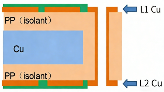
The Double-Sided Metal Substrate Solution: The typical structure of a double-sided metal substrate is a symmetrical "copper trace - insulating layer - aluminum core - insulating layer - copper trace" sandwich. The metal core serves as a shared heat dissipation channel:
Top-side Heat-Generating Components: Heat from the top components is transferred through the top insulating layer to the metal core.
Bottom-side Heat-Generating Components: Heat from the bottom components is transferred through the bottom insulating layer to the same metal core.
All the heat converges into the metal core, which then dissipates it uniformly. This results in the effective "temperature equalization" and superior heat dissipation for double-sided heat-generating components.
3. Main Application Scenarios (Where Are They Used?)
Due to the above features, double-sided metal substrates are widely used in high-end applications, including:
Automotive Electronics (Especially Electric/Hybrid Vehicles):
On-Board Chargers, DC-DC Converters: These applications have extremely high power density, featuring many MOSFETs, transformers, and other heat-generating components. Double-sided layouts are necessary to reduce the module size while ensuring effective cooling for all power components.
Motor Controllers/Inverters: These also face challenges with high power density and heat dissipation.
High-End, High-Power LED Products:
Automotive Headlights, High-Lumen Stage Lights, Plant Growth Lights: To achieve ultra-high brightness, large numbers of high-power LEDs are densely packed. A double-sided design allows for more LEDs or driver ICs to be placed and ensures efficient heat dissipation through the metal core, preventing light degradation.
High-Density Power Modules:
Server Power Supplies, Communication Base Station Power Supplies: These require small module sizes, high power, and high reliability. Double-sided aluminum substrates allow the separation of control and power circuits on different sides, optimizing layout and providing unified heat dissipation.
RF Power Amplifiers:
Certain high-power RF devices require excellent grounding and heat dissipation. A double-sided design provides a superior RF ground plane (on the bottom layer), while heat-generating components can be mounted on the top layer for heat dissipation through the metal substrate.
4. Design Challenges and Process Key Points
The manufacturing process for double-sided metal substrates is much more complex than that for single-sided versions, and it comes with higher costs. The main challenges include:
Metallized Vias: These are crucial for electrical connections. A hole must be drilled through the metal substrate, then insulated (by filling or covering the hole wall with high insulation material), followed by electroplating copper to make the via conductive. This process is both a technical challenge and a significant cost driver.
Symmetry Control: To ensure uniform heat dissipation on both sides and to prevent warping, the copper thickness and insulating layer thickness on both sides must be highly symmetrical.
High Precision Alignment: Double-sided circuitry requires precise alignment through vias to ensure proper connection and functionality.
Conclusion
The development of double-sided and multi-layer metal substrates has proven to be a game changer in tackling the challenges of heat dissipation and circuit density in modern electronics. These advanced substrates enable more efficient designs and provide superior performance in applications that demand both compactness and reliability, such as automotive electronics, high-power LEDs, and RF amplifiers. While the manufacturing process can be complex and costlier, the enhanced capabilities they offer in high-performance systems are invaluable.
For those navigating the intricacies of metal-based PCBs and seeking tailored, high-quality solutions, it's crucial to partner with experts who understand both the technical and application-specific challenges. At PCBMASTER, our experience and innovative approach ensure that we deliver the right solutions for your unique needs, helping you achieve optimal performance, reliability, and thermal management in your projects. Let’s collaborate to bring your designs to life with precision and efficiency.
FAQs
1. What are the main advantages of using metal substrates in PCBs?
Metal substrates, especially aluminum and copper, offer excellent heat dissipation properties compared to traditional FR-4 PCBs. This makes them ideal for applications where managing heat is crucial, such as power electronics, LED lighting, and automotive systems. Additionally, metal substrates provide improved mechanical strength and durability, making them more reliable in harsh environments.
2. How does a double-sided metal substrate improve circuit design flexibility?
A double-sided metal substrate allows for circuit components to be placed on both the top and bottom layers, effectively doubling the available surface area for wiring and component placement. This flexibility enables more complex and compact designs, reduces the need for larger boards, and provides better routing options, particularly for high-density applications.
3. Why are metallized vias important in double-sided metal substrates?
Metallized vias are crucial for connecting the top and bottom circuit layers in a double-sided metal substrate. They provide the electrical path for signals and power between the layers, and their quality and precision are essential for maintaining the integrity of the electrical connection, especially in high-density or high-power applications.
4. What challenges do manufacturers face when producing double-sided metal substrates?
Producing double-sided metal substrates presents challenges such as ensuring the symmetry of the copper and insulating layers on both sides, which is necessary for even heat dissipation and preventing warping. The metallization of vias is another challenge, requiring careful insulation and electroplating. Additionally, the manufacturing process is more complex, leading to higher production costs compared to single-sided PCBs.
5. In what types of products are double-sided metal substrates commonly used?
Double-sided metal substrates are commonly used in products that require high power density and efficient heat management, such as automotive electronics (e.g., on-board chargers and motor controllers), high-power LED lighting (e.g., automotive headlights and stage lighting), high-density power modules (e.g., server power supplies), and RF power amplifiers. Their ability to support complex circuits while managing heat makes them ideal for these demanding applications.
Author Bio
Hi, I'm Carol, the Overseas Marketing Manager at PCBMASTER, where I focus on expanding international markets and researching PCB and PCBA solutions. Since 2020, I've been deeply involved in helping our company collaborate with global clients, addressing their technical and production needs in the PCB and PCBA sectors. Over these years, I've gained extensive experience and developed a deeper understanding of industry trends, challenges, and technological innovations.
Outside of work, I'm passionate about writing and enjoy sharing industry insights, market developments, and practical tips through my blog. I hope my posts can help you better understand the PCB and PCBA industries and maybe even offer some valuable takeaways. Of course, if you have any thoughts or questions, feel free to leave a comment below—I'd love to hear from you and discuss further!