Key Design, Layout and Cutting Considerations for Double-Sided Metal PCBs
Double-sided metal PCBs are prized for their exceptional thermal conductivity, mechanical strength, and compact design, making them a perfect fit for high-power applications such as LED lighting, power supplies, and automotive electronics. However, achieving these benefits requires meticulous attention to detail in every stage of their design and manufacturing process. The design and layout are particularly crucial, as even small design flaws can affect both performance and longevity. Additionally, the cutting and shaping of these PCBs demand precision to prevent material deformation and ensure the integrity of each layer.
Key Considerations for the Design and Layout of Double-Sided Metal PCBs
Designing double-sided metal PCBs is a complex, multidisciplinary process that requires balancing electrical performance, thermal management, mechanical structure, and manufacturing processes. Compared to standard PCBs or single-sided aluminum baseboards, double-sided metal PCBs present significantly more design challenges and constraints. Below are the key considerations to keep in mind during the design process:
1. Electrical Design Considerations
Insulation Voltage and Creepage Distance:
This is the top priority for safety design. The total thickness of the insulation layers (both sides) and their material must be chosen based on the highest operating voltage, including transient surges, to ensure adequate dielectric strength.
Spacing:
Due to the conductive metal core between the layers, electrical isolation between the top and bottom layers depends entirely on the quality of the vias and the insulation layer. Specific attention should be given to:
Same Network Vias: Vias connecting the same network are typically safer since the metal core between them is at the same potential.
Different Network Vias/Tracks: Vias that belong to different potential networks are separated only by the insulating material in the holes. Sufficient spacing between these vias is necessary to prevent breakdowns, often requiring stricter hole-spacing rules than standard PCBs.
Via Design and Processing:
Vias in double-sided metal PCBs are unique and critical to the process. Vias serve as electrical conductors, insulators, and thermal pathways all at once. Common via types include:
Insulated Vias: These are the most common. After drilling, the holes are filled with a high-insulation, high-thermal-conductivity resin (such as epoxy resin with ceramic powder), and then plated to create electrical connections. The advantage is high mechanical strength, reliable insulation, and heat dissipation.
Via Wall Insulation (Electroplated Vias): This process involves depositing an insulating material on the via wall before electroplating copper for electrical conduction. This is a more complex and costly process.
Design Rules:
Via Diameter and Annular Ring: Communicate with manufacturers about their processing capabilities, as via filling can limit minimum hole diameters (usually >0.3mm). Larger pads and annular rings are required for reliable connections.
Vias Under Heat Sources: Vias can be strategically arranged below heat-generating components (such as ICs) to act as "thermal vias," helping to transfer heat more quickly from the top layer to the metal base. These vias are typically connected to ground or heat sink pads.
Grounding and Shielding:
The metal core of the PCB often serves as the ground plane. Connecting the core to the system’s ground potential provides a large, stable, low-impedance reference and acts as an electromagnetic shield. Multiple grounding vias should be used to create a strong electrical connection between the top and bottom layers, significantly improving EMI/EMC performance.
2. Thermal Design Considerations
Thermal Symmetry:
Both sides of the board are likely to have heat-generating components, so thermal simulation is necessary to analyze the temperature distribution when both sides are active. Balancing thermal load is critical—if one side has high-power components (like MOSFETs) and the other side has low-power control chips, the heat will predominantly be extracted from the high-power side. It might be necessary to add thermal connections on the low-power side (such as thermal pads contacting the outer casing) or adjust the layout to balance the heat load.
Insulation Layer Thermal Resistance:
While achieving double-sided routing, heat must travel through the insulation layer before reaching the aluminum core. Therefore, selecting insulation materials with high thermal conductivity (e.g., >2.0 W/mK) is crucial. The insulation thickness must be carefully balanced: thinner insulation reduces thermal resistance but weakens voltage resistance, so the optimal balance between thermal and voltage performance must be found.
External Heat Dissipation:
The metal base will ultimately need to transfer heat to an external heatsink or enclosure. Proper planning for mounting holes, flatness, and contact surfaces is essential. Typically, the bare aluminum side of the metal base is coated with thermal grease and then secured to the heatsink.
3. Mechanical and Structural Design Considerations
Symmetrical Structure to Prevent Warping:
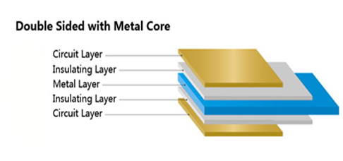
A double-sided metal PCB has a “copper-insulation-metal core-insulation-copper” sandwich structure. It is crucial to balance the copper layer area distribution, thickness, and track patterns on both sides to counteract internal stresses caused by different thermal expansion coefficients of copper and the metal core. This helps prevent severe warping during reflow soldering or operation.
Mechanical Stress and Mounting:
The metal PCB is typically fixed to the heatsink using screws. Sufficient copper-free zones around screw holes must be reserved to prevent short circuits and avoid track breakage due to mechanical stress. Additionally, the different thermal expansion coefficients of the metal base and heatsink must be considered, so elliptical holes or extra clearance are recommended for mounting holes.
Component Weight and Layout:
Heavy components (e.g., large electrolytic capacitors, transformers) should be positioned near mounting screws to avoid suspension, which could lead to solder joint fatigue due to long-term vibration. It’s also advisable to concentrate heavy components on one side.
4. Manufacturing and Processability (DFM)
Early Collaboration with Manufacturers:
Before finalizing the design, work closely with an experienced double-sided metal PCB manufacturer, such as PCBMASTER, to understand their process capabilities, material inventory, and design specifications. Gather specific parameters such as minimum line width/spacing, minimum via diameter, via spacing, copper thickness, insulation layer thickness, and filling materials.
File and Labeling:
In the Gerber files and design drawings, clearly label:
Which layers require electrical isolation from the metal core, and which (typically the ground network) should be connected to it.
Via processing requirements (e.g., via filling, plating).
The shape of the metal baseboard, slotting, and the non-conductive zone requirements around mounting holes.
Insulation layer thermal conductivity and voltage resistance ratings.
Key Considerations for Cutting and Shaping Double-Sided Metal PCBs and Engineering Documentation Optimization
The core structure of double-sided metal PCBs consists of a metal substrate, dual insulating thermal layers, and dual copper foils, offering excellent thermal conductivity and mechanical strength. However, due to the softness of the metal substrate, its tendency to deform, and the sensitivity of the bond between the insulation and metal layers, the cutting and shaping of these PCBs differ significantly from standard FR-4 boards. Below are the essential considerations for cutting and shaping double-sided metal PCBs, along with optimization strategies for engineering documentation.
1. Key Considerations for Cutting and Shaping Double-Sided Metal PCBs
When cutting and shaping double-sided metal PCBs, the focus should be on preventing metal substrate deformation, burrs, insulation layer cracking, and copper foil lifting. Common cutting methods include CNC milling, laser cutting, stamping, water jet cutting, and V-cut separation. The key considerations for each method are outlined below:
| Cutting Process | Best Use Cases | Risk Control Points | Not Suitable For |
| CNC Milling | Complex shapes, steps, slots, high precision | Layered cutting (≤0.8mm per pass), specialized aluminum-copper milling cutters, forced cooling (oil cooling preferred), bottom support | High-volume simple rectangles |
| Laser Cutting | Complex contours, thin boards (<2mm), no mechanical stress | N2/Ar assist gas, power gradient control, HAZ <0.1mm monitoring | Thick boards (>3mm), budget-sensitive |
| Water Jet Cutting | No heat impact required, medium thickness | Control sand particle size (80-120 mesh), adjust water pressure (300-400MPa), splash shields | Fine features (<0.5mm) |
| Stamping | High-volume, simple shapes | Precision progressive die design, step punching, edge pressure control | Small batches, prototype stage |
| V-Cut Separation | For straight pre-separation | Depth ≤ 60% of board thickness, leave connection bridges (0.5-1mm) | Final shapes, irregular boards |
2. General Process Control Points
Positioning and Deformation Prevention:
Use vacuum adsorption worktables instead of mechanical clamps to evenly distribute force and avoid damaging the metal substrate or causing local deformation.
When designing panelized boards, reserve a process edge (≥5mm width) and add positioning holes (diameter ≥2.0mm, at least two) to ensure alignment accuracy during milling or punching.
Avoid processing individual boards; instead, use panelization with a 0.8-1.0mm space between the boards to increase rigidity and reduce deformation.
Burr and Defect Control:
Burrs typically form on the metal substrate side; after milling, remove burrs with a brush and sandblasting (sandblasting pressure 0.2-0.3MPa) to ensure edge burr height ≤0.05mm.
Strictly control the distance between copper foil and the cutting edge: ensure that the copper foil edge is at least 0.2mm from the cutting edge to prevent stress-induced copper foil lifting.
Avoid sharp corners; all internal angles should be rounded with a radius of ≥0.3mm to prevent stress concentration, which can cause insulation layer cracking.
Post-Processing and Inspection:
After shaping, use ultrasonic cleaning (40kHz frequency) to remove any aluminum dust to avoid short circuits during subsequent soldering.
Key inspection points include:
Warping ≤0.5% (as per IPC-6012 standards).
No serrated edges.
No delamination or cracking in the insulation layer.
Copper foil adhesion meets standards (adhesion test using tape, no peeling).
3. Optimization of Engineering Documentation for Double-Sided Metal PCBs
Engineering documentation is the cornerstone for guiding production. To optimize the production process, it’s essential to address the specific material characteristics and process challenges of metal base PCBs. Engineering documentation should be optimized in four key areas: Gerber files, drawing annotations, process requirements, and compatibility design.
4. Gerber File Optimization: Enhancing Process Compatibility
Shaping Profile Precision Optimization:
Clearly indicate positive and negative tolerances on shaping profiles: As aluminum substrates are prone to deformation, the recommended shaping dimension tolerance is ±0.05mm (compared to the typical ±0.1mm for standard FR-4).
Use closed contour lines to prevent breakpoints or overlaps, which can cause tool misalignment during CNC milling.
In panelized designs, specify the milling path and panel separation sequence, milling internal contours first, then external contours, to reduce stress deformation on the substrate.
Fiducial and Alignment Mark Optimization:
Add optical fiducial marks: Each individual PCB should have at least two circular fiducial marks (diameter ≥1.0mm, exposed copper, no solder mask). For panelized designs, add global fiducial marks along the process edges to ensure precise alignment across drilling, component placement, and shaping processes.
Fiducial marks should be positioned at least 3mm away from the shaping edge to avoid damage during processing.
Copper Foil and Insulation Layer Boundary Optimization:
In the Gerber file, clearly define the copper foil coverage: Ensure that double-sided copper foils are fully adhered to the insulation layer with no exposed edges.
For thermal pads, mark the solder mask window size to ensure an unobstructed thermal path from the copper pads to the aluminum substrate and prevent solder mask coverage from interfering with soldering.
5. Drawing Annotation Optimization: Clearly Define Critical Technical Requirements
Material and Structural Annotation:
Clearly indicate the parameters for each layer of the aluminum substrate in the drawing: Aluminum material grade (e.g., 1060/6061), thickness (typically 1.0/1.5/2.0mm), insulation layer thickness (0.1-0.2mm), and copper foil thickness (13oz) to prevent material mix-ups during production.
Specify surface treatment requirements for the aluminum substrate, such as anodizing (5-10μm thickness) or passivation, to avoid oxidation that could affect heat dissipation.
Tolerance and Defect Standard Annotation:
Clearly define the warping and flatness requirements: Finished board warping should be ≤0.5%, and flatness ≤0.2mm/50mm to meet high-precision placement requirements for pick-and-place machines.
Provide defect judgment standards, such as edge burr height ≤0.05mm, no visible cracks in the insulation layer, and copper foil adhesion strength ≥1.0N/mm (per IPC standards).
Process Marking Annotation:
Add direction markings (e.g., arrow, PIN1 markings) to avoid incorrect assembly of double-sided PCBs.
Mark the location for board number, batch number, and production date in the silkscreen, and ensure the silkscreen is temperature-resistant (≥260°C) to avoid peeling during reflow soldering.
6. Process Requirements Optimization: Reducing Production Difficulty
Clearly Define Cutting and Shaping Process Plan:
Directly specify the process type, e.g., "Precision stamping for mass production, CNC milling for prototypes," to avoid the factory making its own process decisions that could reduce yield.
Specify deburring and cleaning requirements, such as "Milling must be followed by brush deburring and sandblasting, and ultrasonic cleaning for 10 minutes."
Surface Protection Optimization:
Require protective films on the aluminum substrate and copper foil surfaces before and after shaping, using PE protective film (thickness 0.05mm) to prevent scratches during processing.
Specify when to remove the protective film, e.g., "Remove protective film before component placement to avoid residue affecting soldering."
Panelization and Packaging Optimization:
When designing the panel, consider production efficiency: Adjust the number of boards in a panel according to the board size to ensure compatibility with production equipment.
Specify packaging methods: Use anti-static trays and vacuum packaging to prevent PCB deformation or static damage during transport.
7. Compatibility Design Optimization: Supporting Upstream and Downstream Processes
Compatibility with Drilling/Electroplating Processes:
Drill holes should be positioned at least 2mm away from the shaping edge to prevent deformation of hole walls during shaping.
Specify the copper plating thickness for metallized holes (≥25μm) to ensure good conductivity and heat dissipation.
Compatibility with Component Placement/Soldering Processes:
Design pads away from the shaping edge to prevent deformation during soldering, which could cause pads to lift.
Specify the reflow soldering temperature profile: Aluminum-based boards conduct heat quickly, so the holding time during reflow should be extended by 10-15 seconds compared to FR-4 boards to ensure full wetting of the solder.
Conclusion
The design, layout, and cutting of double-sided metal PCBs are critical to achieving optimal performance in high-power electronic applications. By carefully addressing key factors like electrical insulation, thermal management, and mechanical stress, and choosing the right manufacturing processes, engineers can ensure that these advanced PCBs meet the highest standards of reliability and efficiency. With the right approach, double-sided metal PCBs offer a powerful solution for next-generation electronics, combining superior heat dissipation, mechanical strength, and long-lasting performance.
FAQs
1. What are the primary benefits of using double-sided metal PCBs over traditional PCBs?
Double-sided metal PCBs offer improved thermal management, better mechanical strength, and higher reliability, especially in high-power electronic applications. They help dissipate heat more efficiently due to the metal core, reducing the risk of overheating. This makes them ideal for power electronics like LED drivers, power supplies, and automotive electronics, where heat dissipation and durability are critical.
2. How does thermal management differ in double-sided metal PCBs compared to traditional PCBs?
In double-sided metal PCBs, heat is more effectively transferred through the metal core, which acts as a heat sink. Unlike traditional PCBs, where heat may accumulate and affect performance, the metal core in double-sided designs enables more efficient heat distribution and dissipation. This is especially important when both sides of the board contain high-power components that generate significant heat.
3. What challenges are involved in the design of double-sided metal PCBs?
Designing double-sided metal PCBs requires balancing several factors, such as ensuring sufficient insulation between layers, managing thermal conductivity, and preventing mechanical stress. The design must carefully consider the dielectric properties and thickness of the insulation layer, as well as the potential for warping due to differential thermal expansion between the metal core and copper layers.
4. How do manufacturing processes like CNC machining or laser cutting impact double-sided metal PCBs?
Manufacturing processes like CNC machining, laser cutting, and water jet cutting are critical for achieving precision in double-sided metal PCBs. Each method has its own set of risks and advantages. For example, CNC machining is ideal for high-precision cuts and complex shapes, while laser cutting offers clean edges for thin boards. However, these processes must be carefully controlled to avoid damaging the layers, causing thermal stress, or leaving residual burrs that could affect PCB performance.
5. What are the best practices for ensuring the durability and longevity of double-sided metal PCBs?
To ensure the durability of double-sided metal PCBs, it's important to focus on high-quality materials and precision manufacturing. Using appropriate thermal interface materials, ensuring robust mechanical mounting, and optimizing the layout to prevent excessive thermal stress are all key. Additionally, regular testing for factors like warping, adhesion strength, and insulation quality is essential to guarantee that the PCB can withstand harsh operational conditions over time.
Author Bio
Hi, I'm Carol, the Overseas Marketing Manager at PCBMASTER, where I focus on expanding international markets and researching PCB and PCBA solutions. Since 2020, I've been deeply involved in helping our company collaborate with global clients, addressing their technical and production needs in the PCB and PCBA sectors. Over these years, I've gained extensive experience and developed a deeper understanding of industry trends, challenges, and technological innovations.
Outside of work, I'm passionate about writing and enjoy sharing industry insights, market developments, and practical tips through my blog. I hope my posts can help you better understand the PCB and PCBA industries and maybe even offer some valuable takeaways. Of course, if you have any thoughts or questions, feel free to leave a comment below—I'd love to hear from you and discuss further!