


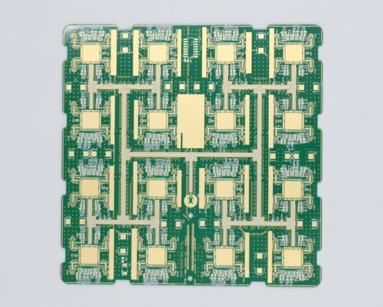
Why Capped Vias Are Essential for High-Density PCB Designs
As electronic devices get smaller and more powerful, the complexity of PCB (Printed Circuit Board) design has skyrocketed. To keep up with these demands, engineers are turning to innovative technologies that ensure reliability and performance. One such technology making waves in high-density interconnect (HDI) and fine-pitch designs is capped vias. By filling and sealing via holes, capped vias solve several challenges that traditional designs face, offering a more robust solution for high-speed, high-power applications. With the increasing need for miniaturization and top-tier performance, the advantages of capped vias are becoming clearer, positioning them as a key player in the evolution of modern electronics.
Capped Vias Definition and Core Functions
What Are Capped Vias?
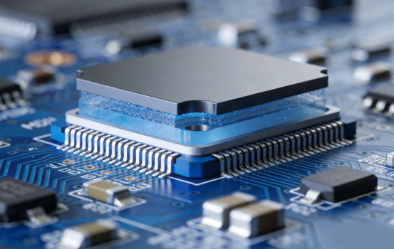
Capped vias are vias that are filled with a material like epoxy or copper paste and sealed with a layer of solder mask or copper. This process eliminates air gaps inside the via, preventing solder from flowing into the hole and improving heat transfer and signal integrity. Capped vias are commonly used in advanced PCB designs that require high precision, such as HDI designs.
How Do Capped Vias Solve Problems with Traditional Via Technologies?
Preventing Solder Wicking: Traditional vias can allow solder to flow into the hole, causing weak joints. Capped vias seal the hole, preventing this issue and ensuring stronger connections.
Reducing Signal Loss: Capped vias shorten the signal path, reducing signal degradation and improving performance, especially for high-speed applications.
Improving Heat Transfer: By using copper or other materials to fill vias, capped vias help dissipate heat more effectively, preventing overheating of power components.
Capped Vias' Role in High-Density Interconnect (HDI) Designs
Why Are Capped Vias Important for HDI Designs?
HDI designs require tightly packed components and fine-pitch connections. Traditional vias, like through-hole vias, take up too much space and can cause poor solder joints, reducing yield and reliability. Capped vias provide the following benefits for HDI:
Space Efficiency: Capped vias allow for smaller vias and denser component layouts, which is essential for high-density designs.
Better Soldering: Sealed vias create smooth, flat pads, improving the reliability of soldering fine-pitch components like BGAs.
Improved Signal Integrity: The sealed vias reduce parasitic inductance and signal loss, which is crucial for high-speed circuits.
Why Capped Vias Matter in Modern PCB Design
Capped vias enhance modern PCB designs in several key areas:
Miniaturization: They allow for smaller, more compact designs without sacrificing performance.
Reliability: Sealing via holes protects the PCB from moisture, dust, and heat, ensuring durability in harsh environments.
Thermal Management: Capped vias help dissipate heat more effectively, preventing component failure due to overheating.
Signal Quality: For high-speed applications like 5G, capped vias ensure minimal signal loss and better data transmission.
Capped Vias' Manufacturing Process: Filling and Sealing
Filling Step: Why Choose Epoxy Resin or Copper Paste?
The first key step in creating capped vias is the filling process. In this step, the via hole is filled with a material to eliminate air gaps and prepare it for sealing. The material chosen depends on the specific needs of the PCB:
1. Epoxy Resin: Epoxy is a non-conductive material commonly used to fill vias that carry signals. It provides excellent insulation, preventing unwanted electrical connections between different layers. Epoxy also helps prevent moisture and dust from entering the via, which could cause reliability issues.
2. Copper Paste: Copper paste is used when heat transfer or electrical conductivity is important. It is ideal for power vias, where high current or heat dissipation is necessary. Copper-filled vias improve the thermal management of the PCB by providing a better pathway for heat to flow away from critical components, preventing overheating and improving overall reliability.
By filling the via with either epoxy or copper paste, the hole is no longer just a hole—it becomes part of the structured, reliable path for signals or heat, depending on the application.
Sealing Step: How Is the Via Sealed with Copper or Solder Mask?
The second step in creating capped vias is the sealing process. After the via is filled, it is sealed to prevent contaminants, such as moisture or dust, from entering and to stop solder from wicking into the hole during assembly. Sealing is done using two methods:
1. Copper Sealing: A thin layer of copper is applied over the top of the via to create a smooth, flat surface. This method is typically used for power vias, where heat transfer and conductivity are important. Copper sealing also provides a more durable, long-lasting solution for harsh environments, where vibration or temperature extremes are a concern.
2. Solder Mask Sealing: For signal vias, a solder mask is often used to seal the via. The solder mask is a thin coating that is typically non-conductive and designed to block solder flow, preventing the solder from entering the via during the soldering process. This ensures that the PCB components are securely soldered without defects.
Both sealing methods effectively cap the via, preventing solder wicking and protecting the internal structure of the PCB, which is crucial for maintaining the integrity of the electrical connections.
Why Are Capped Vias Ideal for High-Frequency and High-Power Designs?
Capped vias are especially valuable in high-frequency and high-power designs for two main reasons: improved signal integrity and better heat management.
Impact of Capped Vias on Signal Integrity
How Do Capped Vias Improve High-Speed Signal Stability?
Capped vias play a crucial role in improving the stability of high-speed signals, especially those operating at frequencies above 1GHz. When a via is not filled and sealed, it can create a gap inside, leading to parasitic inductance and signal loss. These issues can significantly degrade the quality of the signal, particularly in high-speed applications.
By filling and capping the via, manufacturers can create a smooth, uninterrupted path for signals to travel through. This reduces parasitic inductance, which in turn minimizes signal attenuation (loss). For signals above 1GHz, even small losses can have a significant impact on performance. Capped vias ensure that these high-speed signals maintain their integrity, leading to more reliable data transmission and faster performance in applications like telecommunications and high-speed computing.
Advantages of Capped Vias in Applications Like 5G and PCIe
Capped vias are especially beneficial in applications that require high-frequency data transmission, such as 5G networks and PCIe interfaces. These technologies rely on the transmission of large amounts of data at very high speeds. In such applications, even minor disruptions to signal integrity can lead to failures or reduced performance.
For instance, in 5G systems, the demand for high-speed data transfer is immense, and even small signal losses can affect communication reliability. Capped vias help maintain a clean and efficient signal path, reducing losses and ensuring that the data transmitted remains accurate and stable.
Similarly, PCIe interfaces, used in high-speed computing environments, demand flawless signal transmission to ensure optimal performance. Capped vias help to minimize signal degradation, making them essential for these high-performance applications. By enhancing signal quality, capped vias improve the overall performance and reliability of 5G, PCIe, and similar systems.
Capped Vias' Role in Thermal Management
How Do Filled Materials Like Copper Improve Heat Transfer?
In power-sensitive PCBs, managing heat is a critical concern. Components such as voltage regulators or processors generate heat during operation, and if not managed properly, this heat can damage the components or degrade performance. Capped vias can help mitigate this problem, especially when filled with conductive materials like copper.
Copper-filled vias provide an excellent pathway for heat dissipation. Copper has a high thermal conductivity, meaning it can transfer heat away from sensitive components more efficiently than other materials. By filling the via with copper, heat can flow more easily through the PCB, preventing overheating and ensuring that components remain within safe operating temperatures. This helps protect the longevity and reliability of the board, especially in power-intensive applications like processors or power amplifiers.
How Do Capped Vias Compare to Traditional Vias in Thermal Performance?
When comparing capped vias to traditional vias, the difference in thermal performance becomes clear. Traditional vias, especially unfilled or partially filled ones, do not efficiently conduct heat. This inefficiency can lead to localized hot spots, which can cause damage to sensitive components or reduce their performance over time.
Capped vias, on the other hand, are designed with materials that enhance heat transfer. When copper is used for filling, the thermal conductivity improves significantly, making capped vias much more effective in preventing heat buildup. For example, a PCB with copper-filled capped vias will have better thermal performance compared to one with traditional unfilled vias, resulting in lower overall temperatures and better reliability in high-power environments.
The enhanced heat management provided by capped vias is especially important in applications that involve high currents, such as automotive electronics or power supplies, where heat can rapidly become a limiting factor in performance and reliability.
Impact of Capped Vias on PCB Manufacturing Costs
Capped vias add additional steps and materials to the PCB manufacturing process, which directly impacts the overall production costs. The extra work required to fill and seal the via holes increases the cost of the board. However, the long-term benefits—such as reduced assembly defects and higher performance—often justify the added expense, especially in high-density and high-performance designs.
Additional Costs of Filling and Sealing: How Do They Affect Overall PCB Manufacturing Price?
The process of creating capped vias involves two main steps: filling and sealing. These extra steps—compared to traditional via types—introduce additional costs to the manufacturing process. Typically, these additional costs range from 10% to 20% higher than the production costs for traditional vias.
1. Filling the Vias: The via holes must be filled with either epoxy (for insulation) or copper paste (for thermal or electrical conductivity). This filling material is an additional cost. Copper paste, in particular, is more expensive than other materials, which contributes to the higher cost of capped vias.
2. Sealing the Vias: After the vias are filled, they are sealed with a solder mask or copper layer. This requires extra processing time and materials, adding to the cost of production. Solder mask sealing is relatively inexpensive, but copper sealing, which provides better heat management and conductivity, raises costs further.
While these added steps increase the initial price of the PCB, they result in a more reliable and durable board, which can reduce long-term costs related to failures and reworks.
How Can Reduced Assembly Defects and Improved Yield Offset These Additional Costs?
Though capped vias increase the upfront cost of manufacturing, they contribute significantly to the reliability and performance of the finished PCB. This, in turn, can reduce costs in other areas, particularly during assembly and the later stages of production. Specifically, capped vias help to:
1. Reduce Assembly Defects: During assembly, unsealed vias can cause issues like solder wicking, where solder flows into the via instead of staying on the pad. This can lead to weak joints, poor soldering, or component misalignment. Capped vias prevent this by sealing the via and providing a flat, even surface for soldering. As a result, there are fewer defective boards, reducing the need for rework and scrap.
2. Increase Yield: Because capped vias help maintain the integrity of solder joints, they increase the likelihood of successful assembly on the first attempt. This leads to a higher yield during PCB production, which compensates for the extra costs. A higher yield means fewer failed units, less rework, and fewer resources spent on testing and repairs.
In the long run, these improvements in assembly quality can offset the added costs of capped vias, especially in high-performance, high-reliability designs where performance is critical.
Cost-Effectiveness of Capped Vias
Capped vias offer long-term value, particularly in designs that require HDI or operate at high frequencies and power levels. While capped vias increase the initial cost of manufacturing, they provide cost-effective solutions in specific design scenarios where reliability and performance are paramount. Let’s explore how this value plays out over time.
Long-Term Cost-Effectiveness in High-Density and High-Performance Designs
In designs with HDI, such as smartphones, wearables, or advanced computing devices, space is limited and components are smaller and packed more closely together. Capped vias play a crucial role in enabling compact designs while maintaining performance. Here's how they contribute to long-term cost-effectiveness:
1. Reduced Risk of Failure: In HDI designs, small vias are essential to connect various PCB layers. Capped vias prevent common issues like solder wicking, signal loss, or heat buildup, all of which can lead to PCB failure. A failure in an HDI PCB can be very costly to repair, often requiring the replacement of an entire device or component. Capped vias help mitigate these risks, reducing the likelihood of such costly failures.
2. Enabling Advanced Features: High-performance designs, such as those used in 5G or PCIe applications, require more precise and reliable connections. Capped vias provide the necessary stability and signal integrity to support these demanding technologies. The upfront cost of capped vias is justified by the enhanced capabilities they bring, enabling the design to support more complex functions and higher speeds.
3. Fewer Reworks and Downtime: With capped vias improving signal and thermal management, manufacturers can experience fewer failures during production and assembly. This leads to fewer rework cycles and less downtime, ultimately reducing the operational costs associated with defective boards.
Thus, while capped vias increase the initial cost, their use in high-density and high-performance designs leads to more reliable, longer-lasting PCBs that deliver value over time.
Applications That Gain the Most from Capped Vias
HDI Designs: Supporting Micro BGA/QFN Packages
Capped vias are particularly advantageous in HDI designs. These designs feature tightly packed components and are used in advanced electronics like smartphones, wearables, and other compact devices.
1. Micro BGA (Ball Grid Array) and QFN (Quad Flat No-lead) Packages: These components, which are commonly used in HDI designs, have very small pads that require precise soldering. Without capped vias, solder can wick into the via, leaving the pad empty and causing poor solder joints. Capped vias provide a flat surface, ensuring that solder stays on the pad, preventing misalignment or weak joints.
2. Space Efficiency: HDI designs often use microvias to create connections between layers, which allows for more compact layouts. Capped vias help reduce issues like signal loss and soldering defects, ensuring that the smaller vias still perform well in high-density designs.
By providing flat surfaces and preventing solder flow into vias, capped vias improve the reliability of these advanced components, making them an essential part of HDI designs.
High-Stress Environments: Durability in Automotive, Aerospace, and Medical Applications
In high-stress environments, such as those found in automotive, aerospace, and medical industries, the reliability and durability of a PCB are critical. Capped vias can withstand extreme conditions like temperature fluctuations, moisture, and vibration, making them ideal for these applications.
1. Automotive Electronics: Components in automotive systems, such as engine control units (ECUs) and sensors, must endure harsh conditions. Capped vias provide an extra layer of protection, preventing moisture, dust, and other contaminants from entering the via and compromising the PCB’s performance. Sealed vias also improve thermal management, which is crucial in automotive applications where heat is a major concern.
2. Aerospace: Aerospace electronics must function reliably under extreme pressure changes, vibration, and temperature extremes. Capped vias provide the durability needed to survive in these environments, reducing the risk of failure in mission-critical systems.
3. Medical Devices: Medical devices, particularly implantable ones, require a high level of reliability and durability. Capped vias protect against environmental factors like moisture or temperature shifts, ensuring that the PCB in devices like pacemakers or hearing aids continues to function without issue.
The sealed nature of capped vias makes them an excellent choice for these high-stress industries, where failure is not an option.
Are Capped Vias Suitable for Low-Density, Low-Cost Designs?
Capped vias, while beneficial, come with additional costs due to the filling and sealing processes. As a result, they may not always be the most economical choice for low-density, low-cost designs.
Can Low-Cost PCB Designs Ignore the Additional Costs of Capped Vias?
For simple PCBs, such as those used in basic consumer electronics or low-density designs, the benefits of capped vias may not justify the additional cost. In these cases, traditional via types like through-hole vias, blind vias, or buried vias may be sufficient.
Through-Hole Vias: These vias are the most common and least expensive type. They are suitable for simple PCBs where space and performance demands are not as stringent. They do not require the extra steps of filling and capping, making them more cost-effective.
Blind and Buried Vias: These vias are more suitable for medium-density designs where saving space is more critical than ensuring high-frequency performance or reliability under harsh conditions. They can also be produced at a lower cost than capped vias.
In low-cost designs, where minimizing production expenses is essential, capped vias may not provide enough return on investment. Traditional via types will suffice, especially when there is less need for the enhanced performance that capped vias offer.
Comparison of Capped Vias vs. Traditional Vias
| Via Type | Cost | Suitability | Benefits | Drawbacks |
| Capped Vias | Higher (10–20% more) | Not ideal for low-cost, low-density designs | - Improved signal integrity - Better thermal management - Sealed for higher reliability | - Additional steps (filling and sealing) increase manufacturing cost - Not cost-effective for simple designs |
| Through-Hole Vias | Lowest cost | Best for low-density, basic consumer electronics | - Simple and cost-effective - Strong mechanical connection | - Takes up more space - Prone to solder wicking and signal loss in high-density or high-speed applications |
| Blind Vias | Moderate cost | Suitable for medium-density designs | - Saves PCB space - Shorter paths reduce signal loss compared to through-hole vias | - Does not prevent solder wicking - No sealing, potential for moisture ingress |
| Buried Vias | Moderate cost | Best for medium-density designs | - Saves space for more compact designs - No exposure to outer layers | - Cannot be inspected easily - No thermal benefits or sealing, limiting performance in demanding applications |
Key Takeaways:
Capped vias are not the best choice for low-cost, low-density designs due to their higher manufacturing costs.
Through-hole vias are ideal for basic designs, offering low cost and reliability but sacrificing space efficiency and performance in high-speed applications.
Blind and buried vias are good for medium-density designs, balancing cost and performance but still lack the benefits of capped vias in terms of sealing and thermal management.
Manufacturing Challenges of Capped Vias and Solutions
Capped vias are a critical component of modern PCB designs, offering numerous benefits like improved reliability and better thermal management. However, their manufacturing process can present several challenges. Let’s explore these common issues and the solutions that help ensure capped vias maintain high quality and performance.
Common Quality Issues in Capped Via Production and How They Affect Reliability
1. Filling Voids and Incomplete Filling
One of the most common issues when producing capped vias is voids in the fill material. Voids occur when air pockets or incomplete filling remain inside the via after the filling process. This can compromise the via's electrical and thermal conductivity, leading to potential failure in high-performance or high-stress environments.
Impact on Reliability: Voids can lead to weak electrical connections, affecting signal integrity and heat transfer. In extreme cases, voids may cause complete failure in the PCB, especially under thermal cycling or high-frequency signal conditions.
2. Surface Irregularities (Dimples or Depressions)
Another challenge is surface irregularities, such as dimples or depressions that can occur on the via cap during the planarization process. These imperfections are problematic because they prevent the solder from adhering properly to the PCB during assembly, which can result in weak solder joints and potential defects in the final product.
Impact on Reliability: Dimples or depressions in the via cap can lead to misalignment during component soldering, causing poor electrical contact, solder defects, or even component failure due to poor joint quality.
3. Misalignment or Displacement
Misalignment or displacement can happen during the drilling or capping process, especially when the via is not perfectly aligned with the PCB layers. Misalignment can result in poorly connected layers, leading to short circuits or open circuits.
Impact on Reliability: Misaligned vias can cause signal integrity issues, as well as thermal problems due to poor heat transfer between layers. This can also result in mechanical stress on the PCB, increasing the likelihood of cracking or failure over time.
How to Reduce Manufacturing Issues Using Advanced Equipment and Technology
1. Vacuum-Assisted Filling to Prevent Voids
To tackle the issue of filling voids, vacuum-assisted filling is often used. This method involves applying a vacuum to remove air pockets from the via before the fill material (such as epoxy or copper paste) is injected. The vacuum ensures that the fill material completely fills the via, reducing the likelihood of voids forming.
Benefits: Vacuum-assisted filling results in consistent and complete filling, which improves signal and thermal conductivity. This ensures better electrical performance and heat management, crucial for high-frequency and high-power applications.
2. Laser Drilling for Precision
Using laser drilling helps achieve greater precision in creating microvias, especially for HDI (high-density interconnect) designs. Laser drills can create smaller vias with higher accuracy compared to traditional mechanical drills. This precision reduces the likelihood of misalignment and ensures that vias are perfectly positioned.
Benefits: Laser drilling ensures that vias are perfectly aligned with the PCB layers, leading to better electrical connections and avoiding issues like misaligned pads or displaced vias. This process helps improve overall PCB reliability.
3. Automated Optical Inspection (AOI)
Automated Optical Inspection (AOI) is a key technology used in the inspection of via caps. AOI systems can detect surface irregularities like dimples or misalignments with high precision. These systems use high-resolution cameras to inspect the vias in real time, ensuring that only high-quality vias are passed onto the next stage of production.
Benefits: AOI ensures that the cap flatness and via alignment meet the required standards, significantly reducing defects during assembly and increasing the overall reliability of the PCB. This is particularly important in ensuring the soldering quality for fine-pitch components.
Ensuring High-Quality Capped Vias in the Production Process
1. Adhering to IPC 4761 Type VII Standards
To ensure consistent quality in capped vias, manufacturers must strictly adhere to industry standards, such as IPC 4761 Type VII, which provides detailed guidelines for via filling and capping. These standards specify the acceptable cap thickness, via fill material properties, and the tolerances for flatness.
Key Aspects of IPC 4761 Type VII:
Cap Thickness: Ensures that the cap is thick enough (typically between 10–20μm for solder mask caps or 5–10μm for copper caps) to prevent contamination and allow for proper soldering.
Fill Material: The fill material (such as epoxy or copper paste) must meet certain conductivity and mechanical strength requirements to maintain the reliability of the PCB.
Flatness: The cap surface must remain flat with a deviation no greater than ±2μm to ensure smooth soldering and reliable connections.
Adhering to these standards ensures the reliability and durability of the capped vias, reducing the risk of defects that could lead to failure in the finished product.
2. Consistent Process Control and Testing
Besides adhering to IPC standards, manufacturers should implement process control at every stage of production to ensure high-quality capped vias. This includes tight monitoring of filling processes, plating thickness, via alignment, and cap application.
Benefits: By maintaining tight control over the production process, manufacturers can reduce the chances of defects like voids, misalignment, or surface irregularities. Regular testing (such as X-ray inspection to detect voids and AOI to inspect cap flatness) ensures that only vias meeting quality standards make it through to the final product.
Conclusion
When deciding whether to use capped vias in your PCB design, the key factor is the complexity and performance requirements of your project. Capped vias are ideal for high-density designs, such as those with fine-pitch packages like BGAs or QFNs. They are also essential for designs that need excellent thermal management and signal integrity, such as 5G, PCIe, and high-performance electronics.
However, capped vias may not be necessary for simpler, low-density designs where budget constraints are a priority. For these types of PCBs, traditional vias like through-hole or blind/buried vias offer a more cost-effective solution without sacrificing performance for basic applications.
In summary, choose capped vias when you need enhanced reliability, reduced signal loss, and improved heat dissipation, particularly for complex or high-performance applications. If you're working with a budget or on simpler designs, traditional via technologies will suffice.
If you have more questions or need further guidance on PCB design, feel free to reach out to PCBMASTER. As a professional PCB supplier, we are here to provide expert advice tailored to your specific needs.
FAQs
How Do Capped Vias Improve Signal Integrity?
Capped vias enhance signal integrity by minimizing the parasitic inductance and reducing signal attenuation. In traditional vias, the hole in the PCB can act as an antenna, increasing inductance and causing signal loss, especially at high frequencies. By filling the via and capping it, the surface becomes smooth and even, reducing the distance signals must travel and preventing the loss of high-speed signals. Capped vias effectively shorten signal paths, making them ideal for high-frequency applications such as 5G and PCIe, where every bit of signal integrity matters. This results in improved transmission quality, ensuring reliable data flow even at speeds above 1 GHz.
What Is the Production Cost of Capped Vias?
The production cost of capped vias is higher than traditional via technologies due to the additional steps involved, such as filling the vias with materials like epoxy or copper and applying a protective cap. These processes add about 10–20% to the overall cost of the PCB. However, this added expense can be offset by the reduction in assembly defects and the increase in reliability, which lowers the likelihood of rework or failures in the final product. Capped vias enhance the quality of HDI designs, where precision and performance are critical. Therefore, while the initial cost is higher, the long-term benefits of fewer defects and improved product performance often make them a worthwhile investment.
Can Capped Vias Be Used in Flexible PCBs?
Yes, capped vias can be used in flexible PCBs. The process for creating capped vias in flexible PCBs is similar to rigid PCBs, but with additional care to maintain the flexibility of the substrate. The filled via provides rigidity to critical areas, such as connector pads or areas with high current flow, without compromising the overall flexibility of the PCB. By using materials like polyimide for the flexible substrate and epoxy for the via fill, manufacturers can create reliable and durable flex PCBs suitable for applications like wearable devices and flexible displays. This combination ensures that the PCB performs well in both flexibility and reliability, making it ideal for demanding applications.
Do Capped Vias Effectively Prevent Solder Wicking?
Yes, capped vias are highly effective in preventing solder wicking, a common issue during PCB assembly. Solder wicking occurs when solder flows into the via holes, which can create weak solder joints and potential short circuits. Capped vias solve this problem by sealing the via hole with a flat, smooth surface—either through a solder mask or copper plating—preventing the solder from flowing into the via. This results in cleaner, more reliable solder joints, especially for fine-pitch components like BGAs and QFNs, which are sensitive to soldering defects. The sealed vias reduce the risk of misalignment and improve the overall quality of the soldering process, ensuring a more robust and long-lasting connection.
What Is the Difference Between Capped Vias and Via-in-Pad (VIP)?
The main difference between capped vias and via-in-pad (VIP) lies in the way the vias are handled during assembly. In via-in-pad designs, the via is placed directly under the component pad, which often requires additional steps like tenting (covering the via with a solder mask) or capping to prevent solder from flowing into the via. However, VIPs can still face the risk of solder mask peeling, which leads to solder wicking.
On the other hand, capped vias provide a more secure and reliable solution by fully sealing the via with a flat cap, either a copper or solder mask, ensuring that no solder can enter the via during assembly. Capped vias provide better reliability in the long term since the sealed via reduces the risk of defects like misalignment and poor solder joints. While VIPs can offer space savings and are common in high-density designs, capped vias are generally more dependable for preventing soldering issues and improving the final product’s quality, particularly in high-reliability applications.
Author Bio
Hi, I'm Carol, the Overseas Marketing Manager at PCBMASTER, where I focus on expanding international markets and researching PCB and PCBA solutions. Since 2020, I've been deeply involved in helping our company collaborate with global clients, addressing their technical and production needs in the PCB and PCBA sectors. Over these years, I've gained extensive experience and developed a deeper understanding of industry trends, challenges, and technological innovations.
Outside of work, I'm passionate about writing and enjoy sharing industry insights, market developments, and practical tips through my blog. I hope my posts can help you better understand the PCB and PCBA industries and maybe even offer some valuable takeaways. Of course, if you have any thoughts or questions, feel free to leave a comment below—I'd love to hear from you and discuss further!

