


PCB Stackup Design: The Cornerstone of High-Performance Circuit Boards – A Comprehensive Guide and Best Practices
Introduction
Within the field of electronic product design, the importance of PCB (Printed Circuit Board) stack-up design is often underestimated. When outputting manufacturing files, many design teams often fill their drawings with over-constrained dimensions, use non-standard parameters, or even determine the number of layers and thickness based on "educated guesses." More commonly, submitted stack-up specifications lack critical data, forcing manufacturers to fill in the technical gaps – while reliable manufacturers can usually handle this, such an approach undoubtedly increases project risk.
Whether for simple consumer electronics or complex high-speed communication equipment, an excellent stack-up design can significantly enhance the long-term reliability of the circuit board, optimize signal performance, reduce production costs, and accelerate time-to-market.
What is a PCB Stack-up? An In-Depth Analysis of Its Core Value
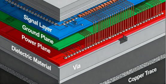
A PCB stack-up is a strategic plan created before the circuit board layout. This “blueprint” defines the structural arrangement and material configuration of the board’s layers, detailing the sequence, thickness, and materials of the conductive layers (copper foil) and insulating layers (dielectric material), which is crucial for the electrical, mechanical, and thermal properties of the board. In the context of printed circuit boards, the layer stack and layer stackup refer to the specific arrangement and distribution of layers in multilayer PCBs, directly impacting signal integrity, manufacturability, and overall board performance.
Stack-up design is not just about electrical connectivity; it is key to achieving the following objectives:
·Control characteristic impedance and ensure signal integrity (SI).
·Manage power distribution and reduce noise interference.
·Optimize thermal management and increase power density.
·Suppress electromagnetic interference (EMI) and pass relevant certifications.
·Balance cost and performance to meet budget requirements.
PCB Stack-up Details: From Material Selection to Thickness Planning
Copper Weight Selection:
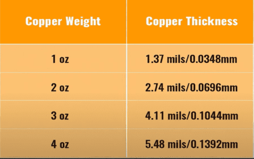
PCB copper layer thickness typically ranges from ½ ounce (approx. 18μm) to 2 ounces (70μm) or more. Copper thicknesses can vary across different PCB types and layers; in multilayer designs, layer copper thickness and inner layer copper thickness are key parameters that must be specified for both performance and manufacturability. The selection is based on:
·Current carrying capacity (power density).
·Impedance control precision (for high-speed signals).
·Heat dissipation requirements (for high-power applications).
Basic Material Composition:
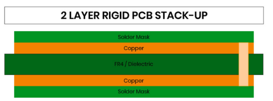
·Single-sided boards: Simple structure, containing substrate, copper foil, solder mask, and silkscreen layers.
·Multi-layer boards: Complex structure, containing multiple signal layers, plane layers, bonded together using prepreg and core materials. Copper pours are often used in these designs, which can impact overall board thickness and introduce manufacturing constraints that should be coordinated with the fabricator.
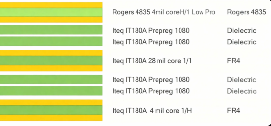
Prepreg, as the interlayer adhesive material, has resin flow characteristics critical to lamination quality. The resin system used in the prepreg is also important, as it determines the electrical and mechanical properties of the finished PCB. The core provides mechanical support and electrical insulation. For high-layer-count, high-speed, or high-frequency boards, material selection (such as low-loss FR-4, Rogers materials, etc.) directly impacts final performance.
The total thickness of the PCB is determined by the combination of all copper and dielectric layers, and is a critical parameter for both design and manufacturing.
Stack-up Design Strategies for Advanced PCB Technologies
As electronic devices evolve towards higher performance and miniaturization, specialized stack-up design solutions become increasingly important.
1.Metal Core PCB (MCPCB) Stack-up Design
·Application Scenarios: High-power LED lighting, automotive electronics, power modules.
·Design Key Points: The metal core (usually aluminum or copper) handles the primary heat dissipation task. A balance between the thermal conductivity of the dielectric layer and the thickness of the metal core must be considered.
2.HDI (High-Density Interconnect) Stack-up
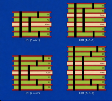
·Technical Characteristics: Utilizes microvias, blind vias, and buried vias to achieve high wiring density. In high-density designs, the use of ball grid array (BGA) and BGA components is common, which increases component density but also impacts layer count and routing complexity due to high pin counts and tighter space constraints.
·Stack-up Schemes: Can employ any-layer interconnect (ELIC) or staggered via-in-pad designs to meet the space constraints of portable devices.
3.High-Frequency/RF Circuit Stack-up
·Key Parameters: Dielectric constant (Dk) stability, loss tangent (Df), and surface roughness.
·Special Considerations: Impedance continuity along the RF signal path, and coplanar waveguide design with grounding. Differential pair routing is critical for maintaining signal integrity at high frequencies and for high frequency signals, helping to control skew and minimize losses. Avoiding impedance mismatch is essential to prevent signal reflection and maintain overall circuit reliability. Maintaining minimal spacing between conductive layers is also necessary to meet design and safety requirements, especially in high-frequency and multilayer designs.
4.Flexible/Rigid-Flex PCB Stack-up
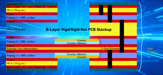
·Structural Innovation: Combines the stability of rigid sections with the dynamic bending capability of flexible sections.
·Material Selection: Polyimide substrates provide heat resistance and flexibility, while coverlays protect the circuit structures. For high-speed signals, the next layer adjacent to the signal trace should serve as a solid reference plane, ensuring a stable return path and minimizing signal distortion.
Multilayer PCB designs require careful PCB stackup design, including the arrangement of one layer over another, the use of power layer and signal layer, and the importance of routing layers and trace width for signal integrity. Standard PCB stack-ups typically use two outer layers for signal or power distribution, and the power supply network must be integrated into the stack-up to ensure reliable power delivery and noise reduction.
Ground Layer and Plane Design: Foundations for Signal Integrity and Power Distribution
A robust ground layer and well-designed ground planes are the backbone of any high-performance pcb stack up. In multilayer pcbs, a solid ground plane—often placed on an inner layer—serves as a stable reference for all signal layers, dramatically improving signal integrity and reducing the risk of electromagnetic interference (EMI). By providing a continuous, low-impedance path for return currents, the ground plane minimizes voltage fluctuations and supports the reliable operation of high speed circuits.
When planning your stack up, it’s essential to allocate sufficient copper thickness to the ground layer, ensuring it can handle the return currents without excessive voltage drop. The placement of ground and power planes should be carefully coordinated with signal layers to create effective reference planes for controlled impedance traces, especially in high speed and high frequency designs. Increasing the layer count to include dedicated ground and power planes can further enhance noise immunity and power distribution, while optimizing dielectric thicknesses between layers helps maintain target impedance and suppress crosstalk.
For best results, maintain a solid ground plane beneath critical signal traces and avoid unnecessary splits or voids in the ground layer. This approach not only supports good signal integrity but also simplifies the design of power delivery networks and improves overall electromagnetic compatibility. Thoughtful ground and power plane design is a key differentiator in achieving reliable, high-performance circuit boards.
Five Key Factors Determining the Stack-up Scheme
1. Lamination Process: Foil Lamination vs. Cap Lamination
·Foil Lamination (Recommended): Uses copper foil for the outer layers; lower cost, higher registration accuracy.
·Cap Lamination: Uses core material for the outer layers; only suitable for special materials or when specific process limitations exist.
In multilayer PCB construction, the lamination process directly impacts the electrical characteristics and assembly of the inner layers, making their quality and consistency critical for overall board performance.
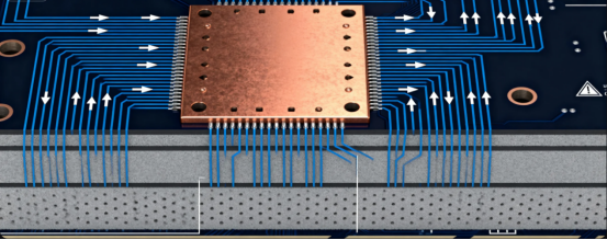
2. Component Density and Pin Count
·Fine-pitch BGAs (e.g., below 0.65mm pitch) typically require more signal layers for fan-out routing.
·High-pin-count devices (e.g., FPGAs with 1000+ pins) require comprehensive consideration of the Power Delivery Network (PDN) and signal routing. Proper arrangement of ground layers is essential to optimize electrical performance and manufacturability in dense designs.
3. Circuit Type and Signal Speed
·Analog Circuits: Require a focus on shielding and grounding to reduce noise coupling.
·High-Speed Digital Buses (e.g., DDR4/5, PCIe): Demand strict impedance control and uninterrupted reference planes.
·Mixed-Signal Systems: Manage digital-to-analog interference through ground partitioning and isolation moats.
Proper stack-up design can also minimize susceptibility to external noise, improving electromagnetic compatibility and reducing interference that affects signal integrity.
4. Thermal Management Requirements
·High-power designs may require increased copper thickness or dedicated thermal conduction layers.
·Consider Coefficient of Thermal Expansion (CTE) matching to avoid long-term reliability issues.
5. Mechanical and Spatial Constraints
·Board thickness may be limited by connector specifications or housing dimensions.
·Thin designs (e.g., 0.4mm) require assessment of mechanical strength and compatibility with assembly processes.
PCB Fabrication Process: Bridging Design and Manufacturing

The journey from schematic to finished printed circuit board relies on a well-orchestrated pcb fabrication process, where the initial pcb stack up definition sets the stage for success. The process begins with the creation of a detailed stack up, specifying the arrangement of signal layers, power and ground planes, and insulating layers. This stack up is translated into comprehensive fabrication notes, which guide the manufacturer through each production step.
Material selection is a critical early decision—choosing the right copper foil, core material, and prepreg ensures the board meets electrical and mechanical requirements. The fabrication process includes precise cutting, drilling (including blind vias for high density interconnect designs), and copper plating to achieve the desired copper weight and layer thickness. Each layer is carefully laminated, with attention to maintaining consistent copper thickness and dielectric thicknesses throughout the pcb stack.
Copper plating and etching define the intricate patterns of signal layers and power planes, while strict process controls ensure that the final board matches the specified stack up and meets all performance criteria. By understanding the interplay between design choices and manufacturing realities, designers can create stack ups that are both high-performing and manufacturable, reducing the risk of costly revisions and ensuring a smooth transition from design to production.
PCB Stack-up Design Best Practices: A Six-Step Workflow
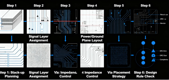
·Preliminary Requirements Analysis: Define signal speeds, power levels, environmental conditions, and cost targets.
·Layer Count Estimation: Preliminary determination of the number of layers based on pin density, available routing channels, and power network complexity.
·Stack-up Planning: Use professional tools (e.g., Polar Si9000) for stack-up modeling and impedance calculation.
·Material Selection: Choose appropriate substrate and copper foil types based on electrical, thermal, and mechanical requirements.
·Manufacturer Communication: Confirm process capabilities and material availability with the PCB supplier early in the design process.
·Design Verification: Validate the stack-up through simulation (SI/PI) and prototype testing.
Common Stack-up Design Pitfalls and Avoidance Strategies
Pitfall 1: "Fewer layers always mean lower cost."
Reality: Unreasonable reduction of layers can lead to performance degradation or redesigns, potentially increasing the total cost.
Pitfall 2: Neglecting the impact of manufacturing tolerances.
Solution: Impedance calculations must account for process variations in copper thickness, dielectric thickness, and dielectric constant.
Pitfall 3: Finalizing the stack-up at the last minute.
Optimal Timing: Lock down the stack-up scheme before starting the component layout to avoid major modifications later.
Circuit Board Applications: Tailoring Stack-up Choices to Real-World Needs
Every circuit board application brings its own set of challenges, making it essential to customize the pcb stack up to fit specific requirements. For high speed digital systems, the stack up must support good signal integrity by minimizing signal latency, controlling impedance, and providing robust power delivery. This often involves increasing the layer count, optimizing copper thickness, and carefully selecting dielectric thicknesses to achieve the desired electrical performance.
Analog and mixed-signal designs, on the other hand, may prioritize noise reduction and stable voltage references, requiring thoughtful placement of ground planes and the use of specialized materials to suppress electromagnetic interference. High frequency and RF applications demand stack ups with low-loss dielectrics and precise layer spacing, sometimes leveraging advanced fabrication techniques like laser drilling to accommodate complex geometries and tight tolerances.
Thermal management, power delivery, and mechanical constraints also influence stack up choices. For example, boards used in power electronics may require thicker copper layers and additional plane layers to handle higher currents, while compact consumer devices might benefit from high density interconnect stack ups with minimal board thickness.
By aligning stack up design with the unique demands of each circuit board application, designers can ensure reliable operation, meet stringent performance standards, and take full advantage of the latest materials and manufacturing technologies. Whether you’re developing a high speed communication device or a precision analog sensor, a tailored stack up is the key to unlocking your product’s full potential.
Conclusion: Stack-up Design is a Systems Engineering Task
PCB stack-up design sits at the intersection of electrical performance, thermal management, mechanical structure, and manufacturing cost. A successful stack-up scheme requires close collaboration between design engineers and manufacturers to find the optimal balance under multiple constraints. Through systematic stack-up planning, you can not only enhance product performance and reliability but also shorten development cycles, ultimately gaining a competitive edge in the market.
Recommended Next Steps: When starting your next PCB design project, consider re-evaluating the stack-up plan using the framework introduced in this article. Share your stack-up requirements with your manufacturer and leverage their experience to optimize the design. To further discuss stack-up strategies for specific applications, please feel free to contact our technical team for customized solutions.
FAQs
Q. What is PCB Stackup?
A. It refers to the layered arrangement of copper foils (signal layers, power layers, ground layers) and dielectric layers (substrate) in a PCB. It determines the electrical performance (such as impedance, signal integrity), heat dissipation capability, and mechanical strength of the PCB, and is the core foundation of PCB design.
Q. What are the common types of PCB Stackups?
A. Core types classified by layer count:
·Double-layer board: 2 copper layers (top + bottom), suitable for simple circuits (e.g., toys, small appliances).
·Four-layer board: 4 copper layers (top signal + internal power + internal ground + bottom signal), balances performance and cost, widely used in consumer electronics.
·Six-layer and above multi-layer boards: contain multiple signal layers + dedicated power/ground layers, used for high-speed signals (e.g., 5G equipment, servers).
Q. When designing a PCB Stackup, why is it important to prioritize dedicated power and ground layers?
A. Dedicated power/ground layers can:
·Reduce power impedance and minimize voltage fluctuations.
·Provide a "low-impedance return path" for signals, reducing signal interference.
·Disperse heat, improving thermal efficiency.
·Simplify routing, avoiding interference between power/ground traces and signal traces.
Q. How does the Stackup of an HDI PCB differ from that of a standard PCB?
A. HDI stackups place greater emphasis on "high-density interconnects":
·Use thinner dielectric layers (typically ≤0.1mm), reducing interlayer spacing.
·Incorporate microvias and stacked vias to achieve flexible interlayer connections.
·Often feature "asymmetric stackups" (e.g., top signal + internal microvia layer + ground layer) to suit small form factor requirements, whereas standard PCBs primarily use symmetric stackups.
Q. How is the "dielectric material" selected in a Stackup?
A. Selection must match the application scenario:
·General scenarios (e.g., mobile phones): Choose FR-4 (Tg≥130°C), low cost and mature process.
·High-speed/high-frequency scenarios (e.g., routers): Choose high-frequency substrates (e.g., Rogers 4350) to reduce signal loss.
·High-temperature scenarios (e.g., automotive engine compartments): Choose high Tg FR-4 (Tg≥170°C) or ceramic substrates for superior temperature resistance.
Q. Does PCB Stackup design affect impedance control? How to match?
A. Yes. Impedance is determined collectively by "trace width, copper thickness, dielectric thickness / dielectric constant." During design, it is necessary to:
·Determine parameters based on signal requirements (e.g., 50Ω single-ended impedance, 100Ω differential impedance.
·Use impedance calculation tools (e.g., Polar SI9000) to verify stackup parameters, ensuring impedance deviation is ≤ ±10%.
Q. What should be noted when setting the "layer spacing" during stackup?
A.
·Spacing between signal layer and ground layer: Should be small (e.g., 0.1-0.2mm) to enhance shielding and reduce signal interference.
·Spacing between power layer and ground layer: Should be small to reduce power impedance.
·Spacing between high-frequency signal layers: Needs adjustment considering the dielectric constant to avoid signal crosstalk, typically ≥0.2mm.
Q.How to judge if an existing Stackup is reasonable?
A.
Key checks include:
·Whether signals have independent return paths (no "floating signals").
·Whether power/ground layers cover critical heat-generating components.
·Whether high-speed signal layers are isolated from noise sources (e.g., power layers);
·Whether actual impedance testing and signal eye diagrams meet design requirements.
Author: Jack Wang

