


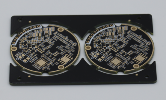
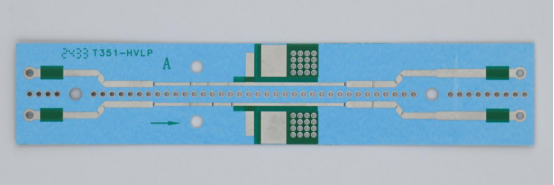
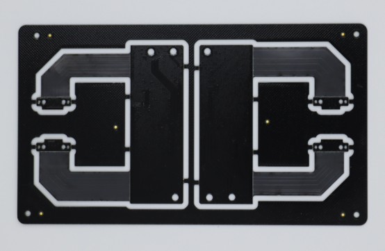
2-Layer Aluminum Base PCBs:Manufacturing Challenges and Solutions
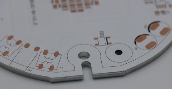
2-layer aluminum base PCBs (Printed Circuit Boards) are essential components in modern high-power electronics. They are widely used in applications like LED lighting, electric vehicle (EV) power modules, and industrial controllers due to their superior heat dissipation properties. Unlike traditional FR-4 PCBs, aluminum base PCBs are designed to conduct heat away from sensitive components, ensuring reliable performance in high-power environments.
However, manufacturing these PCBs comes with significant challenges. The bond between the aluminum base and dielectric layer is critical, yet it can fail due to material incompatibility or poor process control. Additionally, selecting the right resin to handle thermal cycling and ensuring solder mask adhesion are key hurdles. These issues can lead to increased production costs, lower yields, and reliability risks, such as overheating or short circuits.
This article explores these manufacturing challenges in detail, offering actionable solutions to improve yield and minimize production risks. By addressing these pain points with the right techniques, manufacturers can boost the performance and reliability of 2-layer aluminum base PCBs, ensuring they meet the demands of high-power electronic applications.
Why Are 2-Layer Aluminum Base PCBs Harder to Manufacture than Traditional FR-4 PCBs?
2-layer aluminum base PCBs are harder to manufacture than traditional FR-4 PCBs mainly due to material compatibility issues and increased process complexity. These factors require more precise control and specialized equipment to ensure high-quality production.
Material Compatibility Issues
One of the main challenges in manufacturing 2-layer aluminum base PCBs is the difference in thermal expansion between the aluminum base and the dielectric layers. Aluminum has a much higher coefficient of thermal expansion (CTE) than typical dielectric materials like epoxy resin. This means that when the PCB is subjected to temperature changes, the aluminum and dielectric layers expand and contract at different rates, causing stress and potential cracking at the bond. This mismatch can lead to delamination or failure of the PCB over time.
Additionally, aluminum naturally forms an oxide film (Al₂O₃) on its surface when exposed to air. This oxide layer is chemically inert and prevents a strong bond between the aluminum base and the dielectric layer. If not properly treated or removed, the oxide film can cause weak bonding, increasing the risk of PCB failure, especially under thermal cycling. Unlike FR-4 PCBs, which are made from fiberglass and don’t have this issue, aluminum base PCBs need special surface treatment to eliminate this film and create a secure bond.
Increased Process Complexity
The manufacturing process for 2-layer aluminum base PCBs is also more complex compared to traditional FR-4 PCBs. Aluminum base PCBs require additional steps such as surface treatment (e.g., plasma cleaning or anodization), hot pressing, and specialized curing processes to ensure proper bonding between layers and reliable performance. These extra steps introduce more room for potential defects, making it harder to achieve high yields.
Moreover, the need for specialized equipment and monitoring further complicates the process. For example, vacuum hot presses with precise temperature and pressure control are required to bond the aluminum and dielectric layers effectively. Without the right equipment and real-time monitoring, it’s difficult to consistently achieve the required bond strength and avoid defects like delamination or bubbles.
In comparison, FR-4 PCBs are simpler to manufacture. They don’t require the same level of precision or additional processing steps. This makes FR-4 PCBs more straightforward and cost-effective to produce.
Overall, the manufacturing of 2-layer aluminum base PCBs requires careful attention to material compatibility and a more complex production process, which contributes to the increased difficulty compared to traditional FR-4 PCBs.
Comparison Table
Aspect 2-Layer Aluminum Base PCBs Traditional FR-4 PCBs Material Compatibility Higher CTE mismatch between aluminum and dielectric layers, causing stress and potential cracking. Oxide layer on aluminum requires special treatment. No significant CTE mismatch, simpler material compatibility. No oxide layer issue. Manufacturing Complexity Requires additional steps like surface treatment (plasma cleaning/anodization), hot pressing, and curing. Specialized equipment needed. Fewer steps, simpler process. Standard equipment suffices. Bonding Issues Oxide film on aluminum can weaken bonding, requiring extra treatment to ensure strong adhesion. No such bonding issues, as FR-4 is fiberglass-based. Process Monitoring Needs precise temperature, pressure control, and real-time monitoring to avoid defects like delamination. Less precision required, fewer monitoring challenges. Cost & Production More complex, higher production costs due to specialized processes and equipment. Easier and more cost-effective to produce due to simpler processes.
What Are the Core Technical Challenges in 2-Layer Aluminum Base PCB Manufacturing?
The core technical challenges in 2-layer aluminum base PCB manufacturing include bonding issues between the aluminum and dielectric layer, thermal cycling defects due to resin problems, and solder mask adhesion failures. These challenges can cause insulation breakdown, heat dissipation failure, and short circuits, ultimately affecting the PCB's performance and lifespan.
Bonding Issues Between Aluminum Base and Dielectric Layer
Root Causes of Delamination and Bonding Failure
The bond between the aluminum base and the dielectric layer is one of the most critical aspects of 2-layer aluminum base PCB manufacturing. Several factors contribute to bonding failures:
Oxide film hindering bonding: Aluminum naturally forms an oxide layer (Al₂O₃) when exposed to air. This thin, inert layer prevents a strong chemical bond between the aluminum base and the dielectric layer. If not properly treated, this oxide film causes weak bonding, leading to delamination.
CTE mismatch leading to thermal stress: The coefficient of thermal expansion (CTE) of aluminum (about 23ppm/°C) is much higher than that of typical dielectric materials like epoxy resin (around 15ppm/°C). When the PCB is exposed to temperature changes, this mismatch causes the materials to expand and contract at different rates, resulting in internal stresses. Over time, this thermal stress can cause the bonding layer to crack or peel.
Uncontrolled lamination parameters: In the bonding process, if the temperature or pressure isn’t precisely controlled, it can lead to uneven flow of the dielectric resin. This can result in air bubbles or over-cured resin, both of which weaken the bond.
Impact on Performance
Insulation breakdown and short circuits: Delamination can cause gaps in the dielectric layer, leading to electrical breakdown. This is particularly dangerous in high-voltage applications like EV power modules, where a short circuit could lead to equipment failure or safety risks.
Heat dissipation failure leading to shorter product lifespan: The aluminum base serves as the primary heat sink. Delamination increases the thermal resistance, reducing the PCB's ability to dissipate heat. This can lead to overheating of high-power components like LEDs, which shortens their operational lifespan.
Detection Methods
Ultrasonic flaw detection: This technique uses high-frequency sound waves to detect delamination or bubbles within the PCB structure. It's effective for identifying defects that could compromise the performance of the board.
Tensile testing (IPC-TM-650 Standard 2.4.9): This test measures the bonding strength between the aluminum base and dielectric layer. The bonding strength must meet a certain threshold to ensure reliable performance.
Thermal shock testing: This test subjects the PCB to rapid temperature changes (e.g., from -40°C to 125°C) to check for delamination or cracking under thermal cycling conditions.
Thermal Cycling Defects from Resin Issues (Cracking and Bubbles)
Resin Selection Criteria
Choosing the right resin for the PCB is critical to ensure it can withstand thermal cycling. The properties of the resin must match the power levels and temperature resistance required by the application.
Thermal conductivity: For high-power applications (such as EVs), resins with higher thermal conductivity (e.g., ceramic-filled epoxy) are needed to ensure efficient heat transfer away from the components.
Temperature resistance: Different resins offer varying levels of resistance to high temperatures. For example, polyimide resins can resist temperatures up to 300°C, making them ideal for industrial or automotive applications.
Root Causes of Thermal Cycling Defects
Inappropriate resin for the thermal environment: Using a resin with low thermal conductivity or poor temperature resistance in high-power or high-temperature environments can lead to cracking, bubbles, or other defects. This reduces the performance and reliability of the PCB.
Incorrect curing process: The resin curing process must be carefully controlled. If the curing rate is too fast or too slow, it can result in bubbles or cracks in the resin. For instance, rapid heating may trap volatile components inside the resin, causing it to form bubbles. Similarly, incorrect cooling rates can introduce internal stresses, leading to cracking.
Impact on Performance
Heat conduction failure and equipment overheating: If the resin doesn’t perform well under thermal stress, it can lead to poor heat dissipation. For example, an EV power module with improperly selected resin might overheat, reducing its efficiency and lifespan.
Short circuits due to cracked resin: Cracks in the resin can expose the copper foil or other conductive materials, leading to short circuits. These short circuits may cause equipment malfunctions, power loss, or even failure.
Performance Comparison of Different Resin Types
Ordinary Epoxy: Low thermal conductivity (0.3-0.8 W/mK) and limited temperature resistance (120-150°C). Suitable for low-power applications but unsuitable for high-power or high-temperature environments.
Ceramic-filled Epoxy: Higher thermal conductivity (1.2-2.5 W/mK) and moderate temperature resistance (180-200°C). Ideal for medium-power applications like automotive headlights or LED streetlights.
Polyimide Resin: Excellent thermal conductivity (0.8-1.5 W/mK) and high-temperature resistance (250-300°C). Best suited for industrial or military applications requiring high thermal stability.
Solder Mask Adhesion Failures and Surface Defects
Root Causes of Solder Mask Defects
Incomplete surface cleaning and oxide layer removal: The aluminum base must be thoroughly cleaned before applying the solder mask. Any oil, dirt, or residual oxide layer can prevent the solder mask from adhering properly, leading to peeling and poor reliability.
Insufficient surface treatment (anodization, plasma cleaning): Without proper surface treatment, such as anodization or plasma cleaning, the aluminum surface remains too smooth and chemically inert for strong adhesion of the solder mask. This can result in defects like peeling or pinholes.
Impact of Defects
Peeling leading to corrosion and circuit failure: When the solder mask peels off, it exposes the copper traces to the environment. This can lead to oxidation, corrosion, and eventual failure of the PCB, especially in outdoor applications like streetlights.
Pinholes causing short circuits: Even small pinholes in the solder mask can create conductive channels that allow metal particles, moisture, or dust to enter and cause short circuits. These shorts can lead to equipment failure and safety risks.
Prevention Methods
Proper surface treatment process: To ensure good solder mask adhesion, the aluminum surface must undergo effective treatments like plasma cleaning, anodization, and sealing. These processes help remove any contaminants and create a rough surface that allows better bonding with the solder mask.
Quality control during solder mask application: The solder mask should be applied with uniform thickness using proper screen printing techniques. Over-curing or uneven application can result in defects such as bubbles or thin spots.
Use of AOI inspection systems to detect defects: Automated Optical Inspection (AOI) systems can detect solder mask defects, such as pinholes or uneven thickness, early in the production process. This allows manufacturers to correct issues before they impact the final product.
What Are the Best Solutions for Improving 2-Layer Aluminum Base PCB Manufacturing Yields?
To improve 2-layer aluminum base PCB yields, manufacturers can optimize bonding processes, resin selection, curing methods, and surface treatments. These solutions help reduce defects like delamination, cracking, and solder mask failures, ensuring better performance and reliability in high-power applications like LED lighting and EV power modules.
Precision Bonding Process for Solving Delamination and Bubble Issues
Step-by-Step Process for Optimized Bonding
1. Plasma Cleaning of Aluminum Surface to Remove Oxide Films: The first step in the bonding process is cleaning the aluminum surface. Aluminum naturally forms an oxide layer that can hinder bonding. Using plasma cleaning effectively removes this oxide layer, allowing the dielectric layer to adhere more strongly to the aluminum base. This cleaning process ensures that the bond will be durable and free from defects like delamination.
2. Vacuum Hot Pressing with Precise Temperature and Pressure Control: After cleaning, the aluminum and dielectric layers are bonded together using a vacuum hot pressing process. This step requires precise control over both temperature and pressure to avoid defects like air bubbles or uneven curing. The vacuum helps remove any trapped air, ensuring a solid bond that is uniform and free from gaps.
3. Real-Time Monitoring of Lamination Conditions: To maintain consistency and quality, it is crucial to monitor the lamination process in real-time. Temperature, pressure, and the curing time are all critical factors that influence the final bond. Real-time monitoring ensures that any deviations from the ideal process conditions can be corrected immediately, minimizing the risk of defects.
4. Post-Lamination Inspection Using Ultrasonic Flaw Detection: Once the lamination process is complete, ultrasonic flaw detection is used to check for any hidden defects such as bubbles or delamination. This method is non-destructive and allows manufacturers to identify potential issues early in the process, ensuring that only high-quality boards move forward to the next stages.
Optimizing Resin Selection and Curing Process to Prevent Cracking and Improve Thermal Conductivity
Matching Resin to Power and Thermal Requirements
Resin selection is critical in ensuring the thermal and mechanical performance of 2-layer aluminum base PCBs. The type of resin used must match the power and thermal requirements of the application.
Low power (<5W): For low-power applications, standard epoxy resins are often sufficient. They offer good adhesion and mechanical properties but may not be suitable for high-heat environments.
Medium power (5-20W): For medium-power applications, such as LED drivers or industrial controllers, resins with higher thermal conductivity, like ceramic-filled epoxies, are needed to manage heat more effectively.
High power (>20W): For high-power applications like electric vehicle (EV) power modules, polyimide resin is often the best choice. Polyimide resins offer excellent high-temperature resistance and thermal conductivity, making them ideal for these demanding environments.
Resin Curing Optimization
The curing process is crucial in ensuring the resin performs as expected under thermal cycling conditions.
Digital Control of Curing Temperature, Time, and Cooling Rate: Using digital controls ensures precise management of the curing process. Overheating or under-curing can lead to resin defects like cracking or poor thermal conductivity. By controlling temperature and cooling rates, manufacturers can ensure consistent resin properties.
Ensuring Consistency in Resin Hardness and Thermal Conductivity: It is important to maintain uniform resin hardness and thermal conductivity throughout the PCB. Inconsistent curing can result in areas of the resin that are either too hard or too soft, leading to failure under thermal stress.
Surface Treatment and Solder Mask Coating for Better Adhesion and Fewer Defects
Three-Step Surface Treatment Process
To improve solder mask adhesion and reduce defects like peeling or pinholes, a three-step surface treatment process can be used:
Plasma Cleaning: Plasma cleaning removes contaminants like oils, dust, and the aluminum oxide layer from the surface, ensuring a clean and reactive surface that promotes good adhesion for the solder mask.
Anodization: Anodizing the aluminum creates a thicker oxide layer, which provides a stronger bond between the aluminum base and the solder mask. It also enhances the PCB's resistance to corrosion, which is particularly important in outdoor or harsh environmental applications.
Sealing: The final step involves sealing the anodized surface to further enhance its durability and corrosion resistance. This step ensures that the aluminum surface remains protected and prevents the solder mask from peeling off due to environmental exposure.
Coating and Inspection Process
Screen Printing Parameters for Uniform Solder Mask Thickness: When applying the solder mask, it is crucial to ensure uniform thickness. Screen printing allows for precise application, but careful control of parameters such as ink viscosity, speed, and pressure is required to avoid defects like uneven coating or bubbling.
100% AOI Inspection for Defects: Automated Optical Inspection (AOI) systems are used to inspect the solder mask coating for defects such as pinholes, peeling, or variations in thickness. AOI provides quick, non-destructive detection of these issues, allowing manufacturers to catch problems before the PCB moves to the next stage of production.
How Can a Full-Process Quality Inspection System Enhance 2-Layer Aluminum Base PCB Yields?
A full-process quality inspection system enhances 2-layer aluminum base PCB yields by detecting defects at every production stage. It ensures proper surface preparation, identifies bonding issues like delamination or bubbles, verifies resin curing quality, and checks solder mask adhesion. Early detection and real-time monitoring help prevent costly failures, improve product reliability, and reduce waste.
Key Inspection Stages and Techniques
Pre-Treatment Inspection:
Before any bonding occurs, it’s essential to check the surface of the aluminum base for contamination. A white light interferometer is used to detect surface oil and oxide films, which can interfere with bonding. Removing these contaminants ensures proper adhesion during the lamination process.
Post-Lamination Inspection:
After the aluminum base and dielectric layers are bonded, ultrasonic flaw detection helps identify issues like delamination or trapped air bubbles, which could weaken the structure. By catching these defects early, manufacturers can prevent costly repairs or product failures later.
Post-Resin Curing Testing:
After the resin is cured, it’s crucial to test its thermal conductivity and hardness. These tests ensure the resin meets the necessary specifications to handle high thermal stresses without cracking, which is common in power-intensive applications like EV power modules or LED lighting.
Solder Mask Coating and Final Product Inspection:
At the final stage, it's essential to check the solder mask for defects. Cross-cut tests assess the adhesion of the solder mask, while Automated Optical Inspection (AOI) can identify pinholes, thickness variations, or solder mask peeling. Additionally, via conductivity checks ensure that vias are properly formed and functional.
Recommended Quality Inspection Equipment
Entry-Level Equipment:
For basic inspections, ultrasonic flaw detectors, manual cross-cut testers, and Shore hardness testers are ideal. These tools allow for initial checks on bonding quality, adhesion, and hardness but are suitable for smaller-scale operations.
High-Level Equipment:
For more advanced and precise inspections, manufacturers can use 2D+3D Automated Optical Inspection (AOI) systems, laser flash thermal conductivity testers, and automated flying probe testers. These tools offer enhanced accuracy and speed, making them suitable for large-scale production lines and more complex products.
Conclusion
Optimizing the manufacturing process of 2-layer aluminum base PCBs requires careful attention to material compatibility, thermal management, and precise quality control at every stage. By implementing advanced inspection systems and adopting the right materials, manufacturers can significantly enhance yields and product reliability. PCBMASTER, a seasoned PCB supplier, is committed to delivering high-quality, reliable PCB products tailored to meet the specific needs of each customer. With years of expertise and a focus on precision, PCBMASTER ensures that every PCB meets the highest standards, helping businesses stay ahead in the competitive electronics market.
FAQs
What is the best way to reduce delamination in 2-layer aluminum base PCBs?
To reduce delamination, use vacuum hot pressing with plasma cleaning of the aluminum surface. This removes oxide layers and ensures strong bonding. Precise control over temperature, pressure, and time during lamination is crucial for uniform bonding, preventing delamination.
How can resin cracking be prevented during thermal cycling?
Choose resins with high thermal conductivity and thermal shock resistance, such as polyimide or ceramic-filled epoxy. Additionally, optimize the curing process by controlling temperature, time, and cooling rates to prevent cracking due to thermal expansion.
What surface treatment process is recommended for improving solder mask adhesion?
A three-step process of plasma cleaning, anodization, and sealing improves solder mask adhesion. Plasma cleaning removes contaminants, anodization enhances corrosion resistance, and sealing prevents further oxidation, ensuring strong adhesion and preventing peeling or pinholes.
How can manufacturers detect and correct solder mask defects?
Use Automated Optical Inspection (AOI) for 100% inspection to detect pinholes, adhesion failures, and thickness variation. Defective PCBs can be reworked or scrapped based on the findings, ensuring high-quality products.
What are the key inspection processes for improving yields in 2-layer aluminum base PCB production?
Key inspection processes include ultrasonic flaw detection (post-lamination), thermal conductivity testing (after resin curing), and cross-cut adhesion tests (post-solder mask coating). These inspections help identify and correct defects early, improving yields and product quality.
Author Bio
Hi, I'm Carol, the Overseas Marketing Manager at PCBMASTER, where I focus on expanding international markets and researching PCB and PCBA solutions. Since 2020, I've been deeply involved in helping our company collaborate with global clients, addressing their technical and production needs in the PCB and PCBA sectors. Over these years, I've gained extensive experience and developed a deeper understanding of industry trends, challenges, and technological innovations.
Outside of work, I'm passionate about writing and enjoy sharing industry insights, market developments, and practical tips through my blog. I hope my posts can help you better understand the PCB and PCBA industries and maybe even offer some valuable takeaways. Of course, if you have any thoughts or questions, feel free to leave a comment below—I'd love to hear from you and discuss further!

