The Best PCB Packaging Box Solutions for Safe Shipping and Storage
Introduction
In the field of electronics manufacturing, a high-quality PCB packaging box is not only a protector of products but also a reflection of a company’s professional image.
This article serves as a comprehensive guide to PCB packaging box solutions, covering all aspects of safe shipping and storage to ensure your products arrive intact.
When you receive a printed circuit board (PCB), have you ever considered how it was packaged to ensure safe delivery? In the electronics manufacturing industry, PCB packaging boxes are far more than simple containers—they are essential protective barriers during transportation, storage, and usage, especially since PCBs are delicate products that require careful packaging to prevent damage.
Whether it’s a standard PCBMASTER box, a generic no-logo design, or a fully customized solution, each option comes with unique considerations and advantages.
PCB Packaging Boxes: The First Line of Defense for Electronic Components
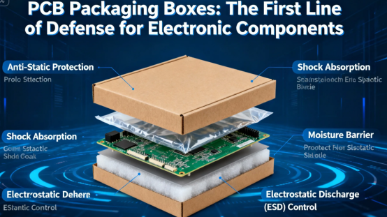
PCB packaging boxes are specially designed packaging solutions for printed circuit boards. Their primary function is to protect precision electronic components from physical damage, electrostatic discharge, dust contamination, and humid environmental conditions during transportation, storage, and usage.
A high-quality PCB packaging box not only requires a sturdy exterior but also typically includes specialized PCB mounting brackets and shock-absorbing materials to prevent the circuit board from shaking or colliding during transit.
In industrial applications, these boxes are often made of durable, high-strength materials such as polycarbonate, ABS, aluminum alloy, or cost-effective, recyclable cardboard. These materials offer dustproof, waterproof, and impact-resistant properties, ensuring long-term resilience and protection to meet the demands of various environments.
Static Shielding and Protection: Safeguarding Against ESD Risks
Electrostatic discharge (ESD) is one of the most significant threats to printed circuit boards and other sensitive electronic components during shipping and storage. Even a small static charge can cause irreversible damage to circuit boards, leading to costly failures and compromised performance. To combat this risk, PCB packaging incorporates static shielding and protection as a core element of its design.
Manufacturers rely on specialized packaging materials such as anti-static bags and anti-static foam shippers to create a protective barrier around PCBs. These materials are engineered to dissipate static charges and prevent them from coming into contact with the boards or their components. Static shielding not only protects the integrity of the electronic device but also ensures that the final product reaches its destination intact and fully functional.
Proper packaging techniques, including the use of static shielding materials, are essential for safeguarding PCBs against ESD during every stage of handling and transportation. By prioritizing ESD protection, companies can maintain the quality and reliability of their circuit boards, reduce the risk of costly returns, and uphold their reputation for delivering high-performance electronic components.
Cushioning and Padding: Enhancing Shock Absorption and Safety
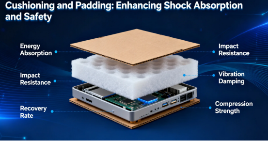
During shipping and handling, printed circuit boards are vulnerable to shocks, drops, and vibrations that can cause physical damage to both the board and its delicate components. To address these risks, effective PCB packaging solutions incorporate cushioning and padding as a fundamental layer of protection.
Materials such as bubble wrap, foam inserts, and custom padding are commonly used to create a shock-absorbing environment within the packaging. These packaging materials help to distribute impact forces, minimize movement, and prevent direct contact between the PCB and the outer box. By reducing the risk of shifting and collisions during transit, cushioning and padding play a vital role in maintaining the safety and integrity of the product.
Selecting the right combination of packaging materials and inserts allows manufacturers to create a tailored solution that meets the specific needs of each shipment. This attention to detail ensures that PCBs and their components are protected from shocks and arrive at their destination safely, ready for use or further assembly.
Packaging Methods: Techniques for Optimal PCB Security
Choosing the right packaging method is essential for ensuring that PCBs are shipped and handled with maximum security. A widely adopted approach combines static shielding with cushioning—using anti-static bags to protect against ESD and foam inserts or bubble wrap to absorb shocks. This dual-layer method addresses both electrical and physical hazards, providing comprehensive protection for circuit boards.
For shipments with unique requirements, custom packaging solutions may be developed. These can include molded plastic cases, wooden crates, or other specialized packaging materials designed to fit the exact dimensions and fragility of the PCBs. The goal is always to create a secure environment that prevents movement, absorbs shocks, and shields against potential hazards during transit.
By carefully selecting packaging materials and methods tailored to the specific needs of each shipment, manufacturers can ensure that their PCBs are shipped safely and arrive at their destination without damage. This commitment to proper packaging not only protects valuable components but also enhances customer satisfaction and trust.
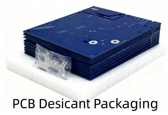
Packaging for Sensitive Components: Specialized Approaches
Certain electronic components, especially those used in industries like aerospace or medical devices, demand specialized packaging approaches due to their heightened sensitivity and strict requirements. These components may be susceptible to damage from moisture, temperature changes, or even minor physical impacts, making advanced protection essential.
To address these challenges, manufacturers use moisture-resistant packaging materials, such as vacuum-sealed bags or desiccant packs, to guard against humidity and condensation. Thermal insulation may also be incorporated to maintain stable temperatures during shipping. In addition, the packaging process itself is often adapted to ensure careful handling and minimize exposure to environmental risks.
By employing these specialized packaging materials and techniques, manufacturers can ensure that sensitive electronic components are fully protected throughout the shipping process. This attention to detail is critical for meeting industry standards, safeguarding the integrity of the components, and ensuring that they arrive at their destination in optimal working condition.
Detailed Overview of Three Types of PCB Packaging Boxes
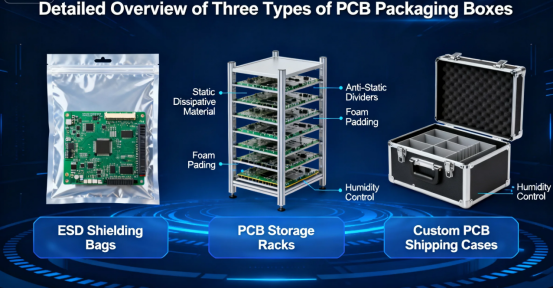
PCBMASTER Series: The Epitome of Professional Standards
The PCBMASTER series represents professional packaging solutions specifically designed for printed circuit boards. For example, Fibox’s CARDMASTER series of wall-mounted boxes, made from polycarbonate or ABS materials with superior strength, offer a protection rating of up to IP65, effectively preventing dust ingress and water spray damage.
These boxes feature precisely engineered internal structures, typically divided into two compartments—one for the circuit board and sensors, with slots for inserting the printed circuit board, and the other for terminals and wiring. This professional partitioned design makes PCBMASTER boxes ideal for instruments, measurement, monitoring, and process control equipment.
The PCBMASTER series usually comes in various sizes, ranging from the smallest 166×160×80 mm to the largest 390×316×167 mm, accommodating circuit boards of different dimensions. Their high-standard protective performance, superior strength, and professional internal layout make them the preferred choice in industrial environments.
Generic No-Logo Boxes: Economical and Practical Choice
Generic no-logo boxes are universal PCB packaging boxes without prominent brand identifiers. The greatest advantage of these boxes lies in their cost-effectiveness and wide applicability. They are a cost effective and economical solution for PCB packaging needs, making them ideal for short-term, one-way, or bulk shipments where affordability is important. For instance, SERPAC’s model 193C plastic box, measuring 9.5 inches long × 6.34 inches wide (approximately 241.30 mm × 161.04 mm), is made of polycarbonate with a gray transparent door design.
Key features of no-logo boxes include:
·Neutral appearance: Suitable for use by various companies without brand conflict concerns
·High cost-performance: Typically more affordable due to the absence of brand premiums
·Flexible application: Suitable for both product shipment packaging and workshop circulation
These boxes are widely used in electronics manufacturing, automotive, home appliance, and other industries, meeting general PCB packaging and protection needs. The absence of brand logos makes them particularly suitable as standardized packaging solutions within companies.
Customized Boxes: Perfect Solutions for Specific Requirements
Customized boxes are PCB packaging solutions specifically designed according to users’ unique requirements, perfectly accommodating circuit boards with special shapes, sizes, or protection needs. Everything from materials, colors, internal structures to exterior designs can be tailored to specific needs. A customized package can also include tailored labeling and pack options, such as orientation arrows, safety warnings, and detailed content identifiers, to meet specific shipping, protection, and branding requirements.
For example, some manufacturers offer aluminum alloy box customization services, allowing customers to select dimensions, lining materials, and load-bearing capacity as needed. Aluminum alloy boxes often use EVA shock-absorbing foam as lining material, with a load-bearing capacity of up to 80 kg, making them highly suitable for transporting precision or heavy electronic equipment.
Advantages of customized boxes include:
·Precise dimensional matching: Designed exactly according to PCB dimensions to prevent movement during transportation
·Functional expansion: Ability to add compartments, brackets, handles, and other convenient features
·Brand representation: Option to print company logos and identifiers to enhance professional image
·Specialized protection: Capability to incorporate anti-static, waterproof, shock-absorbing, and other specific characteristics
·Custom pack and labeling: The ability to customize the pack and labeling ensures that the package meets both protection and identification needs
For instance, Hongruida Industrial Co., Ltd. in Shenzhen offers plastic storage boxes that can be custom-made in various specifications and sizes, complete with lids, achieving dustproof and anti-static functionalities.
How to Choose the Right PCB Packaging Box: Key Considerations
Protection Level Requirements
Different application environments demand varying levels of protection for PCB packaging boxes. For example, Hoffman Enclosures’ model Q303013PCICC plastic box offers a protection rating of IP66, compliant with NEMA 4, 4X, 12, and 13 standards, making it suitable for more demanding industrial environments.
When shipping sensitive PCBs, it is crucial to select a durable container—such as a rigid box, foam shipper, or conductive case—to ensure electrical shielding, impact absorption, and physical protection during transit.
Selection considerations include:
·Dust and water resistance: Determine the required IP rating based on the usage environment
·Impact resistance: Consider potential physical impacts during transportation and use
·Corrosion resistance: Requirements for withstanding chemical corrosion in special environments
Material Characteristics
The material of PCB packaging boxes directly affects their protective performance and service life:
·Polycarbonate: Offers excellent impact resistance and transparency, suitable for applications requiring internal visibility
·ABS: Provides good rigidity and cost-effectiveness, representing an economical and practical choice
·Aluminum alloy: Delivers the highest structural strength and durability, ideal for heavy-duty equipment and harsh environments
After the fabrication of PCBs, selecting the appropriate packaging material is crucial to ensure protection and longevity.
Internal Structure Design
Professional PCB packaging boxes typically feature well-considered internal structures. For example, one patented design for PCB packaging and transportation boxes utilizes a base, multiple splicing frames, and a cover, connected by detachable connectors, achieving adjustable capacity based on PCB quantity.
Collaboration with assembly services can further optimize packaging design, ensuring that boxes are tailored for efficient assembly and shipping processes.
This design not only avoids waste of packaging materials but also prevents damage caused by shaking and collision due to excessive space inside the box.
Economic and Environmental Considerations
While meeting protection requirements, it’s also important to consider the economic and environmental aspects of packaging boxes. Packaging solutions should be tailored to meet the specific requirements and expectations of clients, ensuring that their needs for safety, quality, and brand presentation are addressed:
·Initial cost: Significant price variations among different materials and processes
·Service life: Number of reusable cycles—for example, SF Express’s “π-box” can be reused over 70 times
·Eco-friendly materials: Choosing recyclable materials such as polycarbonate and aluminum alloy
·Space efficiency: Features like tapered logistics boxes that reduce storage volume when empty
Development Trends and Innovations in PCB Packaging Boxes

Environmental Sustainability and Reusability
Eco-friendly and reusable designs have become important development directions for PCB packaging boxes. For instance, SF Express’s “π-box” reusable express box uses easily recyclable single-material PP honeycomb panels, with 96% of the entire box being recyclable. Protektive Pak is another example, offering recyclable, static-dissipative packaging solutions specifically designed for PCBs. This environmental concept is increasingly being applied to PCB packaging box designs.
Smart Features and Functional Integration
New-generation PCB packaging boxes are evolving toward smart functionality, including:
·Built-in sensors: Monitoring temperature, humidity, impact, and other data during transportation
·Adjustable internal structures: Such as adaptable PCB mounts for circuit boards of different sizes
·User-friendly opening mechanisms: Replacing traditional tapes with Velcro fastenings for convenient reuse
·Integration of proper labeling systems: Ensuring clear, accurate, and compliant markings for safe handling, correct orientation, regulatory compliance, and damage prevention during shipping
Lightweight and High-Strength Designs
Advances in material science have enabled lightweight designs without compromising strength. For example, tapered logistics boxes not only offer folding resistance, anti-aging properties, and high load-bearing capacity but also reduce storage volume when empty, improving logistics efficiency. Additionally, the development of lightweight and high-strength shipping boxes specifically designed for PCB protection ensures enhanced durability and static dissipation during transport.
Conclusion
As an indispensable component in the electronics manufacturing supply chain, PCB packaging boxes play a crucial role that cannot be overlooked. From standardized PCBMASTER boxes to economical and practical generic no-logo boxes, and fully customized solutions, companies can select the most suitable PCB packaging boxes based on their product characteristics, transportation environment, and brand requirements.
A well-designed PCB packaging box not only ensures products reach their destination safely but also enhances the company’s professional image, conveying value and trust to customers. In today’s rapidly evolving electronic technology landscape, choosing the right PCB packaging box provides comprehensive care for your high-precision circuit boards.
When shipping electronics and shipping components, best practices include using antistatic bags, antistatic foam, and antistatic shielding to protect sensitive devices and prototypes from electrostatic discharge and physical damage. Additionally, vacuum sealing and proper packing methods are essential to prevent moisture ingress and ensure safe transport of all electronic parts.
Author: Jack Wang