


Ultimate Guide to IC Packaging Substrates Manufacturing: HDI PCB & Fine Line Process
Introduction
1. Definition of IC
An IC (Integrated Circuit) is a miniature electronic device or component. Using specific manufacturing processes, all the necessary elements of a circuit—such as transistors, diodes, resistors, capacitors, and inductors—are interconnected and fabricated on a small piece or multiple pieces of semiconductor wafers or dielectric substrates, forming a compact structure that performs the desired circuit functions.
2. Packaging Forms
Packaging refers to connecting the circuit pins on the silicon die (IC) to external terminals using wires, allowing the IC to interface with other components. The term “packaging form” describes the type of housing used to mount the IC, such as lead frames or substrates.
3. IC Substrate Assembly and Structure
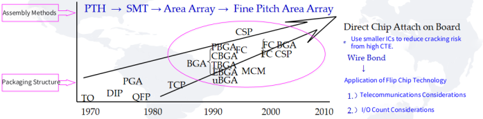
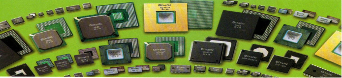
With the continuous advancement of single-chip IC packaging technology, new high-density IC packaging formats, such as BGA (Ball Grid Array) and CSP (Chip Scale Packaging), have emerged. This has led to the development of a critical new carrier for packaging—the IC packaging substrate.
IC packaging substrates belong to the HDI (High-Density Interconnect) product category and are among the fastest-growing high-end printed circuit boards today. They are widely used in modern communication devices and cutting-edge electronic products. At the same time, they differ significantly from traditional PCBs.
Overview of IC Packaging Substrates
1. Definition and Functions
Definition: An IC packaging substrate is a high-density printed circuit board used to package bare IC chips.
Functions:
Serves as the carrier for bare IC chips.
Contains internal circuitry to route signals between the bare chip and the PCB.
Provides multiple functionalities, including supporting, protecting, and securing the bare chip, conducting signals, facilitating heat dissipation, and enabling modular standards for components.
Related Terms:
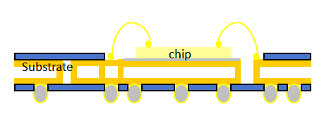
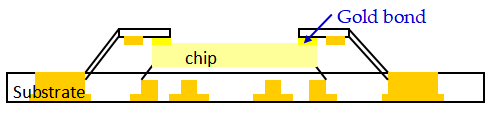
W/B (Wire Bonding): Wire bonding connection
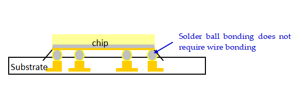
FC (Flip Chip Bonding): Flip-chip connection
TAB (Tape Automated Bonding): Tape-based automated bonding
BGA (Ball Grid Array): Ball grid array package
LGA (Land Grid Array): Land grid array package
CSP (Chip Scale Packaging): Chip scale package
2. Product Features
Ultra-thin core material with tight thickness tolerance: Board thickness ranges from 0.1 to 1.5 mm with a tolerance of ±30 µm.
Small and dense vias: Via diameters range from 30 to 100 µm, with hundreds to thousands of microvias per PCB.
Fine line width and spacing: 10–80 µm.
Small pads: Annular width of microvias is 50 µm.
Interconnection technologies: Buried, blind, and stacked vias.
Surface finishes: Ni/Au, soft gold, hard gold, Ni/Pd/Au, etc.
Compact unit size: ≤150 × 150 mm.
Dimensional tolerance: ±20–50 µm.
IC packaging substrates demand higher precision, high density, large pin counts, and compact size, with smaller vias, pads, and traces, and ultra-thin core layers. Therefore, they require advanced interlayer alignment, circuit imaging, plating, drilling, and surface treatment technologies. These requirements impose stringent standards on product reliability, equipment, materials, and overall production management.
3. Technical Challenges
Compared with traditional PCB manufacturing, IC packaging substrates face the following technical challenges:
Ultra-thin core processing control: Ultra-thin cores are prone to warping and dimensional changes. Breakthroughs are required in deformation control, lamination structures, panel shrinkage, lamination parameters, and interlayer alignment systems to effectively control core warping and final lamination thickness.
Microvia processing technology: Includes laser drilling of micro blind vias, mechanical drilling of micro through vias, via filling, and stacked via technology.
Ultra-fine line fabrication: Involves copper reduction, line compensation control, uniformity of plating, and uniform etching.
Interlayer alignment technology: Includes multi-lamination processes, LDI (Laser Direct Imaging) alignment exposure, and reference point positioning.
Solder mask processing: Includes via-filled solder mask for blind and through vias, solder mask alignment precision, and surface planarity control.
Surface finish technology: Includes electroplated soft gold, hard gold, and ENEPIG (electroless nickel/palladium/gold), with strict control over pad flatness and crystal grain uniformity.
Testing and inspection: Testing of tiny bonding pads requires high-precision AOI (Automated Optical Inspection) and micro-probe flying probe testers. A dedicated AOI repair workflow must be established to prevent quality issues caused by minor defects.
4. Types
4.1 Classification by Chip-to-Substrate Connection Technology
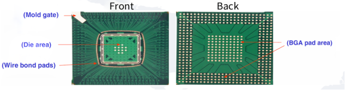
W/B Substrate (Wire Bond Substrate): Uses gold or aluminum wires for connection, typically bonded through thermocompression and ultrasonic processes.
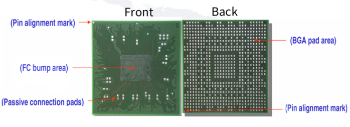
FC Substrate (Flip-Chip Substrate): Uses solder reflow and non-conductive adhesive curing for bonding.
TAB Substrate (Tape Automated Bonding Substrate): Uses gold-to-gold thermocomression bonding.
4.2 Classification by IC Packaging Type
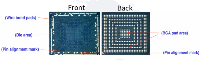
BGA Substrate (Ball Grid Array Substrate):
Definition: I/O terminals are arranged in an array of round or column-shaped solder balls beneath the package, providing the connection between the substrate and the PCB in a BGA configuration.
Advantages: Excellent thermal performance and electrical characteristics, supports a large number of chip pins, reduces signal transmission delay, and enables higher operating frequencies.
Material Types: Plastic, Tape, Ceramic, etc.
Type | PBGA | TBGA | CBGA | CCGA | Micro BGA | ||||||
Substrate | BT Resin (Bismaleimide-Triazine Resin) | Polyimide (PI) | Multilayer Ceramic | Multilayer Ceramic | Optional | ||||||
Encapsulation Structure | Over mold Glob Top Cap | Optional Cap | Optional Cap | Optional Cap | Over mold Glob Top Optional Cap | ||||||
Encapsulation Size | 7-50mm | 21-40mm | 18-32mm | 32-42.5mm | Chip Scale | ||||||
Die Orientation | Up / Down | Up | Up / Down | Up / Down | Up / Down | ||||||
Solder Ball | Solder Ball 63Sn / 37pb | Solder Ball 10Sn / 90pb | Solder Ball 10Sn / 90pb | Solder Column 10Sn / 90pb | Metal Ball Solder / Gold | ||||||
Pitch | 1.0/1.27/1.5 | 1.0/1.27/1.5 | 1.0/1.27/1.5 | 1.0/1.27/1.5 | 0.8/0.5 | ||||||
Area Efficiency(Chip=1) | 7.2 | 5.3 | 4.5 | 4.5 | 1-1.4 |
CSP Substrate (Chip Scale Packaging Substrate):
Definition: CSP refers to a variety of packaging forms where the IC package size is ≤1.2× (sometimes 1.5× or 2.0×) the size of the bare die. It is derived from existing packaging types and generally has a footprint equal to or slightly larger than the bare chip.
Included Types: Various Micro BGA, Mini BGA, FBGA, and similar small-scale packages fall under CSP.
Advantages: Meets the demand for increasing chip I/O pin counts, maintains a small ratio between chip area and package area, and significantly reduces signal transmission delay.
Type |
Rigid Substrate Interposer |
LeadframeType |
FLEX Circuit Interposer |
Transfer Molding (Process: Electroplate first, place solder balls, then perform sawing before final packaging.) |
wafer-level (Process: Packaging is fully performed at the wafer level, followed by sawing.) |


4.3 Mainstream Types of IC Packaging Substrates
PBGA Substrate (Wire Bond Plastic Ball Grid Array):
Wire bond plastic BGA substrates are widely used for packaging electronic components with medium to low I/O density, such as in computers and communication devices.
They can be classified into two main types: double-sided substrates and dual-sided HDI multilayer structures with 1–3 layers interconnected through laser-drilled micro blind vias (stacked via structures).
Reinforced glass-fabric-based buildup materials are typically used. The chip periphery is densely populated with bonding pads.
FCBGA Substrate (Flip Chip Ball Grid Array):
Flip-chip BGA substrates are widely used for high-speed computing and high I/O density electronic component packaging, such as in computers and communication devices.
Typically, both sides of the substrate contain 1–4 buildup layers interconnected through laser-drilled micro blind vias (stacked via HDI structures).
ABF (Ajinomoto Build-up Film) resin is the most commonly used buildup material. To ensure reliable interconnection between the chip bumps and the substrate, excellent surface flatness is required.
CSP Substrate (Chip Scale Packaging):
Chip scale packaging (CSP) substrates are widely used for electronic components with low I/O density, particularly in consumer and communication products that emphasize lightweight, thin, short, and compact designs.
They can be categorized into double-sided substrates and dual-sided HDI buildup structures with 1–2 layers interconnected through laser-drilled micro blind vias (stacked via structures).
Reinforced glass-fabric-based buildup materials are typically used. The chip periphery is densely populated with bonding pads, and the overall substrate thickness is generally less than 0.3 mm.
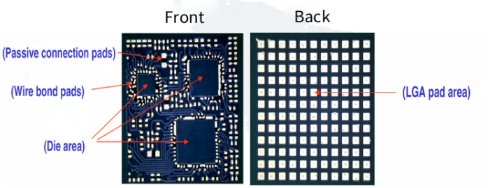
SiP, RF, and Camera Module Substrates (System-in-Package, Radio Frequency & Camera Module):
SiP, RF module, and camera module substrates are widely used in various portable communication and electronic devices.
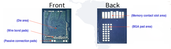
Memory Card Packaging Substrate:
Memory card substrates are widely used in a variety of electronic products such as computers, mobile phones, storage devices, and servers.
IC Packaging Substrate Manufacturing Process and Technical Features
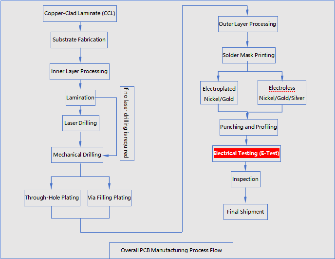
1. Process Flow
2. Substrate Fabrication Process
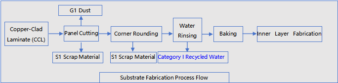
According to process requirements, the copper-clad laminate (CCL) is cut to the required dimensions. The four corners and edges of the substrate are then ground to create smooth edges. After grinding, the substrate is rinsed with water and dried.
Detailed Process:
1. Panel Cutting: Use a panel cutting machine to cut the copper-clad laminate (CCL) into the required dimensions.
2. Edge Grinding and Water Rinsing: Use a chamfering machine to round the four corners of the substrate into R-angles, and a deburring and cleaning machine to smooth all four edges.
The grinding process is wet, and the discharged wastewater contains a small amount of metallic copper.
3. Drying: Use a precision hot-air oven to dry the ground substrates before proceeding to the inner layer fabrication process.
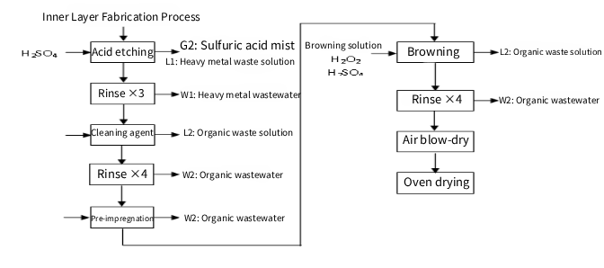
3. Inner Layer Fabrication Process
The inner layer fabrication mainly involves acid etching and other processes to form the circuitry of multilayer PCBs.
Detailed Process:
1. Degreasing: Remove grease and oils from the copper surface. Clean the copper using chemical cleaning agents, followed by three stages of counterflow rinsing.
2. Micro-Etching: The purpose of micro-etching is to create a slightly roughened, active copper surface for subsequent lamination, while removing residual oxides on the copper surface. The micro-etching depth is typically controlled at approximately 0.5–1.5 µm. Sulfuric acid and sodium persulfate (SPS) are used to etch the board and roughen the copper surface.
3. Acid Cleaning: Further remove oxides from the copper surface to ensure optimal adhesion.
4. Drying: Dry the rinsed boards using a precision hot-air oven before proceeding to the lamination step.
5. Photoresist Lamination: Apply a dry film composed of three layers: a polyester film, a photosensitive resist layer, and a polyethylene protective film.
6. Exposure: Using photomask imaging principles, expose the dry film to UV light to polymerize the photosensitive monomers, forming a pattern that is insoluble in mild alkaline solution.
7. DES Process (Develop, Etch, Strip):
Development: Dissolve the unpolymerized monomers in the dry film using 0.8–1.2% Na₂CO₃ alkaline solution.
Etching: Remove the unwanted copper with an acidic etching solution to form the desired circuit pattern.
Stripping: Remove the dry film from the substrate using 2–3% NaOH solution, completing the inner layer circuit formation.
4. Lamination Process Flow
Lamination is the process of stacking and pressing multiple double-sided boards to form a multilayer PCB.
The main steps in the lamination process are: pre-browning → lamination → post-treatment.
Detailed Lamination Process:
1. Acid Cleaning: Primarily removes copper surface oxides and foreign substances.
2. Degreasing and Cleaning: Mainly an alkaline wash to remove fingerprints, grease, and other oily residues from the copper surface.
3. Pre-Soak: Activates the copper surface to facilitate subsequent browning treatment.
4. Browning: Through a redox reaction, the copper surface is uniformly etched to roughen the board, increasing the contact area between the copper and the insulating substrate.
5. Post-Soak: Enhances the acid resistance of the browning layer.
6. Fusion: Semi-cured prepregs are cut to the required dimensions and placed on both sides of the browned inner layer boards, then secured together.
7. Stacking: Copper-clad laminates are placed over the prepregs, and according to the required number of layers, one or more inner layers and copper foils are stacked together.
8. Hot Lamination: The stacked multilayer boards are hot-pressed at 200–220°C under 2.45 MPa pressure for 2 hours.
9. Cold Lamination: During controlled cooling, residual stresses from the lamination process are released to prevent board warping.
10. Separation: Remove the backing kraft paper and mirror copper sheet to separate and obtain the multilayer substrate.
11. Drill Registration: Use a drill registration machine to locate the inner layer targets and drill positioning holes for forming and via processes.
12. Edge Routing: Remove excess semi-cured prepreg resin that has overflowed from the multilayer board edges during lamination.
13. Edge Grinding: Trim and smooth the edges of the cut multilayer substrate.
14. Mechanical Drilling: Cut aluminum plates or paper backing to the required dimensions, fix the multilayer board, and use drill shafts and drill bits to create through-holes or non-plated holes as needed.
5. Fine-Line Circuit Fabrication for IC Substrates
The methods for creating fine-line circuitry can be categorized as follows:
Subtractive Method: On a copper-clad board, use photochemical techniques, screen printing, or electroplated resist layers to transfer the pattern. The copper in non-pattern areas is then etched away.
Additive Method: Selective deposition of conductive metal onto the surface of an insulating substrate to form the desired conductive pattern.
Semi-Additive Process (SAP): Increase the thickness of the fine-line circuitry through patterned electroplating. The non-plated areas are rapidly etched in a differential etching process, leaving the plated portions to form the circuit.
Improved Semi-Additive Process: The line width and spacing of fine circuitry on IC substrates have evolved from 50 µm/50 µm to 25 µm/25 µm, and even down to 10 µm/10 µm, supporting ultra-fine “super-interconnect” technology.
5.1 Conventional Subtractive Method
The subtractive method is widely used in the manufacturing of HDI/BUM boards. However, the traditional subtractive method reaches its capability limit when producing multilayer boards with an average copper thickness of 20 µm and line width/spacing of 50 µm/50 µm, resulting in lower yields for finer lines.
To produce fine lines with line width/spacing below 50 µm/50 µm using the subtractive method while maintaining acceptable yields, it is necessary to:
Use low-profile copper foil (e.g., rolled copper),
Reduce the thickness of the copper laminate,
Ensure surface copper uniformity above 90%, and
Employ vacuum etching or other techniques to minimize undercut.
5.2 Ultra-Fine Line Semi-Additive Process (SAP)
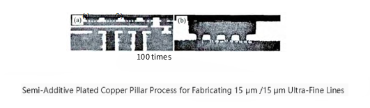
The semi-additive process (SAP) overcomes inherent limitations of both the subtractive and additive methods. Currently, domestic IC substrate fabrication can achieve line width/spacing as fine as 15 µm/15 µm.
The copper buildup in SAP can be achieved via DC plating or pulse plating. Pulse plating helps eliminate plating non-uniformity caused by solution polarization, refines the grain structure, improves copper purity, and reduces void formation.
Depending on how the microvias are formed, SAP can be categorized into:
Plated Copper Pillar Process
Direct Plated Fill Process
Ultra-Thin Copper (UTC) Process
5.2.1 Semi-Additive Process Types
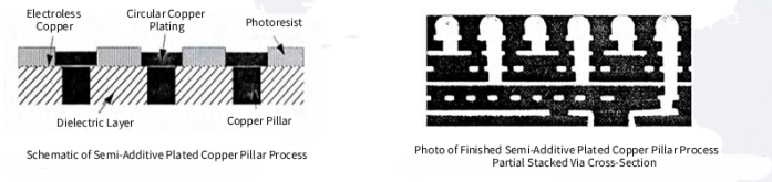
Plated Copper Pillar Process:
Advantages:
Interlayer connections use solid copper pillars, eliminating voids associated with plated fills.
Suitable for stacked via and pad-through-hole applications.
Capable of producing ultra-fine lines with a line width/spacing of 25 µm/25 µm.
Disadvantages:
Adhesion between the circuit lines and the dielectric layer is relatively weak.
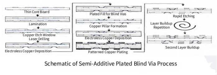
Semi-Additive Plated Fill Process for Blind Vias
Combines the advantages of the SAP process, laser drilling, and plated fill techniques.
The key factor lies in the formation method of the copper pillars.
Similarly, this process faces the issue of relatively weak adhesion between the circuit lines and the dielectric layer.
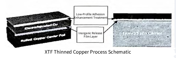
Ultra-Thin Copper (UTC) Process
The UTC process is expected to completely overcome the weak adhesion issues of fine-line circuits.
Utilizes a special copper foil structure to achieve an ultra-thin, smooth, low-profile base copper layer with excellent thickness uniformity.
The adhesion strength is significantly higher than that of conventional base copper produced via electroless deposition.
5.2.2 Semi-Additive Pattern Transfer Technology
The semi-additive pattern transfer process includes pre-treatment, dry film lamination, exposure, development, pattern copper plating, resist stripping, quick etching, and browning. Among these steps, exposure and quick etching are critical to the successful fabrication of ultra-fine circuits.
Key Equipment – High-End Direct Imaging Line Width/Spacing and Alignment Accuracy
Brand | Representative Model | Line Width/Spacing (µm) | Alignment Accuracy (µm) |
|---|---|---|---|
ORC | Extra 12 | 12 / 12 | 6 |
Ultra-Fine Line Exposure Technology
LDI (Laser Direct Imaging) technology provides high line width precision and excellent interlayer alignment.
Currently, high-end LDI equipment can achieve exposure line widths/spacings of 10 µm / 10 µm, with alignment accuracy of 5–10 µm.
Ultra-Fine Line Quick Etching Technology
Electroless copper layers may have crystalline defects, which can lead to undercuts during rapid etching.
Undercuts can be minimized by reducing the electroless copper layer thickness and using specialized etching solutions.
Using this approach, multilayer IC substrates with line widths/spacings of 15 µm / 15 µm have been successfully fabricated.
6. Summary of Process Technologies
The traditional subtractive method has inherent issues when producing ultra-fine lines, such as undercutting, uneven line widths, and insufficient line thickness. The semi-additive process (SAP) and its improved variants overcome many of these limitations of the subtractive method, but they still face challenges with line adhesion strength. In the future, ultra-thin copper with low profile and excellent thickness uniformity, combined with ALIVH technology, may become a new advanced semi-additive process. As IC packaging substrates continue to evolve toward higher-density wiring, the application of semi-additive processes is expected to expand further.
PCBMASTER IC Substrate Manufacturing Capabilities
IC Substrate Manufacturing Capabilities / Production Capacity | |||
Item | Specifications | ||
Material | Shengyi, BT, Mitsubishi, Doushan,Toshiba, LG, Ajinomoto Buildup Film (ABF) | ||
| MASS Production | Samples Production | |
Layer | 2-6 layer | 2-10 layer | |
Min Drilling | 100 µm | 100 µm | |
Bonding Finger | Min.Pitch | 105 µm | 95 µm |
Min.Width | 35 µm | 35 µm | |
Circuit Line | Min.Pitch | 95 µm | 25 µm |
Min.Width | 25 µm | 25 µm | |
Min.Spacing | 25 µm | 25 µm | |
Min.Weding ring | 80 µm | 80 µm | |
Min.Thickness | 2L | 100 µm | 100 µm |
4L | 300 µm | 200 µm | |
6L | 400 µm | 300 µm | |
10L | 800 µm | / | |
Line to PAD/EDGE | 100 µm | 100 µm | |
Soldermask | Solder PAD | 50 µm | 50 µm |
Solder DAM | 80 µm | 70 µm | |
Thickness | 20+/-5 µm | 20+/-5 µm | |
Flatness | 5 µm | 5 µm | |
Surface Finish | Hard Gold | Ni: 5-15 µm,Au: 0.2-0.5 µm | Ni: 5-15 µm,Au: 0.2-2 µm |
Soft Gold | Ni: 5-15 µm,Au: 0.3-0.8 µm | Ni: 5-15 µm,Au: 0.3-2 µm | |
ENEPIG-WB | Ni: 3-8 µm, Pd: 0.1-0.2 µm,Au: 0.1-0.2 µm | Ni: 3-8 µm, Pd: 0.1-0.2 µm,Au: 0. 1-2µm | |
ENEPIG-SMT | Ni: 3-8 µm, Pd: 0.05-0.15 µm,Au: 0.05-0.15 µm | Ni: 3-8 µm, Pd: 0.05-0.15 µm,Au: 0.05-2 µm | |
OSP | OSP: 0.1-0.3 µm | OSP: 0.1-0.3 µm | |

