


Essential Guide to HDI PCB Design and Manufacturing Best Practices
In the rapidly evolving field of electronic technology, electronic products are advancing rapidly towards miniaturization, high performance, and multifunctionality. From the smartphones and wearable devices we use daily to high-end fields like automotive electronics, medical equipment, and aerospace, the demands on electronic equipment are becoming increasingly stringent. Behind this, High-Density Interconnect (HDI) Printed Circuit Board (PCB) technology is quietly rising as the key force driving breakthroughs in electronic products.
HDI PCB OverviewHDI PCBs, or High-Density Interconnect Printed Circuit Boards, are most notably characterized by significantly higher wiring density compared to traditional PCBs. In contrast, a conventional board, or standard printed circuit board, has a lower wiring density and less advanced design approach, making it less suitable for compact, high-performance applications. In traditional PCBs, line spacing and trace width are typically around 150-250 micrometers (μm), whereas HDI PCBs allow line spacing and trace widths below 100 μm, and even finer levels with advanced manufacturing processes. This capability for fine-line routing enables electronic components to be integrated more densely onto the board, laying the foundation for the miniaturization and high performance of electronic products.
The emergence of HDI PCBs is not accidental; it was born out of the continuous development of electronic technology to meet market demands for higher-performing electronics. As chip technology advances, chip integration increases, and I/O pin counts rise, PCBs must provide more interconnection points and more efficient signal transmission paths. Simultaneously, consumer pursuit of portability drives PCBs to implement more functionality within limited space. Against this backdrop, HDI PCBs, with their unique advantages, have gradually become the mainstream choice in the electronic circuit field. One HDI board can often replace a few PCBs by integrating more functions and components into a single, compact design, reducing the need for multiple traditional printed circuit boards. HDI PCB technology enables miniaturization and high performance, supporting next-generation applications such as 5G, autonomous vehicles, and advanced medical devices.
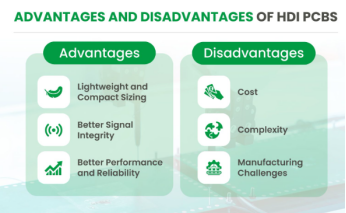
Technical Advantages of HDI PCBsSmaller Overall SizeHDI PCBs enable more circuit connections within a smaller space, allowing electronic products to be significantly reduced in size. Taking smartphones as an example, modern phones pack increasingly powerful features—high-performance processors, high-pixel cameras, large-capacity batteries, and various wireless communication modules—into compact devices. HDI PCBs achieve this tight integration through fine-line routing and micro-via technology, allowing phones to remain slim while continuously upgrading functionality. This advantage is equally evident in tablets, smartwatches, and other portable devices, offering consumers more convenient and compact user experiences.
Higher Component DensityThanks to finer traces and smaller vias, HDI PCBs can accommodate more electronic components within the same area. This not only improves board space utilization but also allows electronics to integrate more functional modules. For instance, in high-end wearables, HDI PCBs can house accelerometers, gyroscopes, heart rate sensors, Bluetooth modules, and various other sensors and communication components, enabling multifunctional integration. In automotive electronics, vehicle intelligence demands numerous sensors and control modules. The high component density of HDI PCBs allows complex functions to be implemented within limited space, providing strong support for technologies like autonomous driving and smart cockpits.
Shorter Routing DistancesThe high routing density of HDI PCBs results in shorter signal transmission paths. In high-speed signal transmission, signal delay is closely related to path length. Shorter routing effectively reduces signal transmission delay, increasing signal speed. For example, in 5G communication equipment operating at frequencies of several GHz or higher, signal speed and stability requirements are extreme. HDI PCBs meet these demands, ensuring fast and accurate data transmission. In high-performance computing, HDI PCBs similarly provide efficient signal transmission channels for CPUs, GPUs, and other high-speed chips, boosting overall system performance.
Lower Noise and CrosstalkSmaller line spacing and the use of thinner dielectric materials in HDI PCBs significantly reduce mutual interference (crosstalk) between signals. Additionally, shorter routing distances and better signal integrity help minimize noise generation. In medical devices like ECG and EEG machines, which detect extremely weak bioelectric signals, accuracy and noise immunity are paramount. The low noise and crosstalk characteristics of HDI PCBs ensure these devices accurately detect and process signals, providing reliable data for diagnosis. In aerospace, where electronics face complex electromagnetic environments, HDI PCBs’ excellent anti-interference performance ensures stable operation under harsh conditions.
Reduced Layer CountBy utilizing finer trace widths and spacing, HDI PCBs can achieve the same circuit functionality with fewer layers. Reducing layers lowers PCB manufacturing costs, reduces board weight, and improves reliability. In weight-critical applications like satellites and drones, the weight reduction from fewer layers is crucial. Furthermore, fewer layers mean fewer manufacturing steps, lowering the probability of quality issues and improving yield. HDI boards can also be more cost-effective than standard PCBs due to their reduced size and layer count, making them an attractive choice for many applications.
Key Technologies in HDI PCBsMicrovia TechnologyMicrovias, a core HDI technology, typically have diameters below 150 μm, even reaching tens of micrometers with advanced processes. They provide electrical connections between different board layers. Compared to traditional through-holes, microvias are smaller and denser, greatly enhancing routing efficiency. Laser drilling is currently the most common method. Lasers offer high energy density, precisely drilling tiny holes in the board’s insulating layer with minimal wall damage. Parameters like laser energy, pulse width, and drilling speed allow precise control over diameter, depth, and verticality. For example, in high-end smartphone PCBs, microvia diameters can be below 50 μm, significantly boosting routing density and signal transmission performance. The aspect ratio and aspect ratios of microvias are critical for reliability and manufacturability; maintaining a low aspect ratio (typically less than 1 or up to 2) ensures microvias are durable and can withstand thermal and mechanical stresses. Micro vias are essential for achieving high routing density and for connecting external pads directly to internal layers, enabling compact and reliable designs. After laser drilling, the plating process is crucial for ensuring reliable via connections, as it creates a conductive path and fills the vias to prevent voids and mechanical failures.
Thin-Core Dielectric MaterialsThin-core dielectric materials are crucial for HDI PCB performance. Located between conductive layers, they provide electrical insulation and support. Using thin-core dielectrics reduces board thickness and lowers signal transmission losses. These materials typically have low dielectric constant (Dk) and low dissipation factor (Df). Low Dk reduces signal delay and distortion, while low Df minimizes energy loss. Common materials include Polyimide (PI) and BT resin, offering good electrical properties, high mechanical strength, and heat resistance suitable for demanding HDI applications. For instance, in high-frequency communication equipment, low Dk/Df materials effectively reduce signal attenuation, improving communication quality. The use of multilayer PCB construction in HDI stackups is essential for achieving the high-density, multi-layered circuit boards required in advanced electronics.
Laser Drilling TechnologyAs mentioned, laser drilling is the primary method for microvia formation, playing a vital role in HDI manufacturing. Compared to mechanical drilling, it offers high precision for extremely small vias, high speed and efficiency, and non-contact processing that avoids mechanical damage, improving yield. Advanced laser drilling systems incorporate high-precision positioning and automated controls for precise hole placement, diameter, and depth. Optimizing parameters like laser energy, pulse width, and drilling speed enhances microvia quality and reliability. For example, state-of-the-art PCB factories achieve drilling speeds of thousands of microvias per minute, with diameter accuracy controlled within ±5 μm.
Fine-Line Circuitry TechnologyThis technology creates extremely fine traces and tiny pads on HDI PCBs for higher routing density and component integration. With advancing processes, trace width/spacing can now reach 3/3 mils (0.0762 mm) or less. Achieving this requires high-precision photolithography and etching. During photolithography, high-resolution equipment and photoresist precisely transfer circuit patterns onto the copper foil. Etching then removes unwanted copper to form the fine features. Strict control of parameters (exposure time, developer concentration, etch rate) and a clean environment are essential. For instance, in flagship smartphones, this technology enables complex layouts supporting high-performance operation. HDI design directly influences the lamination process and stack-up complexity, as designers must carefully plan the sequence and structure of layers to accommodate fine-line routing and advanced via types.
Thin Copper TechnologyThis involves using very thin copper foils, down to 1 oz (≈35 μm) or less. Thin copper enables finer traces and improves signal transmission performance. Manufacturing requires specialized processes and equipment to ensure foil quality and adhesion. Etching control becomes more critical to avoid over- or under-etching. Thin copper technology must synergize with other technologies like fine-line circuitry and microvias. For example, in ultra-high-speed circuits, thin copper reduces resistance and inductance, enhancing signal integrity.
Application Fields of HDI PCBsConsumer Electronics
Smartphones: The most widespread application. Integrating features like high-res cameras, 5G modules, powerful processors, and large batteries demands high space efficiency, signal performance, and thermal management. HDI PCBs meet these needs with fine routing, microvias, and excellent electrical properties. Flagship phones use multi-layer HDI PCBs with microvias and fine lines for high-speed data, efficient cooling, and slim designs. The use of advanced semiconductor packages in smartphones further enables miniaturization and high performance, supporting the integration of more features in smaller devices.
Tablets: Similarly require dense integration of displays, processors, memory, and wireless modules within thin profiles. HDI PCBs provide the density and electrical performance needed for powerful, feature-rich tablets. High-end models use 6-8 layer HDI for high-speed data transfer between processors and components, ensuring stability.
Wearables: Smartwatches and fitness trackers have extreme size/weight constraints while needing multiple functions (activity tracking, heart rate, sleep monitoring, Bluetooth). HDI PCBs are ideal due to small size, high integration, and low power. They enable tight integration of tiny sensors, processors, and Bluetooth modules for multifunctionality, miniaturization, stable signals, and low power consumption.
Automotive Electronics
Infotainment Systems: Increasingly complex systems (large displays, navigation, multimedia, Bluetooth) require efficient signal transmission and reliable connections. HDI PCBs ensure stable operation. Luxury cars use multi-layer HDI for high-speed data transfer between processors, displays, and audio chips, enabling smooth user experiences.
ADAS (Advanced Driver Assistance Systems): Systems like adaptive cruise control, automatic emergency braking, and lane departure warning demand ultra-fast sensor data processing and transmission. HDI PCBs meet the real-time and accuracy requirements. For example, in adaptive cruise control, HDI PCBs rapidly transmit radar/camera data to processors for precise vehicle speed/distance control.
EV Powertrains: Key components like Battery Management Systems (BMS) and motor controllers rely on HDI PCBs. They enable precise control/communication between battery modules and efficient power transfer between controllers and motors. In BMS, HDI PCBs accurately collect and transmit voltage, current, and temperature data from multiple cells to the main controller for safe and optimized battery usage.
Medical Devices
Portable Devices: Glucose meters, blood pressure monitors, digital stethoscopes need compact size, multifunctionality, signal accuracy, and reliability. HDI PCBs enable miniaturization and precision. For example, in glucose meters, HDI integrates sensors, processors, and displays for fast, accurate readings. The adoption of advanced semiconductor packages in medical devices is also crucial for enabling miniaturization and high performance, supporting the integration of complex functions in small, reliable devices.
Imaging Equipment: X-ray, CT scanners, MRI machines demand extremely high signal speed and precision. HDI PCBs provide the high-speed, stable transmission channels essential for accurate image data acquisition and processing. In CT scanners, HDI quickly transfers vast detector data to computers for high-quality image reconstruction.
Implantable Devices: Pacemakers, insulin pumps require extreme reliability and biocompatibility. HDI’s multilayer structure and fine-line technology allow complex functionality in tiny spaces, while stability ensures long-term operation in the body. For instance, pacemaker HDI PCBs integrate power management, signal processing, and pacing control within minimal space, reliably operating in complex physiological environments.
Aerospace
Avionics: Flight control, navigation, and communication systems demand minimal weight/size, high reliability, and EMI resistance. HDI PCBs are ideal. For example, flight control systems use HDI to densely connect sensors, controllers, and actuators for precise aircraft attitude control, reducing weight and improving fuel efficiency.
Satellite Electronics: Facing extreme temperature, radiation, and microgravity, satellite electronics require utmost reliability and stability. HDI PCBs provide high integration while ensuring long-term operation. For example, satellite communication systems use HDI for high-speed data transfer between modules, ensuring stable ground communication. Weight reduction also lowers launch costs.
Missile Guidance Systems: Demand extreme signal processing speed and accuracy within tight space constraints for processors, sensors, and communication modules. HDI PCBs meet real-time and precision needs. For instance, inertial navigation systems use HDI to rapidly transmit accelerometer/gyroscope data to processors for precise missile flight control and targeting accuracy.
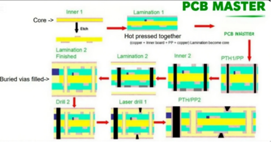
HDI PCB Manufacturing Process and ChallengesManufacturing Process
Fine-Line Fabrication: Requires high-precision photolithography and etching. Photoresist is applied to copper-clad laminate. Circuit patterns are exposed onto the resist using photolithography equipment. After development, the resist pattern acts as a mask. Etchant removes unprotected copper, forming fine traces. Precise control of exposure time, developer concentration, etch bath temperature, and etch time is critical for trace width, spacing, and edge quality. Increasing routing density is achieved by adding more layers to the PCB stack-up and utilizing advanced via techniques such as microvias, blind vias, and buried vias.
Microvia Fabrication: Primarily laser drilling. High-energy laser pulses melt or vaporize insulating material, forming microvias. Precise control of laser energy, pulse width, speed, and position ensures correct diameter, depth, and verticality. Post-drilling processes like desmear (removing debris) and electroless copper plating create a conductive via wall for interlayer connection. The plating process is essential for via reliability, ensuring that vias are properly filled and metallized to withstand thermal and mechanical stresses. Increasing routing density is also supported by the use of microvias and advanced multilayer stack-ups, allowing for more compact and complex circuit designs.
Lamination: Multi-layer HDI PCBs are bonded using the lamination process. Layers are pre-treated (cleaning, roughening) to improve adhesion. Layers are stacked according to design, separated by prepreg (PP) sheets acting as adhesive. Under high temperature and pressure, the prepreg melts, bonding the layers. Precise control of temperature, pressure, and time ensures uniform thickness, strong bonding, and avoids defects like voids or delamination. Sequential laminations are often used to build complex HDI stack-ups, enabling the integration of multiple layers and advanced via structures.
Surface Finishing: Applied to enhance solderability and corrosion resistance. Common finishes include… (Article cuts off here. Common finishes include ENIG, Immersion Tin, Immersion Silver, OSP, HASL etc.).
Introduction to HDI Printed Circuit Boards
HDI printed circuit boards (PCBs) represent a significant advancement in circuit board technology, utilizing high-density interconnect (HDI) techniques to achieve much higher wiring density per unit area than conventional circuit boards. By leveraging HDI technology, these boards can accommodate more intricate circuitry and a greater number of electrical connections within a smaller footprint, making them an ideal solution for today’s compact and high-performance electronic devices. Whether in portable video recording devices, handheld and mobile devices, or other space-constrained applications, HDI PCBs deliver superior electrical characteristics and higher connection pad density, enabling more complex and reliable interconnect solutions.
The increased routing density of HDI printed circuit boards allows for the integration of more components and advanced features without compromising quality or performance. This makes HDI PCBs a preferred choice across a wide range of industries, including consumer electronics, medical devices, and aerospace, where improved performance and miniaturization are essential. By maximizing wiring density per unit area, HDI printed circuits support the ongoing trend toward smaller, lighter, and more powerful products, all while ensuring reliable operation and excellent electrical performance.
HDI PCB Design Fundamentals
Designing HDI PCBs requires a deep understanding of advanced interconnect techniques and careful planning to achieve higher wiring density and optimal electrical performance. Key design fundamentals include the use of blind and buried vias, microvias, and via-in-pad methods, which allow for efficient vertical and horizontal routing within a limited unit area. These features enable designers to pack more components onto the board, supporting the integration of high-performance CPU and GPU chips and other advanced features.
The HDI PCB design process involves selecting the appropriate layer count and materials to balance performance, manufacturability, and cost. Designers must also consider the manufacturing process, as the use of fine lines and small vias demands precise fabrication techniques. Specialized PCB design software and simulation tools are essential for creating and validating complex layouts, ensuring that signal integrity and electrical performance are maintained throughout the board. By leveraging HDI technology, engineers can achieve higher density per unit area, enabling the development of sophisticated circuit boards that power the latest innovations in electronics.
HDI PCB Layout and Stack-ups
The layout and stack-up of an HDI PCB are crucial to its overall performance and reliability. Effective HDI PCB layout involves the strategic placement of components, traces, and vias to minimize signal interference and maximize routing density. By utilizing blind and buried vias, designers can create intricate interconnections between layers, allowing for more compact and efficient designs. This approach is especially important in devices like mobile phones and laptop computers, where space is at a premium and high density interconnection layers are required to support advanced features.
Stack-up design refers to the arrangement of the PCB’s layers, including the selection of dielectric materials, copper foils, and solder masks. Optimizing the stack-up is essential for achieving the desired electrical and thermal performance, as well as ensuring the board’s mechanical stability. Advanced stack-up configurations enable the creation of complex multilayer PCBs with high density interconnection layers, supporting the development of smaller, more powerful electronic devices. By carefully planning the PCB layout and stack-up, designers can deliver products that meet the demanding requirements of today’s high-performance applications.
Manufacturing HDI Circuit Boards
The manufacturing of HDI circuit boards involves a series of specialized processes and advanced technologies designed to achieve high connection pad density and superior electrical characteristics. Key steps include laser drilling for the creation of microvias, sequential lamination to build up multilayer structures, and copper filling to ensure reliable electrical connections. Each stage of the manufacturing process must be meticulously controlled, from material selection and layer creation to via formation and plating, to guarantee that the finished product meets stringent quality standards.
High-precision registration technologies are essential in HDI PCB manufacturing, as they enable the accurate alignment of multiple layers and the formation of complex high density interconnection layers. These technologies ensure that even the most intricate designs can be produced with exceptional accuracy and repeatability. By employing advanced manufacturing processes such as sequential lamination and copper filling, manufacturers can produce HDI PCBs with increased routing density and superior electrical performance, supporting the development of next-generation electronic devices.
Benefits of Using HDI PCBs
HDI PCBs offer a range of significant benefits that make them the preferred choice for modern electronic design. One of the primary advantages is improved performance, as the higher routing density and advanced interconnect features enable faster signal transmission and reduced power consumption. This allows for the creation of smaller, more powerful devices with advanced features such as high-speed processing and excellent mounting stability.
The use of HDI technology also enables a reduction in layer count, resulting in thinner finished board thickness and lower production costs without sacrificing functionality. HDI PCBs deliver superior electrical characteristics, including enhanced signal integrity and reduced interference, making them ideal for demanding applications in game consoles, personal computers, and medical devices. By leveraging the benefits of HDI PCBs—such as higher connection pad density, increased routing density, and improved electrical performance—designers and manufacturers can develop innovative products that meet the ever-increasing demands for miniaturization, speed, and reliability in today’s electronics market.
A.What is the difference between HDI PCBs and traditional PCBs?
Q. In terms of wiring density, traditional PCBs typically feature line spacing and trace widths of 150-250 μm, whereas HDI PCBs achieve values below 100 μm. Regarding vias, traditional PCBs use relatively large through-holes, while HDI PCBs employ microvias with diameters smaller than 150 μm. HDI PCBs enable higher component integration density, allowing complex functionality within smaller form factors. They are commonly used in space-constrained, high-performance applications like premium smartphones and avionics. Traditional PCBs are generally preferred for cost-sensitive, less demanding electronic devices with moderate performance requirements.
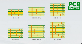
A.What types of HDI PCBs exist?
Q.
·Type I: Features single-layer microvias on one or both sides of the core layer. Interconnects use plated microvias and plated through-holes (PTHs), incorporating blind vias but no buried vias.
·Type II: Similarly employs single-layer microvias on one/both core sides with plated microvias and PTHs for interconnection, but includes both blind and buried vias.
·Type III: Contains at least two layers of microvias on one/both core sides, interconnected via plated microvias and PTHs, with both blind and buried vias.
HDI constructions are also defined using structural notations like "1 + n + 1", where "1 + n + 1" denotes a single microvia layer (analogous to Type I/II).
A. What are the key technologies for manufacturing HDI PCBs?
Q.
·Microvia Technology: Microvias (typically <150 μm diameter) enable critical interlayer connections, primarily fabricated via laser drilling to enhance routing efficiency.
·Thin-Core Dielectric Materials: Materials with low dielectric constant (Dk) and dissipation factor (Df) reduce board thickness and signal transmission loss.
·Laser Drilling Technology: High-precision, non-contact process for microvia creation, ensuring rapid production and consistent quality.
·Fine-Line Circuitry: Enables ultra-fine traces and micro-pads through high-accuracy photolithography and etching, boosting routing density and component integration.
·Thin Copper Technology: Utilizes thin copper foils (e.g., ≤1 oz) for refined traces and improved signal integrity, requiring stringent etching process control.
A. How to select the appropriate HDI PCB?
Q. Selection should prioritize application requirements:
·For size/performance-critical applications (e.g., smartphones), choose HDI PCBs with high routing density and optimized electrical performance.
·For thermal management needs (e.g., high-power modules), prioritize materials and structural designs with enhanced thermal conductivity.
Manufacturing capability and quality systems are critical—select suppliers with advanced processes and rigorous quality control to ensure compliance with specifications and standards.
Cost-effectiveness must be balanced with performance; evaluate solutions offering optimal technical benefits within budget constraints.
Why choose PCBMASTER: https://www.pcbmaster.com/why
Join us: https://www.pcbmaster.com/login

