


Understanding HDI-Buried and Blind Vias: Key Differences and Applications
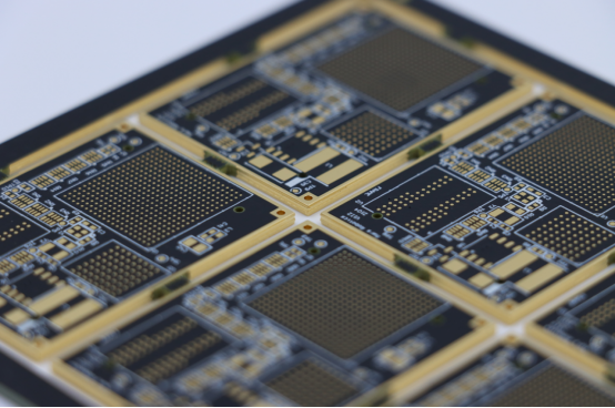
HDI vias, or High-Density Interconnector vias, are essential components in modern PCB (Printed Circuit Board) design. They are tiny electrical pathways used to connect different layers of a PCB, enabling more complex and compact circuit boards. As electronics become smaller and more powerful, HDI vias play a crucial role in meeting these demands by allowing for more interconnections in a limited space.
In PCB manufacturing, vias are vital for creating reliable electrical connections between the top and bottom layers of the board, and sometimes across multiple layers. HDI vias, specifically, offer the advantage of fitting more connections into smaller spaces, making them ideal for high-performance devices like smartphones, wearables, and medical equipment.
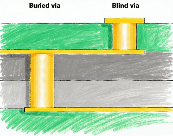
Buried and blind vias are two specialized types of HDI vias. Buried vias are fully contained within the inner layers of the PCB, while blind vias only connect the outer layer to one or more inner layers. Both types help improve the density, performance, and overall design flexibility of advanced PCBs, which are crucial for the next generation of electronic devices.
What Are HDI-Buried Vias and How Do They Function?
HDI-buried vias are small, conductive pathways embedded within the layers of a high-density interconnector (HDI) PCB. Unlike standard vias, which pass through the entire board, buried vias connect internal layers without reaching the outer surface. They are hidden inside the PCB structure and are typically used to create complex multi-layered designs. These vias are crucial in modern electronics because they allow for more efficient use of space, making devices smaller and more powerful.
Buried vias function by connecting two or more internal layers of the PCB without interrupting the surface. They play an essential role in high-density designs by enabling better use of limited space, ensuring electrical signals can pass between different layers without the need for visible connections. This leads to improved performance and more compact designs for devices like smartphones, tablets, and wearables.
To create buried vias, manufacturers drill small holes through the PCB layers and then fill these holes with conductive material, usually copper. This process is done without drilling through the outer layers of the board, making the vias "buried" within the inner layers. The vias are then connected electrically to the necessary circuits, creating an efficient path for signals.
Key Characteristics of Buried Vias
Buried vias are located entirely within the internal layers of a PCB, and they cannot be seen from the outer surface of the board. Their structure involves carefully drilled holes filled with conductive material that link internal layers, improving signal routing. Because they don't disrupt the outer layers, buried vias contribute to the smooth, uninterrupted surface of the PCB, essential for high-density, high-performance devices.
One of the major benefits of buried vias is their ability to minimize signal interference and crosstalk. By positioning vias inside the board rather than on the surface, they reduce the risk of electrical noise between components. This leads to better signal integrity, especially in designs where high-speed data transmission is critical, like in communication devices.
Additionally, buried vias increase PCB reliability and durability by keeping the surface of the board free of excess drilling. This ensures that the outer layers remain intact and better protected from mechanical stress and potential damage, ultimately contributing to a more robust and long-lasting product.
What Are Blind Vias and How Do They Differ from Buried Vias?
Blind vias are a type of via used in PCB design, which connects the outer layer of the board to one or more internal layers, but does not go all the way through the board. These vias are "blind" because they start from the outer layer and end at an internal layer without penetrating the entire thickness of the PCB. Blind vias are typically used in designs that require high density but want to avoid the added complexity and space usage of through-hole vias.
Unlike buried vias, which are entirely hidden within the internal layers, blind vias have a visible entry point on the outer surface. This makes them suitable for applications where access to certain layers from the exterior is needed, but where through-hole vias are not feasible. While buried vias are used to interconnect internal layers without affecting the outer surfaces, blind vias offer a more flexible solution for compact, multi-layer PCB designs.
Construction of Blind Vias
The construction of blind vias involves drilling small holes into the outer layers of the PCB and extending them to the internal layers that need to be connected. These vias do not pass all the way through the board but connect specific layers to improve routing for electrical signals. The process typically involves drilling, plating the hole with copper, and then connecting the vias to the necessary circuits.
Manufacturers must carefully control the depth and placement of the blind vias to ensure that they connect the correct internal layers without interfering with the external layers. This method is particularly useful for high-density designs, where space on the outer layers is limited, but internal layers still need to be electrically linked.
Key Advantages of Blind Vias
Blind vias offer several advantages that make them ideal for certain PCB designs. One of the main benefits is their ability to help reduce the overall size of the board. By connecting external layers to internal layers without drilling through the entire PCB, blind vias allow designers to maintain high functionality while minimizing the space required for the vias themselves.
Additionally, blind vias help to reduce signal loss, as they provide more direct paths between specific layers, minimizing the need for long, complicated routing paths. This is particularly important for high-speed electronic devices, where signal integrity is critical. As a result, blind vias contribute to the performance and reliability of the PCB, especially in devices that demand both compact design and high efficiency.
Key Characteristics of Blind Vias
Blind vias are typically located on the outer layers of a PCB and extend to one or more inner layers, but not through the entire thickness of the board. This makes them highly effective for designs that require multiple layers but need to minimize the space used on the outer layers. These vias are common in multi-layer PCB designs where space is at a premium, such as in mobile devices, medical equipment, and wearables.
By using blind vias, designers can create compact PCBs that still meet performance demands. This is particularly valuable when designing small, complex electronic devices where every millimeter counts. However, blind vias do come with limitations. They are generally more complex and expensive to manufacture than traditional through-hole vias because of the precision required to drill and plate them. Additionally, while they help save space on the outer layers, they may not offer the same routing flexibility as buried vias, especially when multiple internal layers need to be interconnected.
Despite these challenges, blind vias are a valuable tool for achieving high-density designs in applications where space, performance, and reliability are critical.
What Are the Key Differences Between HDI-Buried and Blind Vias?
When designing high-density PCBs, choosing the right type of via is crucial for performance and efficiency. HDI-buried and blind vias are two popular options, each with distinct advantages depending on the design requirements. In this section, we will explore the key differences between buried and blind vias, focusing on their location, functionality, cost, and manufacturing complexity. Understanding these differences will help you select the best option for your specific PCB needs.
Comparing Location and Construction
The primary difference between HDI-buried and blind vias lies in their location and how they are constructed within a PCB. Buried vias are completely enclosed within the internal layers of the board. These vias do not reach the outer layers, making them invisible from the board’s surface. To create buried vias, manufacturers drill holes through the inner layers, then fill these holes with conductive material, ensuring no disruptions to the outer layers.
In contrast, blind vias are drilled from the outer layer into one or more internal layers but do not pass through the entire PCB. These vias only extend partway into the PCB, connecting the outer layer to internal layers, but stopping before reaching the opposite outer surface. This allows for electrical connectivity between the external and internal layers without impacting the board’s thickness or surface.
Differences in Functionality
The functionality of buried and blind vias varies due to their placement in the PCB structure. Buried vias are ideal for high-density designs where internal layer connections are required but the surface must remain uninterrupted. They provide a cleaner and more efficient way to route signals internally, making them suitable for complex devices like smartphones or medical devices.
Blind vias, on the other hand, offer flexibility in designs where the outer layers need to remain relatively clear for components, but there’s still a need for connections between internal layers. While buried vias are perfect for minimizing external layer disruptions, blind vias are better when the designer needs external access to certain layers without using through-hole vias.
Cost and Complexity
Buried vias tend to be more expensive and complex to manufacture than blind vias. The process of creating buried vias requires more precise drilling, and the vias must be completely enclosed within the inner layers. This added complexity can increase manufacturing time and cost, making buried vias more suitable for high-end, high-density applications where space optimization and performance are key.
Blind vias are somewhat simpler to produce because they only require drilling into the outer layers, making them slightly less costly. However, the complexity comes from the need to ensure that the vias only connect the correct internal layers without reaching through the entire PCB. While blind vias are generally more affordable, they may require more careful design to avoid disrupting the board’s overall layout.
Comparison Table
| Feature | Buried Vias | Blind Vias |
| Location | Within the internal layers only | Extends from the outer layer to internal layers |
| Functionality | Used for internal layer connections without affecting external layers | Used for connecting external layers to internal layers while minimizing surface disruption |
| Manufacturing Cost | Higher due to complexity | Lower than buried vias, but still requires precision |
| Use Case | High-density designs with multiple internal layers | Designs needing minimal surface interruption, such as wearables or automotive electronics |
| Signal Integrity | Higher due to fully internal connections | Good, but less efficient than buried vias for routing |
Design Considerations for Choosing Between Buried and Blind Vias
When to Use Buried Vias in Designs That Require High-Density Interconnections
Buried vias are ideal when designing PCBs that need high-density interconnections but also require multiple internal layers. They allow for compact designs by ensuring that all the via connections are hidden within the internal layers, freeing up the external layers for other components. These vias are best suited for applications like smartphones, tablets, and other compact, high-performance electronics that require space optimization without compromising on functionality.
For example, in a multi-layer PCB used for a mobile phone, buried vias would allow the designer to connect internal layers without adding to the thickness or disrupting the external layer space needed for other components like chips or antennas.
The Best Scenarios for Using Blind Vias in Designs That Need Minimal Surface Disruption
Blind vias are most beneficial in situations where minimal disruption to the external layers is required, but internal layer connections are still necessary. They are perfect for applications where the outer surface of the board needs to remain largely intact for mounting components or achieving a clean design. This makes them suitable for use in PCBs for wearable devices, automotive electronics, or medical equipment where both internal connections and surface usability are important.
For instance, a wearable device like a smartwatch might use blind vias to connect external layers to internal circuits without compromising the space needed for the display or other components on the surface of the board.
What Are the Key Applications of HDI-Buried and Blind Vias in Modern PCB Designs?
HDI-buried and blind vias play a crucial role in the design of modern PCBs, particularly in industries where space optimization, performance, and reliability are key. These specialized vias are widely used in consumer electronics, automotive systems, aerospace, and medical devices, enabling compact, high-performance designs.
Applications in Consumer Electronics
HDI-buried and blind vias are essential in modern consumer electronics, particularly in smartphones, tablets, and wearables, where space is limited, and performance demands are high. These vias enable compact PCB designs that still support high-density interconnections, allowing for faster data transmission and more powerful components within smaller devices. Buried vias, by connecting internal layers without disrupting the outer surface, help save valuable space, leaving room for screens, batteries, and sensors. Blind vias, on the other hand, are used to link outer and internal layers while maintaining a clean, usable surface for mounting components. This allows for sleek, multi-layered devices with superior performance.
For example, in smartphones, buried vias are used to connect internal circuits, ensuring that the design remains slim and efficient without sacrificing performance. Similarly, wearables like smartwatches rely on blind vias to connect internal components while maintaining a smooth, uninterrupted outer surface for the display and sensors.
Use in Automotive and Aerospace
In industries like automotive and aerospace, reliability and space optimization are critical, and HDI vias, both buried and blind, play a crucial role in meeting these needs. In these mission-critical systems, where every component must perform flawlessly, buried and blind vias enable high-density interconnections in complex multi-layer PCBs. These vias help reduce the board's size while enhancing the signal integrity, which is vital for the safety and performance of applications such as navigation, sensor systems, and control modules.
For instance, in automotive electronics, HDI vias ensure that the electronic control units (ECUs) work efficiently despite the limited space available in vehicle systems. In aerospace, HDI vias contribute to high-performance PCBs used in flight control systems, where reliability and minimal signal loss are paramount.
Applications in Medical Devices
Medical devices require the highest standards of precision and reliability, and HDI-buried and blind vias help meet these needs in compact, high-performance designs. These vias allow for smaller, more reliable PCBs in devices such as pacemakers, diagnostic machines, and portable medical monitors. Buried vias offer the advantage of hidden interconnections between internal layers, maintaining a smooth external surface, which is essential for implantable devices or devices that require a high degree of miniaturization. Blind vias, on the other hand, provide access to internal layers without compromising the surface space, allowing for better routing of power and signals.
For example, in portable medical devices like glucose monitors, blind vias help connect circuits without taking up valuable space, allowing the device to be both compact and efficient. In more complex devices like MRI machines, buried vias are used to ensure that high-density circuit boards remain reliable and functional in the demanding medical environment.
Examples of Common Products Using HDI-Buried and Blind Vias
Real-world Examples of Electronics Using HDI-Buried and Blind Vias
Many modern electronic products rely on HDI-buried and blind vias for their advanced functionality and compact design. High-end mobile phones like the iPhone use buried vias to maximize internal connectivity while keeping the device slim and lightweight. These phones have multiple layers of circuitry with interconnections hidden within the board, made possible by buried vias. On the other hand, devices like smartwatches or fitness trackers often employ blind vias to maintain the smooth exterior while ensuring that internal components are properly connected.
In medical devices, such as pacemakers or hearing aids, both buried and blind vias are used to create small, efficient, and highly reliable PCBs. These devices often require space-saving techniques to house advanced electronics while ensuring the device is safe for long-term use inside the human body.
Case Studies Showcasing the Impact of Using Buried and Blind Vias
One example is the development of a smartphone, where buried vias help maximize the internal layers for processing power, reducing the overall size of the phone without compromising on functionality. This results in a slimmer, more powerful device with a long battery life and quick data processing capabilities.
In the aerospace industry, a specific case study involved the design of a flight control system where buried vias were used to connect multiple internal layers of a PCB in a way that allowed for high-speed communication between sensors. The result was a more compact, reliable, and efficient system capable of withstanding harsh conditions, ensuring the safety and reliability of the aircraft.
These examples show how buried and blind vias are used to meet the complex requirements of modern electronic designs, from performance to reliability, while maintaining compact size and functionality.
What Are the Manufacturing Challenges and Solutions for HDI-Buried and Blind Vias?
Manufacturing HDI-buried and blind vias involves complex processes that require precision and specialized techniques. These vias are crucial for creating high-density, high-performance PCBs, but they come with challenges such as drilling accuracy, cost, and material handling.
Manufacturing Techniques
The process of creating HDI vias, including buried and blind vias, involves several key techniques. One of the most common methods used is laser drilling, which is essential for creating precise, small vias within the PCB layers. Laser drilling allows manufacturers to create tiny holes that connect internal layers without compromising the board's integrity. Once the vias are drilled, via filling is used to coat the holes with a conductive material, typically copper, which enables electrical signals to pass between layers. After the vias are drilled and filled, the board undergoes a process called via plating, where the inner walls of the holes are coated with a thin layer of metal, ensuring proper conductivity.
For buried vias, the holes are drilled only through internal layers, while for blind vias, they extend from the outer layer into the inner layers but don’t go through the entire board. The precision required in both cases is vital for ensuring proper signal transmission and reliability in high-performance PCBs.
Challenges in Fabrication
Manufacturing HDI-buried and blind vias presents several challenges. One of the biggest hurdles is precision—the vias must be drilled with extreme accuracy to ensure proper functionality and avoid damaging surrounding components. This is especially difficult with smaller vias, which are typically used in high-density designs. Small errors in drilling depth or placement can lead to faulty connections or compromised signal integrity.
Another challenge is cost. HDI vias are more complex and require specialized equipment and materials, making them more expensive to produce than traditional vias. Additionally, the labor and time required for the intricate drilling and plating processes add to the overall cost. Manufacturers must balance these costs with the need for high-quality, high-performance PCBs, especially in industries like consumer electronics, aerospace, and medical devices, where reliability and precision are paramount.
Technological Advancements
Recent technological advancements have made the manufacturing of HDI vias more efficient and cost-effective. One significant development is the improvement in laser drilling techniques, which now allow for even finer and more precise vias. This advancement reduces the potential for errors and improves the overall quality of the vias. Additionally, automated via filling and plating processes have been optimized, reducing production time and costs.
Another innovation is the use of fine-pitch via technology, which enables the creation of smaller vias that can be used in denser designs. These technologies allow manufacturers to scale the production of HDI PCBs while maintaining the high quality and performance required in modern electronic devices. With these advancements, the process of producing HDI vias has become more accessible and efficient, making it easier for companies to meet the growing demand for high-performance PCBs.
Cost Considerations and ROI of Using HDI-Buried and Blind Vias
Breakdown of How the Cost of Manufacturing and Designing with Buried and Blind Vias Can Be Optimized for Greater ROI
The cost of manufacturing HDI-buried and blind vias can be high, but there are ways to optimize these costs for a better return on investment (ROI). One approach is to streamline the via design by reducing the number of vias required without compromising the functionality of the PCB. By designing PCBs that use fewer, strategically placed vias, manufacturers can lower production costs while still achieving the desired performance.
Additionally, automation in the drilling, via filling, and plating processes can help reduce labor costs and improve efficiency. Manufacturers can also reduce waste by optimizing the materials used, ensuring that the copper filling and plating are applied only where necessary, which lowers the cost of raw materials. By carefully managing these factors, companies can maximize the ROI of using HDI vias in their designs.
How to Balance Performance Improvements with Cost-Effectiveness
While HDI vias provide significant performance benefits, such as enhanced signal integrity and higher density, manufacturers must balance these improvements with the cost-effectiveness of their designs. In high-end devices where performance is critical, such as smartphones, medical devices, and aerospace systems, investing in HDI vias is often essential. However, in lower-end consumer electronics, manufacturers may opt for simpler vias, such as traditional through-hole vias, to keep costs down.
To balance performance with cost, engineers should consider the specific requirements of the device, such as size, signal integrity, and reliability. In cases where high density and performance are needed, the cost of HDI vias is justified by the performance gains they bring. However, in less demanding applications, a simpler design may be more cost-effective. By carefully evaluating the device’s needs, manufacturers can strike the right balance between cost and performance to ensure the most efficient and profitable design solution.
How Do HDI-Buried and Blind Vias Contribute to Signal Integrity and PCB Performance?
Signal Routing Efficiency
HDI-buried and blind vias significantly improve the efficiency of signal routing within a PCB. These vias allow for more compact and optimized designs by providing clear paths for electrical signals to travel between layers. Buried vias, hidden inside the board, ensure that connections between internal layers are made without occupying valuable surface space, enabling faster signal routing in high-density designs. Blind vias, by connecting the outer layers to internal ones, also contribute to efficient signal flow while minimizing external disruptions.
By reducing the need for long, convoluted routing paths, both buried and blind vias help decrease signal resistance and delay, improving the overall speed and reliability of the PCB. This is particularly beneficial in devices requiring high-speed performance, such as smartphones, gaming consoles, and computers.
Electromagnetic Interference (EMI) and Crosstalk Reduction
Reducing Electromagnetic Interference (EMI) and crosstalk is critical in high-speed PCBs to maintain signal integrity. Buried and blind vias help address these issues by minimizing the exposure of sensitive signal paths to external interference. Buried vias, being internal to the PCB, are naturally shielded from external sources of EMI. This reduces the chance of signals from adjacent vias or traces affecting each other, ensuring that high-speed signals travel with minimal disruption.
Blind vias also help by isolating different signal layers. Since they only connect to specific internal layers, they help organize and control the routing of signals, reducing the likelihood of unwanted signal interference or crosstalk. These vias contribute to the overall electromagnetic compatibility (EMC) of the device, which is crucial for maintaining the performance of high-frequency circuits and ensuring regulatory compliance.
Thermal Management
Another important aspect of PCB performance is thermal management, especially in high-performance devices where components generate significant heat. HDI-buried and blind vias play a role in dissipating heat more effectively within the PCB. Since vias are conductive, they help spread the heat generated by the internal components throughout the board. Buried vias, which are embedded within the layers, contribute to better thermal distribution, helping prevent hot spots that could lead to component failure.
Blind vias also assist with heat dissipation by connecting the outer layers to the inner layers, which can then distribute the heat away from critical components. In designs where compactness and performance are paramount, such as in gaming consoles or medical devices, these vias help maintain the longevity and reliability of the device by ensuring that it operates at a stable temperature.
Factors to Consider in Enhancing PCB Performance with HDI Vias
The Importance of Precise Via Design and Placement
To ensure optimal performance in complex PCBs, precise via design and placement are essential. Both buried and blind vias must be carefully positioned to minimize signal loss, crosstalk, and thermal build-up. Incorrect placement can lead to inefficiencies in signal routing and compromised signal integrity, particularly in high-density designs. In advanced applications such as mobile phones or automotive systems, where precision is crucial, careful consideration must be given to how vias interact with the surrounding components and circuitry.
By using advanced simulation tools and design software, engineers can optimize the placement of vias to ensure that signals flow smoothly, heat is effectively managed, and space is used efficiently. This level of precision helps to maximize the performance and reliability of the PCB, especially in high-performance devices.
Best Practices for Ensuring Signal Integrity and Reduced Noise in High-Density Designs
Ensuring signal integrity and minimizing noise are top priorities in high-density PCB designs. To achieve this, several best practices can be followed. First, via size and placement should be optimized to avoid excessive resistance or capacitance that could affect the signal. Minimizing the length of signal traces and using proper ground planes around vias also helps to reduce noise and ensure cleaner signals.
For high-frequency applications, engineers often use differential pair routing with closely placed vias to improve signal quality. Via-in-pad designs and blind vias can help reduce noise by isolating sensitive signals from adjacent layers. Additionally, using low-inductance vias and choosing the right materials for plating and filling can reduce signal degradation, ensuring optimal performance in complex, high-speed systems.
By following these best practices, designers can enhance the signal integrity and overall performance of PCBs, ensuring that devices operate at their peak efficiency without interference or loss.
Conclusion
Understanding the differences and applications of HDI-buried and blind vias is crucial for designing high-performance PCBs. These vias help optimize signal routing, reduce electromagnetic interference, and improve thermal management, all of which contribute to the reliability and efficiency of modern electronic devices. By selecting the right type of via based on specific application needs, engineers and designers can ensure their PCBs meet performance goals while also being cost-effective.
As the demand for high-density interconnection (HDI) technology grows, finding a reliable PCB manufacturer becomes even more important. This is where companies like PCBMASTER come in. With years of expertise in the PCB industry, PCBMASTER specializes in producing high-quality PCBs that integrate advanced HDI-buried and blind vias. Whether you're designing for consumer electronics, medical devices, or aerospace, PCBMASTER can help deliver custom solutions tailored to your specific requirements. Let us support your designs with the precision and performance they deserve.
FAQs
What is the main difference between HDI-buried vias and blind vias?
Buried vias and blind vias differ mainly in their construction, placement, and usage within a PCB.
l Buried vias: These are completely contained within the inner layers of the PCB and do not appear on the outer surfaces. They are typically used to connect multiple internal layers of the board without disrupting the outer layers. Buried vias are ideal for high-density interconnection (HDI) designs where space optimization is critical, as they don't occupy valuable surface area.
l Blind vias: These connect an outer layer to one or more internal layers, but they do not pass all the way through the entire board. They have one end at the surface layer and the other at an inner layer, without reaching the opposite surface. Blind vias are used when you need to access the internal layers while maintaining a clean, unbroken external surface for other components or features.
In terms of usage, buried vias are better suited for internal layer connections in complex, high-density PCBs, while blind vias are preferred when external access to the internal layers is necessary without compromising the outer layer space.
Are buried and blind vias cost-effective for consumer electronics?
Buried and blind vias can be cost-effective for consumer electronics, but their cost-effectiveness depends on the design complexity and the performance needs of the device.
l Buried vias: While they require more precision and specialized equipment to manufacture, they are more beneficial for high-performance, compact designs. In consumer electronics such as smartphones, tablets, and wearables, where space is limited, the cost of buried vias is justified by the space savings and the high-density interconnections they provide. However, their manufacturing cost is higher due to the need for more layers and precise drilling.
l Blind vias: Generally less expensive than buried vias, blind vias offer a balance between cost and performance. They allow designers to use the external layers efficiently while still connecting the internal layers. Blind vias are commonly used in mid-tier electronics where a balance of cost and performance is required. They can be more affordable for applications where extreme miniaturization isn’t as critical but still need multi-layer connections.
For high-end devices, the performance benefits of both buried and blind vias often outweigh the added costs, particularly in devices requiring high-speed data transmission and compact designs.
What types of PCB designs benefit most from using HDI-buried and blind vias?
HDI-buried and blind vias are most beneficial in high-performance, high-density PCB designs where space optimization and signal integrity are critical. Here are a few specific scenarios:
l Smartphones and Tablets: These devices require compact designs with efficient internal routing. Buried vias are used to connect multiple internal layers without occupying the outer surface, freeing up space for displays, batteries, and antennas. Blind vias are used to connect internal layers while keeping the external surface intact for components like touchscreens and cameras.
l Wearables: Similar to smartphones, wearables like smartwatches require small, high-performance PCBs. Buried vias help maximize internal connectivity, while blind vias allow for external access to key layers without disrupting the design’s compactness.
l Automotive Electronics: In systems like engine control units (ECUs), buried vias are often used to ensure reliability and high-density interconnections without increasing the board’s thickness or space. Blind vias are also employed to facilitate high-speed communication while keeping the board surface clean and available for other components.
l Medical Devices: Devices such as portable glucose monitors or hearing aids benefit from HDI vias as they allow for miniaturization and improved functionality. Buried vias are used to maintain a compact and reliable connection between internal components, while blind vias provide easy routing to external layers.
How do HDI-buried and blind vias affect signal integrity in complex PCBs?
HDI-buried and blind vias enhance signal integrity in high-density PCBs by providing efficient routing paths while minimizing interference and signal loss. Here's how they contribute:
l Signal Routing: Buried vias help maintain a cleaner signal path by connecting multiple internal layers without disturbing the surface layer. Since they’re internal, they help avoid the added complexity of routing through external layers, which can cause signal delays and resistance. Similarly, blind vias provide direct, clear connections between external and internal layers, improving signal clarity by reducing the path length.
l Reducing Crosstalk and EMI: Both buried and blind vias contribute to minimizing crosstalk (interference from adjacent signal lines) and electromagnetic interference (EMI). Since buried vias are placed between layers, they’re shielded from external noise, making them ideal for high-speed and high-frequency applications. Blind vias, by isolating signals within a compact board layout, help reduce unwanted signal coupling between layers.
l High-Speed Data Transmission: By reducing via inductance and maintaining consistent trace impedance, both types of vias help ensure high-speed signal integrity, which is crucial in modern devices like 5G-enabled smartphones or gaming consoles.
What are the environmental considerations when designing with HDI vias?
When designing PCBs with HDI vias, there are several environmental considerations to keep in mind, particularly related to sustainability and the materials used:
l Material Selection: The materials used in HDI via manufacturing, including copper for via filling and laminates for PCB layers, should be eco-friendly and sourced from responsible suppliers. The increasing demand for sustainable products has led to the use of lead-free and halogen-free PCB materials, which are better for the environment compared to traditional materials.
l Manufacturing Waste: The drilling and plating processes for HDI vias, especially laser drilling, produce waste materials that should be handled responsibly. Manufacturers are increasingly adopting closed-loop systems to recycle materials like copper and reduce waste generated during production.
l Energy Efficiency: The advanced technologies used in HDI via manufacturing, such as laser drilling and automated plating systems, can be energy-intensive. Choosing suppliers who prioritize energy-efficient practices and renewable energy sources can help reduce the overall carbon footprint of PCB production.
l End-of-Life Disposal: As PCBs reach the end of their life cycle, ensuring that they are properly recycled and that hazardous materials are safely disposed of is crucial. Many manufacturers are adopting practices aligned with RoHS (Restriction of Hazardous Substances) standards to limit harmful chemicals in their products, further minimizing environmental impact.
By considering these environmental factors, manufacturers can reduce the ecological footprint of HDI via production and contribute to more sustainable electronics manufacturing.
Author Bio
Hi, I'm Carol, the Overseas Marketing Manager at PCBMASTER, where I focus on expanding international markets and researching PCB and PCBA solutions. Since 2020, I've been deeply involved in helping our company collaborate with global clients, addressing their technical and production needs in the PCB and PCBA sectors. Over these years, I've gained extensive experience and developed a deeper understanding of industry trends, challenges, and technological innovations.
Outside of work, I'm passionate about writing and enjoy sharing industry insights, market developments, and practical tips through my blog. I hope my posts can help you better understand the PCB and PCBA industries and maybe even offer some valuable takeaways. Of course, if you have any thoughts or questions, feel free to leave a comment below—I'd love to hear from you and discuss further!

