


What is mSAP? A Guide to the Modified Semi-Additive Process in PCB Manufacturing
As the demand for smaller, faster, and more powerful electronic devices grows, the need for advanced PCB manufacturing techniques becomes increasingly critical. mSAP (Modified Semi-Additive Process) has emerged as a revolutionary solution, offering unparalleled precision and efficiency in creating ultra-fine circuits. Unlike traditional methods, mSAP overcomes the limitations of conventional etching, enabling the production of high-density, high-performance circuit boards that meet the rigorous demands of modern electronics. This innovative process is shaping the future of PCB design, making it an essential tool for next-generation devices.
What is mSAP (Modified Semi-Additive Process)?
mSAP Definition and Background
mSAP, or Modified Semi-Additive Process, is an advanced method used in PCB (Printed Circuit Board) manufacturing. It is an improvement on traditional processes, particularly in creating high-precision circuits. In simple terms, mSAP allows manufacturers to add copper to the PCB in a controlled way, making it possible to create very fine lines and small spaces that are required in modern electronic devices.
The development of mSAP was driven by the limitations of older processes, such as traditional etching. In traditional methods, copper is removed from the board to form circuits, which can lead to inaccuracies when making very fine details. With mSAP, copper is added instead of subtracted, which improves the precision and allows for tighter line widths and smaller distances between components.
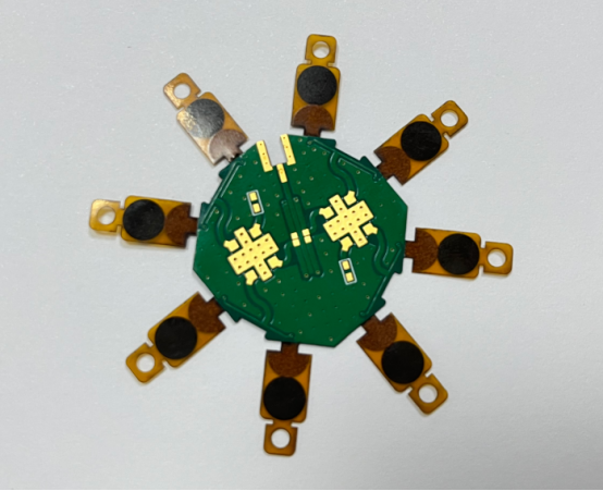
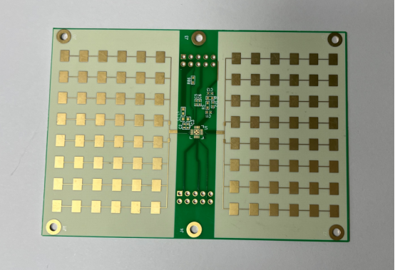
This process has become widely used in industries that require high-density interconnect (HDI) boards and chip packaging substrates, especially in the production of high-performance devices like smartphones, laptops, and 5G communication equipment. mSAP enables manufacturers to meet the increasing demand for smaller, faster, and more reliable electronics.
Key Advantages of mSAP
High Precision Circuits
One of the biggest advantages of mSAP is its ability to produce circuits with extreme precision. Traditional etching methods tend to create circuit lines with sloped sides, which can lead to weak points and reduce the overall quality of the PCB. In contrast, mSAP creates almost perfectly vertical walls for the copper traces. This means that the lines are more accurate, and the PCB can handle smaller components and higher frequencies without degradation.
For example, when manufacturing PCBs for smartphones or high-speed servers, where the circuits need to be extremely fine and precise, mSAP is the preferred method. The ability to produce sharp, vertical copper walls ensures that the signal integrity is maintained, even at tiny sizes.
Higher Wiring Density
mSAP is particularly useful in creating high-density circuits, meaning more circuits can fit into a smaller area. As electronics become more compact, there is a greater need to maximize the use of space on a PCB. mSAP allows manufacturers to pack more circuitry into the same footprint, supporting the trend toward smaller devices with more complex functions.
For instance, in advanced HDI (High-Density Interconnect) boards used in mobile phones, mSAP enables the integration of more layers and finer traces without compromising performance. This makes it possible to produce smaller, thinner, and more feature-packed devices.
Material Saving
Compared to traditional etching methods, mSAP is much more efficient in its use of materials. Traditional etching often involves significant waste of copper, as large areas of copper are removed to form the desired circuit pattern. This can result in a high percentage of the raw material being discarded, which is inefficient and costly.
mSAP, on the other hand, reduces material waste by adding copper only where it is needed. This "additive" approach saves copper and other materials, lowering production costs and reducing the environmental impact of manufacturing. In industries where cost-efficiency and sustainability are important, such as in the production of consumer electronics, this material-saving feature is a significant advantage.
By using mSAP, manufacturers can produce PCBs with much less copper waste, making the process more cost-effective and environmentally friendly.
How Does the mSAP Process Work?
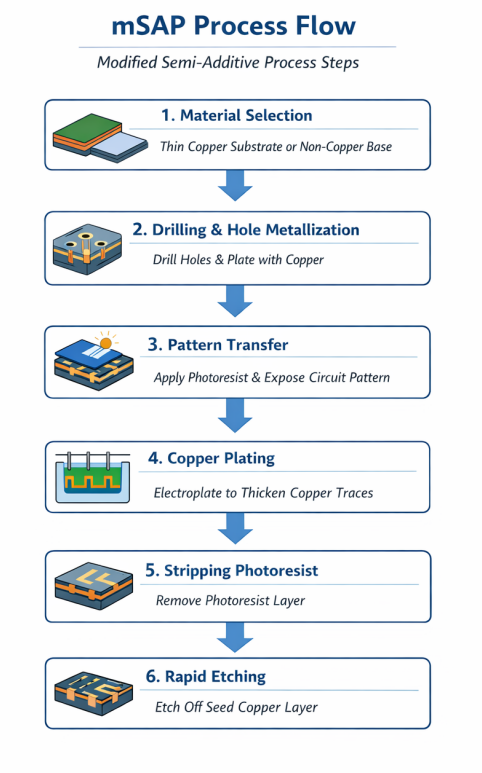
1. Selection of Starting Materials
The selection of starting materials is a critical first step in the mSAP process. Typically, a thin copper-clad substrate or a non-copper-insulated substrate is used. The choice of material plays a crucial role in ensuring the high precision and efficiency of the mSAP process.
Thin Copper-Clad Substrates: In mSAP, a very thin copper layer, often less than 3 microns, is used as the starting point. This thin copper layer is much thinner than what is used in traditional methods. The advantage of this thin layer is that it allows for more controlled and precise copper plating during the next steps of the process. It also helps avoid the material waste that typically occurs with traditional etching techniques, which often remove large amounts of copper.
Non-Copper Insulated Substrates: In some cases, the substrate may have no copper layer at all. This is common in processes that require the addition of copper only where needed. This method is used in specialized applications, such as flexible PCBs or multi-layered circuit boards.
Difference from Traditional Copper-Clad Boards: Traditional PCBs often use copper-clad laminates, where copper is initially thicker and later etched away to form the circuit. However, mSAP uses an additive approach, where copper is added only to areas needed for the circuit. This results in more precise circuit creation and significantly less copper waste, which is environmentally friendly and cost-effective.
In summary, the choice of starting material is crucial for ensuring the precise, efficient, and high-quality production of PCBs in the mSAP process.
2. Drilling and Hole Metallization
The second step in the mSAP process is drilling and hole metallization, which is essential for forming the conductive vias or holes in the PCB.
Drilling: Drilling creates the necessary holes for interconnecting different layers of the PCB. These holes are typically used to create vias, which allow electrical signals to pass between different layers of the board. The drilling process is done with precision, ensuring that the holes are the correct size and aligned with the design.
Chemical Copper Plating (Hole Metallization): After drilling, a chemical copper plating process is used to coat the interior of the holes with copper. This step is crucial for ensuring that the drilled holes are electrically conductive, allowing for effective connections between the layers of the PCB.
Importance in Multi-Layer Designs: In multi-layer PCBs, which are common in modern electronic devices like smartphones and computers, the reliability and strength of these vias are critical. The metallization step ensures that these vias are strong and electrically stable, which is essential for the performance and durability of the final product.
By using precise drilling and metallization techniques, mSAP guarantees that multi-layer PCBs have reliable connections, ensuring optimal electrical performance.
3. Pattern Transfer and Photoresist Film Formation
The third step in the mSAP process involves transferring the circuit pattern onto the PCB surface. This is done using a process called photolithography.
Photolithography: In this step, a light-sensitive photoresist film is applied to the PCB surface. The photoresist film is then exposed to ultraviolet (UV) light through a mask that contains the desired circuit pattern. The areas of the photoresist exposed to light become hard, while the unexposed areas remain soft and can be washed away.
Reversed Image Pattern: The photoresist creates a reversed pattern where the areas that should remain copper are exposed, and the areas that should be removed are covered by the photoresist. This step defines the outline of the copper traces that will be formed in the following stages.
Accuracy of Lithography: The photolithography process requires very high precision. Any slight misalignment or imperfection can result in defects in the final circuit, which can affect the performance of the electronic device. Therefore, the precision of this process is critical for ensuring the final product meets the required specifications.
Through photolithography, mSAP ensures that the exact copper traces needed for the circuit are defined and prepared for the next step of the process.
4. Circuit Thickening: Copper Plating
Once the circuit pattern is defined, the next step is to thicken the copper traces using copper electroplating.
Copper Plating: Electroplating is used to add copper onto the exposed areas of the substrate where the photoresist has been removed. This is done by immersing the PCB into a bath containing a copper solution and applying an electrical current. The copper ions in the solution are reduced and deposited onto the exposed areas of the PCB, thickening the copper traces to the required dimensions.
Achieving Desired Trace Thickness: The copper plating process allows manufacturers to control the thickness of the copper traces precisely. This is crucial because the thickness of the copper affects the electrical performance of the PCB. Thicker copper traces can handle higher currents, which is important for high-power applications.
Solving Uneven Copper Layers: Unlike traditional etching methods that can result in uneven copper layers, the electroplating process in mSAP ensures that the copper is deposited uniformly. This allows for more precise and consistent circuit traces, ensuring that the final PCB has a high-quality finish and reliable performance.
Copper electroplating plays a key role in creating thick, precise circuit traces that are essential for high-density, high-performance PCBs.
5. Stripping and Removing Photoresist
After the copper plating is complete, the next step is to remove the remaining photoresist to reveal the final copper traces.
Stripping Process: The photoresist is removed using a chemical solution that dissolves the resist, leaving behind only the copper traces. This step is important for cleaning the PCB and ensuring that no remnants of photoresist remain that could interfere with the next steps in the process.
Ensuring Clarity and Accuracy: By carefully removing the photoresist, mSAP ensures that the final circuit pattern is clear and accurate. Any leftover resist could result in poor electrical connections or manufacturing defects.
This step is essential for ensuring the PCB has clean, well-defined copper traces that will function properly in the final electronic device.
6. Rapid Etching: Removing the Seed Copper Layer
The final step in the mSAP process is rapid etching, which removes the thin seed copper layer that was initially deposited during the process.
Rapid Etching Process: In this step, a rapid etching solution is used to remove the thin seed copper layer that remains on the PCB, leaving only the thickened copper traces that were added during electroplating. The key to this step is that it only etches away the seed layer, without damaging the thicker copper traces.
Difference from Traditional Etching: Traditional etching methods remove large areas of copper from the entire surface, which can lead to uneven copper distribution. In contrast, rapid etching in mSAP is highly controlled and targets only the areas where the seed copper is present. This ensures that the final PCB has uniform copper traces, without the risk of damaging the main copper lines.
Protecting the Copper Traces: Rapid etching ensures that the final copper traces are not compromised, maintaining the quality and performance of the PCB. This is particularly important for high-density and high-precision applications, where even small defects can cause performance issues.
By using rapid etching, mSAP ensures that the final PCB has a high-quality, uniform copper trace with no leftover material that could affect performance.
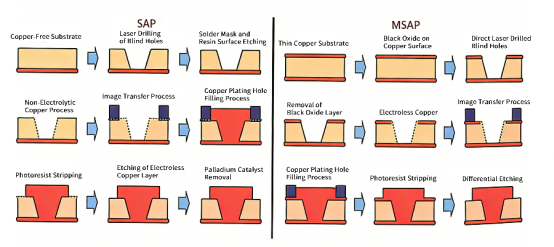
What is the Difference Between mSAP and Traditional Etching Methods?
Limitations of Traditional Etching Methods
What are the limitations of traditional etching?
Traditional etching methods, also known as subtractive processes, involve removing excess copper from a copper-clad substrate to form the circuit pattern. However, this method has several limitations, particularly when it comes to precision and the ability to produce fine, intricate traces.
Side-Etching and Precision Issues
One of the biggest issues with traditional etching is side-etching. When copper is removed, it does not always result in perfectly straight lines. The copper on the sides of the circuit traces can be etched away at an angle, causing the traces to become tapered or sloped rather than remaining straight and vertical. This phenomenon, known as side-etching, becomes especially problematic as the traces get finer and more delicate.
Impact on Trace Accuracy
Side-etching affects the accuracy of the circuit traces. For example, when the line width becomes smaller than 50μm, the side-etching becomes more pronounced, which can lead to unwanted variations in the final design. This issue makes it difficult to maintain precision when manufacturing circuits with very fine features.
Decreased Yield with Small Line Widths
As the line width reduces to less than 50μm, the etching process's inaccuracies become even more significant. The result is often reduced yield rates because small circuit defects can cause the PCB to fail. This is especially problematic for industries that require high-density circuits, such as smartphones, wearables, and advanced communication devices. Traditional etching methods struggle to maintain consistent and reliable results at these smaller dimensions, which limits their ability to meet modern PCB manufacturing needs.
Advantages of mSAP: From "Nothing" to "Something" and Then "Thin"
How does mSAP overcome the limitations of subtractive methods?
mSAP, or Modified Semi-Additive Process, is an advanced technique that overcomes many of the challenges faced by traditional subtractive etching. Instead of removing copper to create circuit traces, mSAP begins with a very thin layer of copper or even no copper at all on the substrate. It then "adds" copper where it is needed, which ensures much higher precision and better control over the final result.
From "Nothing" to "Something"
The key to mSAP’s success is its ability to build up copper layers precisely where needed. In contrast to traditional methods, where copper is removed, mSAP starts with a clean or minimal copper surface and gradually adds copper to form the circuit. This approach eliminates the issue of side-etching because there is no excess copper to etch away. The result is a much cleaner and more accurate copper trace, especially when the traces are very fine and dense.
Maintaining High Quality at Smaller Line Widths
One of the main advantages of mSAP is that it can maintain high quality even at smaller line widths, sometimes as small as 15μm or even lower. Since mSAP is an additive process, the copper is added in a controlled way, ensuring that the final traces are much more precise compared to traditional subtractive methods. This allows for smaller and more densely packed circuit traces, which is essential for the small, high-performance electronics found in modern devices like smartphones, tablets, and 5G infrastructure.
Why mSAP is Better for Smaller Spaces
The ability of mSAP to maintain high quality in narrow spaces comes from its ability to control the copper deposition process. Unlike traditional methods, which struggle with side-etching when dealing with narrow traces, mSAP’s additive nature means that each trace is carefully built up from the ground up. This results in better consistency and reliability in the finished product. As a result, mSAP is perfect for applications that require high-density interconnect (HDI) boards or other precision-driven products.
Real-World Examples
For example, in the production of high-performance mobile phone PCBs, mSAP is often the preferred choice for creating ultra-fine, high-density circuits. These boards require precise, tight-pitched traces that traditional etching cannot reliably produce. In contrast, mSAP allows manufacturers to meet these strict requirements, leading to higher yield rates and better-performing devices.
What Are the Main Applications of mSAP?
1. IC Packaging Substrates
How is mSAP used in IC packaging substrates?
IC packaging substrates, particularly those used for smartphone processors and computer CPUs/GPUs, require extremely high precision to ensure the efficient transfer of signals and power. mSAP is commonly used in these applications to create the fine, densely packed traces needed to support the high-performance demands of modern processors.
Use in Smartphone Processors and Computer Chips
For smartphones and computers, the processors (e.g., mobile chipsets or CPUs/GPU units) are typically packaged using high-density interconnect (HDI) boards. These boards require circuits with narrow traces and small spaces to fit into the tiny form factors of these devices. mSAP excels in this environment by enabling precise copper deposition, which leads to superior signal integrity and smaller trace widths than traditional methods.
Need for Precision in FC-BGA Packaging
In packaging technologies like FC-BGA (Flip-Chip Ball Grid Array), precision is critical. FC-BGA packages often require lines and spaces that are less than 50μm, which traditional etching cannot reliably achieve. mSAP overcomes these limitations by allowing for precise copper deposition, creating more accurate and reliable electrical connections. This is crucial for high-performance, miniaturized components where every millimeter counts.
2. High-End HDI Boards
How does mSAP support high-density interconnect (HDI) boards?
High-Density Interconnect (HDI) boards are used in applications like smartphones and wearable devices, where multiple layers of circuits are packed into a small space. These boards need dense, high-quality circuits that can handle the increasing complexity of modern electronic devices. mSAP allows for multi-layer designs with fine pitch traces, making it ideal for HDI boards.
Applications in Smartphones and Wearables
In devices such as smartphones and wearable tech, the mainboard typically includes multiple layers to accommodate the various functions and components required, including processors, memory, and sensors. mSAP makes it possible to create highly compact, multi-layered circuits with narrow trace widths, enabling smaller and thinner devices while maintaining high performance.
mSAP in Advanced Communication Devices (5G, Optical Modules)
mSAP also plays a critical role in the manufacturing of high-end communication devices, such as 5G base stations and optical modules. These devices rely on complex, multi-layer circuits to handle large amounts of data and high-frequency signals. mSAP allows for the precise control of trace geometry and spacing, which is essential for ensuring signal integrity and performance in these high-speed applications.
3. High-Frequency and High-Speed PCBs
Why is mSAP critical for high-frequency and high-speed applications?
In high-frequency applications, such as 5G base stations, routers, and servers, the precision of the PCB layout is critical for maintaining signal integrity. mSAP technology is highly effective in these areas because it helps create circuits with the required precision and control over trace impedance.
Control of Impedance and Trace Shape
mSAP allows manufacturers to control the trace width and the space between traces with extreme precision. This is crucial for controlling the impedance of the traces, which directly impacts the signal quality. In high-frequency applications, even small variations in trace geometry can result in signal distortion, leading to performance issues. mSAP helps to minimize these risks by ensuring the traces are consistently shaped and sized.
Ensuring Performance in High-Speed and High-Frequency Applications
High-speed applications like 5G networks and server infrastructure require PCBs that can handle fast data transmission without signal loss or interference. mSAP's additive process results in more accurate traces, which helps minimize signal loss and electromagnetic interference (EMI). This ensures that the PCBs maintain high performance, even in demanding environments that require high bandwidth and low latency.
4. Semiconductor Test Boards and Probe Cards
How does mSAP contribute to semiconductor testing?
In semiconductor testing, test boards and probe cards are used to connect the semiconductor chips to testing equipment. These components require extremely precise and reliable connections to ensure accurate testing results. mSAP provides a high level of precision in creating the necessary circuits for test boards and probe cards, ensuring the quality and reliability of the testing process.
High-Precision and Reliability for Testing
Semiconductor test boards are used in the final stages of chip production to verify the functionality of the semiconductor devices. These boards often require high-density interconnects and very fine traces, making them ideal candidates for mSAP. The additive process ensures that the traces are uniform and accurate, which is essential for providing the reliable connections required during testing.
Real-World Example: Probe Cards
Probe cards, which are used to test individual chips on a wafer, also benefit from mSAP's high-precision capabilities. These cards need to have fine, accurate traces to make reliable contact with the chips during testing. With mSAP, manufacturers can produce probe cards with the precision required to ensure that tests are accurate, thus preventing costly errors and delays in the semiconductor production process.
What Impact Does mSAP Have on Modern Electronic Products?
Driving the Miniaturization and Integration of Electronic Products
How does mSAP help drive the miniaturization of electronic products?
mSAP technology plays a pivotal role in reducing the size and increasing the performance of modern electronic devices. By enabling the production of high-density, precise circuits, mSAP allows for smaller and more powerful components, making it easier to miniaturize electronic products without sacrificing functionality.
Impact on Smartphones, Laptops, and Consumer Electronics
In devices like smartphones, laptops, and other consumer electronics, space is limited, and the demand for faster, more efficient devices is constantly growing. mSAP contributes to this by allowing manufacturers to pack more circuits into smaller spaces. The ability to produce very fine traces and dense multi-layer designs means that the size of the device can be reduced while increasing the number of features and improving performance.
For example, mSAP is used in the creation of high-density interconnect (HDI) boards that are essential for smartphones. These boards support more components in a smaller space, allowing for better battery life, faster processing, and enhanced functionality. In laptops, mSAP contributes to thinner designs without compromising performance, making them more portable and user-friendly.
By using mSAP, manufacturers can design products that are lighter, thinner, and more integrated, meeting the needs of the modern, fast-paced consumer electronics market.
Enhancing the Performance of High-End Communication Devices
How does mSAP improve the performance of high-end communication devices like 5G and servers?
mSAP is particularly important in high-end communication devices, such as 5G networks and server infrastructure, where signal integrity, speed, and reliability are critical. mSAP enables the production of highly precise and stable PCBs that support high-frequency signals and complex interconnections.
Improving Transmission Speed, Stability, and Reliability
In 5G base stations and communication servers, the precision of the circuit traces is vital for maintaining high-speed data transmission without signal loss or interference. mSAP’s ability to create uniform, high-quality traces ensures that signals are transmitted quickly and accurately, with minimal distortion. This is especially important in 5G, where ultra-fast data transfer and low latency are essential.
Moreover, the signal integrity provided by mSAP technology ensures that data transmission remains stable and reliable, even in high-demand environments. As 5G networks roll out globally, mSAP is helping manufacturers meet the performance expectations needed for the next generation of wireless communication.
By using mSAP, these high-end communication devices can handle larger data volumes, maintain stable connections, and ensure faster speeds, which is crucial for the success of modern communication systems.
Promoting Smart Manufacturing and Sustainable Development
How does mSAP promote material savings and green manufacturing?
mSAP technology contributes to sustainable manufacturing by reducing material waste. Unlike traditional etching methods, which require large amounts of copper to be removed to form the circuit traces, mSAP uses an additive approach, depositing copper only where needed. This minimizes the waste of materials, making the manufacturing process more efficient and environmentally friendly.
Energy Efficiency and Waste Reduction Compared to Traditional Methods
One of the main advantages of mSAP is its ability to reduce material waste during production. In traditional subtractive methods, large areas of copper are etched away, leading to considerable waste. In contrast, mSAP adds copper only to the areas that will form the circuit traces, significantly reducing the amount of unused material. This contributes to cost savings and helps lower the environmental footprint of manufacturing processes.
In addition to material savings, mSAP also leads to improvements in production efficiency. By reducing the number of steps and minimizing waste, mSAP helps manufacturers cut down on the time and resources required to produce high-quality PCBs. This, in turn, reduces overall energy consumption during the manufacturing process.
Real-World Example
For example, in the production of 5G communication equipment, where efficiency and sustainability are increasingly important, mSAP allows manufacturers to create high-performance circuits with less material waste and lower energy consumption. This aligns with the growing demand for more eco-friendly and energy-efficient manufacturing practices across the electronics industry.
By improving material efficiency and reducing waste, mSAP supports green manufacturing practices, which is essential in today’s environmentally-conscious world.
Conclusion
mSAP technology is reshaping the landscape of modern electronics by enabling smaller, more efficient devices, boosting the performance of high-end communication systems, and fostering more sustainable manufacturing practices. As the industry continues to evolve, the role of mSAP in driving innovation and precision will only grow stronger.
For companies seeking to harness the full potential of mSAP in their PCB production, PCBMASTER, a trusted and experienced PCB supplier, offers advanced solutions designed to meet the demands of today’s high-performance electronics. With their deep industry knowledge and commitment to quality, PCBMASTER is the ideal partner for delivering high-quality, reliable PCBs that power the next generation of electronic devices.
FAQs
1. What Are the Main Differences Between mSAP and Traditional Etching Methods?
Aspect mSAP (Modified Semi-Additive Process) Traditional Subtractive Etching Process Starts with a thin copper layer or non-copper substrate and adds copper selectively. Begins with a copper-clad substrate, etching away excess copper to form the circuit. Precision and Line Quality Produces precise, near-vertical traces with sharp sidewalls, avoiding side-etching. Often results in tapered, imprecise traces due to side-etching. Application Suitability Ideal for fine traces, high-density interconnects (HDI), and intricate designs, such as those in smartphones and 5G devices. Struggles with fine traces and high-density designs due to its limitations in precision. Trace Detail Delivers high-quality, finely detailed traces. May lead to less precise and coarser traces. Key Advantage Superior for miniaturized circuits and high-performance applications. Suitable for less complex, larger-scale PCB designs.
2. What Are the Advantages of mSAP in PCB Manufacturing?
How does mSAP improve trace accuracy and routing density?
mSAP offers several advantages over traditional methods, particularly when it comes to improving line accuracy and routing density:
Higher Precision: mSAP’s additive process ensures that traces are built up gradually, leading to more precise control over the final line width and spacing. This results in near-vertical traces with sharper, more defined edges, making mSAP ideal for producing circuits with fine features (e.g., less than 50μm).
Increased Routing Density: mSAP enables the creation of more densely packed traces, allowing for higher routing density in smaller areas. This is particularly important in HDI boards, where multiple layers of circuits need to fit within limited space, such as in smartphones and wearables.
Ability to Handle Microelectronics: As devices get smaller, the demand for finer circuits increases. mSAP meets this demand by offering the flexibility to produce high-density, high-precision circuits while maintaining electrical performance.
3. How Does mSAP Support High-Frequency and High-Speed Applications?
mSAP is particularly beneficial in high-frequency applications like 5G base stations, routers, and optical modules due to its precision and ability to manage high-speed signals effectively:
Signal Integrity: mSAP allows for precise control of trace geometry, which is critical for controlling impedance and signal integrity in high-frequency circuits. This is essential to prevent signal degradation, which can occur if the traces are irregular or poorly designed.
Reduced Signal Loss: The ability to maintain consistent trace widths and spacings ensures that signal loss and electromagnetic interference (EMI) are minimized, which is crucial for the reliable operation of high-speed, high-frequency applications.
Optimized for 5G and Optical Networks: mSAP’s precision makes it ideal for the complex, multi-layer circuits used in 5G infrastructure and optical modules, where high-frequency signals need to be transmitted with minimal distortion.
By enabling precise control over circuit design, mSAP helps maintain the performance and reliability required for high-speed, high-frequency systems.
4. Which Industries Benefit the Most from mSAP?What industries rely on mSAP technology?
mSAP is particularly useful in industries that demand high-precision, high-density circuit boards, including:
Electronic Packaging: In IC packaging, especially in advanced configurations like FC-BGA (Flip-Chip Ball Grid Array), mSAP’s ability to create fine traces and small vias is essential for maintaining the performance of processors and memory chips in devices like smartphones, laptops, and servers.
Telecommunication: mSAP is crucial for 5G network equipment, base stations, and optical modules. These devices require precise circuit design for high-frequency signal transmission, making mSAP the ideal choice.
Semiconductor: In the semiconductor industry, mSAP is used for probe cards and test boards, where high-precision, dense circuits are required to test and verify chips at various stages of production.
These industries benefit from mSAP’s ability to create compact, high-performance circuits, making it a key technology in modern electronics.
5. What Are the Future Trends of mSAP Technology?
The future of mSAP technology looks promising, with several potential innovations on the horizon:
Continued Miniaturization: As devices continue to shrink, mSAP will play an increasingly critical role in achieving smaller, more compact PCBs without sacrificing performance. The trend toward miniaturization in electronics, particularly in wearables and smartphones, will drive further advancements in mSAP processes.
Integration with New Materials: We may see the integration of advanced materials with mSAP to improve performance, such as flexible substrates or new copper alloys, which could enable even more efficient and high-performance boards for emerging technologies.
Sustainability Focus: With the increasing demand for sustainable manufacturing, future developments may focus on making mSAP more energy-efficient and reducing the environmental impact of the process, aligning with the industry's broader sustainability goals.
These trends suggest that mSAP will continue to evolve, playing a pivotal role in the development of next-generation electronics.
Author Bio
Hi, I'm Carol, the Overseas Marketing Manager at PCBMASTER, where I focus on expanding international markets and researching PCB and PCBA solutions. Since 2020, I've been deeply involved in helping our company collaborate with global clients, addressing their technical and production needs in the PCB and PCBA sectors. Over these years, I've gained extensive experience and developed a deeper understanding of industry trends, challenges, and technological innovations.
Outside of work, I'm passionate about writing and enjoy sharing industry insights, market developments, and practical tips through my blog. I hope my posts can help you better understand the PCB and PCBA industries and maybe even offer some valuable takeaways. Of course, if you have any thoughts or questions, feel free to leave a comment below—I'd love to hear from you and discuss further!

