


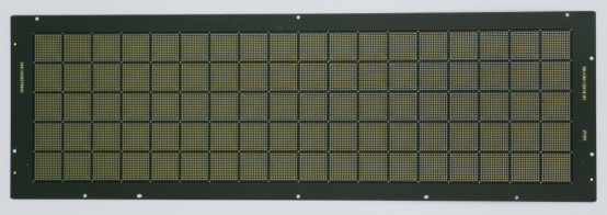
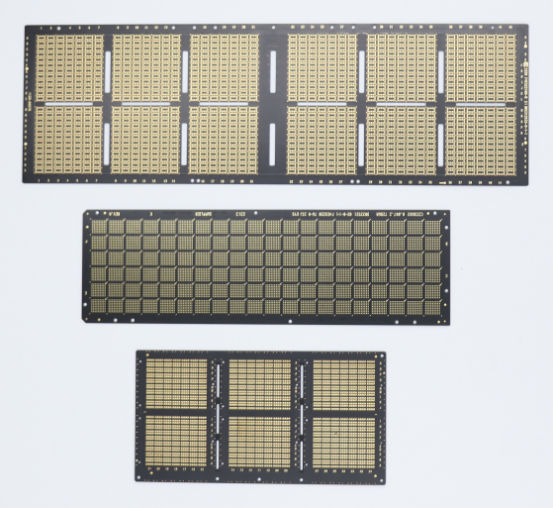
Why IC Substrates Are Essential for Advanced Chip Packaging
In today’s era of advanced semiconductor packaging, shrinking chip geometries and soaring I/O densities are rewriting the rules of electronic design. As devices push for higher performance within tighter spaces, the industry faces a critical challenge: how to create a reliable, ultra-dense bridge between the chip and the outside world. This need has given rise to a material system far more sophisticated than traditional PCB technology—a substrate engineered to manage fine-pitch routing, heat, mechanical stress, and high-speed signals all at once.
IC Substrates: Definition and Origins
The Emergence of IC Substrates and the Evolution of Packaging Technology
IC substrates were introduced in the mid-1990s when packaging technologies such as BGA (Ball Grid Array) and CSP (Chip Scale Package) began to rise. These new formats required far tighter routing density and far smaller interconnect features than traditional PCB processes could provide. As a result, a new type of carrier—capable of supporting ultra-fine lines, high I/O counts, and reliable thermal management—became essential. This is how IC substrates came into existence.
Although IC substrates originated from PCB technology, they are fundamentally more advanced. A conventional PCB focuses on mechanical support and basic electrical routing, while an IC substrate must handle micro-scale interconnects, high-frequency signals, and delicate chip-to-board transitions. Because of these requirements, IC substrates use more precise materials, more controlled dielectric properties, and fabrication processes designed for ultra-fine features.
In semiconductor packaging and testing, the IC substrate plays several critical roles:
Signal connection: It transfers signals between the chip’s microscopic pads and the system-level PCB.
Mechanical support: It holds the bare die in place and protects it during handling and operation.
Thermal dissipation: Its copper structure helps draw heat away from the chip.
Environmental protection: It shields sensitive circuitry from moisture, contamination, and mechanical stress.
These functions make the IC substrate a core component of modern advanced packaging, bridging the gap between semiconductor wafers and larger electronic systems.
Key Differences Between IC Substrates and Traditional PCBs
The fundamental difference between IC substrates and standard PCBs lies in their achievable feature sizes. An IC substrate can typically reach 20 μm / 20 μm line width and spacing, with leading-edge solutions pushing toward 10 μm / 10 μm or even 5 μm / 5 μm. In contrast, most conventional PCBs are limited to ≥50 μm. This difference directly determines the density of interconnects the substrate can support.
IC substrates also deliver higher-density, thinner, and more precise structures. For example, the layer stack of an IC substrate may include multiple build-up layers formed with semi-additive processes, enabling microvias and ultra-thin dielectric layers. A typical application would be a flip-chip processor package, where the substrate must route thousands of fine-pitch bumps within a very small footprint—something a traditional PCB cannot handle.
Material and manufacturing complexity are also significantly higher. IC substrates rely on advanced resin systems such as BT, ABF, or modified epoxies designed for low dielectric loss and high thermal stability. Their fabrication uses SAP or MSAP processes to create micro-scale copper traces, while PCBs usually use subtractive etching that cannot form the same level of precision.
In short, an IC substrate is not simply a “smaller PCB”; it is a purpose-built, high-precision carrier engineered to meet the extreme demands of modern semiconductor packaging.
The Critical Role of IC Substrates in Advanced Packaging
Enabling High-Density Interconnects Between the IC and the PCB
An IC substrate is the main bridge that connects a semiconductor chip to the system-level PCB. Its ability to form ultra-fine copper traces allows it to support extremely high I/O density. This is essential because modern chips may contain thousands of bumps or pads that need to be routed in a very small area. Fine-pitch lines such as 20 μm / 20 μm and below allow the substrate to fan out these signals in a controlled and compact layout.
High-density routing also supports stable high-speed signal transmission. Shorter paths, uniform dielectric materials, and carefully controlled trace geometry help reduce signal loss and maintain timing accuracy. For example, high-speed interfaces such as PCIe, LPDDR, and SerDes rely on consistent impedance and low propagation delay—features that an IC substrate is specifically engineered to deliver.
The substrate further improves system performance by mitigating electromagnetic interference. Features such as ground shielding layers, optimized via structures, and tight trace coupling help reduce noise and crosstalk. As a result, signals travel with higher integrity, which directly enhances the performance and reliability of the entire device.
Supporting Chip Miniaturization and System-Level Integration (SiP, BGA, CSP, FC, MCM)
One of the reasons IC substrates are essential for advanced packaging is their ability to reduce the overall footprint of electronic components. In many advanced packages, the package area can approach a 1:1 ratio with the chip area, allowing devices to remain compact without sacrificing functionality.
IC substrates are compatible with nearly all mainstream packaging formats, including BGA, CSP, flip-chip (FC), and multi-chip module (MCM) designs. Each of these formats requires fine-pitch redistribution and precise vertical interconnect structures—capabilities that standard PCBs cannot deliver.
For SiP (System-in-Package), the requirements are even more demanding. A SiP may contain multiple active and passive components integrated into one compact module. To support this, the IC substrate must provide:
multilayer build-up structures
ultra-low line width and spacing
microvias for vertical routing
controlled dielectric thickness for signal performance
A practical example highlights the difference: an ordinary PCB cannot support the dense, multi-layer routing needed for an RF-SiP module used in a smartphone. In contrast, an IC substrate can accommodate stacked dies, high-density traces, and precise impedance control, enabling full system-level integration within a very small footprint.
Providing Mechanical Support, Thermal Management, and Reliability
Beyond electrical performance, an IC substrate provides essential structural and protective functions. It physically supports the bare chip, dissipates stress generated during operation, and protects fragile internal wiring. Without this mechanical foundation, the chip would be unable to endure handling, assembly, or long-term use.
Thermal management is another key advantage. The copper foil, resin system, and internal layers of the substrate create efficient heat-spreading pathways that draw thermal energy away from the die. This helps maintain stable operating temperatures and prevents heat-induced degradation.
Reliability also depends on material compatibility. IC substrates use low-CTE (Coefficient of Thermal Expansion) materials to minimize the mismatch between the chip, the substrate, and the PCB. By reducing thermal expansion differences, the risk of solder joint cracking and interconnect fatigue decreases significantly. This is especially critical for high-power or high-temperature applications such as AI accelerators, networking chips, and automotive electronics.
Main Classifications of IC Substrates
Classification by Packaging Type
IC substrates are designed to match specific packaging formats. The primary types include:
BGA (Ball Grid Array) Substrates
Designed for high I/O count chips, BGA substrates distribute thousands of connections across an array of solder balls. They are commonly used for processors, memory modules, and graphics chips.
Example: A high-pin-count GPU often uses a BGA substrate to manage dense connections while maintaining reliable electrical performance.
CSP (Chip Scale Package) Substrates
CSP substrates are nearly the same size as the chip itself, minimizing package footprint. They are widely used in mobile devices and compact electronics. CSP substrates support fine-pitch routing and lightweight assembly.
FC (Flip-Chip) Substrates
Flip-chip substrates allow the die to be mounted directly onto the substrate face-down, providing shorter signal paths and better thermal dissipation. They are ideal for high-speed, high-performance processors and graphics chips.
MCM (Multi-Chip Module) Substrates
MCM substrates integrate multiple chips within a single module. They are used in high-performance computing, networking, and system-in-package (SiP) applications.
Example: Standard PCBs cannot support MCM modules due to insufficient routing density, but IC substrates with multilayer build-up structures can handle complex interconnects.
Classification by Material
The choice of substrate material directly affects thermal stability, signal integrity, and mechanical reliability. Main material types include:
Rigid Substrates (BT/ABF)
CTE: ~13–17 ppm/°C
Commonly used in CPU, GPU, and high-performance logic packaging
Provide high mechanical stability and support fine-pitch lines
Flexible Substrates (PI/PE)
CTE: ~13–27 ppm/°C
Ideal for mobile terminals and foldable electronics
Allow bending, lightweight design, and compact layouts
Ceramic Substrates (Al₂O₃, AlN, SiC)
CTE: ~6–8 ppm/°C (lowest among substrate types)
High thermal conductivity and excellent heat resistance
Used for high-power or high-frequency applications such as RF modules or automotive electronics
Classification by Application Field
IC substrates are also categorized according to the type of electronic device or module they support:
Memory Chip Substrates (DRAM/NAND)
Designed for high-density memory modules with reliable signal transmission and thermal control.
RF Module Substrates (5G / Millimeter-Wave)
Optimized for high-frequency performance and low signal loss. Used in wireless communication devices and antennas.
Processor Substrates (CPU/GPU/AI Chips)
Support high I/O density, low impedance, and efficient heat dissipation for computing-intensive applications.
High-Speed Communication Substrates (Networking Chips)
Designed for switches, routers, and data-center chips where signal integrity at high frequency is critical.
MEMS Substrates (Sensors, Micro-Electro-Mechanical Systems)
Accommodate micro-scale devices such as accelerometers, gyroscopes, and environmental sensors, requiring precise mechanical and electrical integration.
Key Materials and Performance Advantages of IC Substrates
The Importance of Ultra-Thin Electrolytic Copper Foil
Electrolytic copper foil is one of the most critical raw materials in IC substrate fabrication. In advanced IC substrates, copper foil thickness can be as low as 1.5 μm, which is much thinner than standard PCB copper layers.
Ultra-thin copper allows the formation of high-density microtraces necessary for fine-pitch interconnects. However, achieving uniform thickness at such a small scale is technically challenging. Any variation in foil thickness can lead to signal integrity issues or defects during manufacturing.
The production of ultra-thin copper foil also increases material costs. Compared to conventional PCB copper, this high-precision foil is more expensive and requires specialized handling and plating techniques. Nevertheless, the use of ultra-thin copper is essential for enabling fine-line routing, high I/O density, and reliable performance in advanced packages such as BGA, FC, and SiP modules.
Comparison of IC Substrate Base Materials (BT, ABF, MIF)
The substrate material determines the mechanical, electrical, and thermal properties of the IC substrate. Key parameters include dielectric constant (Dk), dielectric loss (Df), thermal stability, and processability.
ABF (Ajinomoto Build-up Film)
Low Dk and Df for high-frequency signals
Excellent thermal stability
Widely used in high-end processors and graphics chips (Intel and AMD applications)
Supports ultra-fine line/space features for advanced packaging
BT (Bismaleimide-Triazine Resin)
Moderate Dk/Df suitable for mid- to high-end mobile and memory devices
Good thermal stability and manufacturability
Cost-effective alternative for large-scale production
MIF (Modified Epoxy Film)
Offers balanced electrical and mechanical properties
Sometimes used in specialty or hybrid applications where unique thermal or mechanical requirements exist
By selecting the appropriate base material, engineers can optimize for signal integrity, thermal management, and process yield depending on the application.
Impact of Materials on High-Frequency and High-Speed Performance
Material properties directly affect the signal integrity and reliability of high-speed IC substrates. Low dielectric constant (Dk) and low dielectric loss (Df) are essential for minimizing signal delay, reflection, and attenuation in high-frequency circuits.
In addition, materials must handle thermal and mechanical stress generated during operation. A substrate with poor thermal stability may experience micro-cracking, delamination, or trace deformation, which can compromise high-speed signal paths.
For example, a memory IC operating at multiple gigahertz requires a substrate material that keeps Dk/Df stable across temperature variations. ABF is often chosen for these applications because it maintains consistent electrical properties while preventing signal loss and thermal-induced failures.
IC Substrate Manufacturing Processes: SAP and MSAP
SAP (Semi-Additive Process) Features
The Semi-Additive Process (SAP) is a key technique used to create ultra-fine copper lines in advanced IC substrates. SAP starts with an extremely thin chemical copper seed layer of less than 1.5 μm. This seed layer serves as the foundation for precise copper plating.
SAP is ideal for achieving line width and spacing below 15 μm, making it suitable for high-density packages such as high-end CPUs, GPUs, and flip-chip modules. Its precision comes at a higher cost: the process is more complex, requires stringent process control, and typically results in slightly lower yield compared to less demanding methods.
The SAP process can be summarized in four steps:
1. Seed Layer Deposition – A thin chemical copper layer is applied to the substrate surface.
2. Pattern Formation – Photolithography is used to define the copper line layout.
3. Electroplating – Copper is plated onto the patterned areas to achieve the desired thickness.
4. Seed Layer Removal – The original thin seed copper is etched away, leaving only the plated lines.
This method allows precise fine-line routing and high-density interconnects, which are critical for modern advanced packaging.
MSAP (Modified Semi-Additive Process) Features
The Modified Semi-Additive Process (MSAP) builds on SAP but uses a thicker seed copper layer exceeding 1.5 μm. This modification makes the process more robust and easier to control.
MSAP is typically used for line width and spacing of 20–25 μm, which is suitable for slightly lower-density applications while maintaining high precision. Compared to SAP, MSAP offers:
Higher yield due to more consistent plating
Lower overall cost because it reduces the risk of defects during processing
The key difference between SAP and MSAP is the thickness of the seed copper layer, which directly impacts the minimum line width, plating uniformity, and achievable density.
Why Advanced Packaging Depends on SAP and MSAP
Advanced IC packages require extremely fine-line interconnects, high signal density, and multilayer routing that cannot be achieved with conventional subtractive processes such as standard PCB etching (SGP).
For example:
High-end CPU and GPU substrates often use ABF materials combined with SAP to achieve lines below 15 μm, enabling thousands of high-speed connections within a small footprint.
Ordinary PCB methods are incapable of producing the ultra-fine traces required for modern SiP, flip-chip, or multi-chip modules.
In short, SAP and MSAP are indispensable for high-density, high-performance IC substrates, providing the foundation for reliable, compact, and high-speed advanced packaging.
Conclusion: Why IC Substrates Are Essential for Advanced Packaging
IC substrates are the backbone of modern chip packaging, solving multiple critical challenges:
High-Density Interconnects: Ultra-fine lines enable thousands of chip-to-PCB connections in compact packages like BGA, FC, and SiP.
High-Frequency Signal Support: Low-loss materials and precise copper routing maintain signal integrity for CPUs, GPUs, and AI chips.
System-in-Package (SiP) Integration: Multi-layer structures and microvias allow multiple components in one compact package.
Mechanical Stability & Thermal Management: Low-CTE materials and copper layers protect chips and dissipate heat efficiently.
Foundation for Next-Gen Chiplet/AI Packaging: Essential for high-density, high-performance designs.
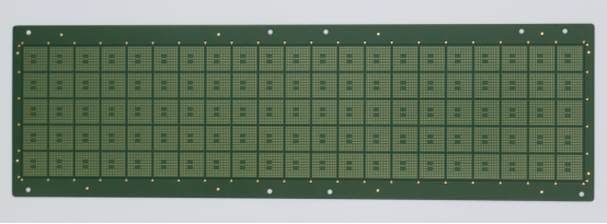
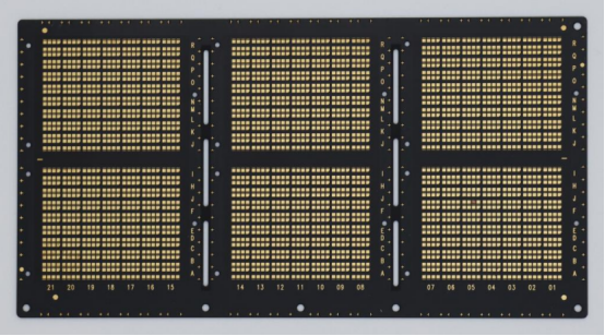
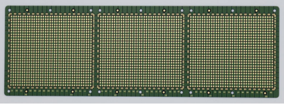
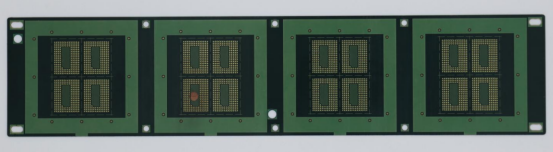
PCBMASTER exemplifies these capabilities through professional IC substrate R&D and manufacturing, combining premium materials, precision fabrication, and full-process quality control. With line widths as small as 25 μm, microvia laser drilling down to 0.05 mm, and AS9100/ROHS certification, PCBMASTER delivers substrates suitable for high-speed, high-density applications across CPUs, GPUs, memory, and SiP modules. Their fast sample lead times (12–30 days) and expert technical team ensure rapid prototyping and scalable production without compromising performance or reliability.
In summary, IC substrates are not optional—they are the critical bridge connecting modern chips to real-world systems, enabling performance, miniaturization, and reliability that standard PCBs cannot provide. Companies like PCBMASTER are at the forefront of making this advanced packaging technology practical and scalable.
FAQs
What are the main differences between IC substrates and regular PCBs?
IC substrates differ from standard PCBs in several critical ways:
Line width and spacing: IC substrates achieve ultra-fine lines, often 20 μm / 20 μm or smaller, while regular PCBs usually have ≥50 μm.
Density and precision: IC substrates support much higher interconnect density and precise multilayer routing.
Materials and processes: IC substrates use advanced materials (ABF, BT, ceramic) and semi-additive fabrication techniques, whereas PCBs typically use standard FR4 and subtractive etching.
Performance: IC substrates handle high-speed, high-frequency signals and better thermal management, while regular PCBs are limited in these aspects.
Why does SiP require IC substrates instead of HDI or traditional PCBs?
System-in-Package (SiP) modules integrate multiple active and passive components in a single compact package. IC substrates are necessary because:
They provide multi-layer routing and microvias to connect dense components.
They allow fine-pitch lines that HDI or standard PCBs cannot reliably achieve.
They maintain signal integrity at high frequencies and offer controlled thermal expansion to prevent mechanical stress.
Example: A smartphone RF-SiP module cannot be implemented on an HDI PCB without compromising performance or reliability.
What are the differences between ABF, BT, and other base materials, and which chips are they suitable for?
ABF (Ajinomoto Build-up Film): Low dielectric constant (Dk), low dielectric loss (Df), excellent thermal stability; ideal for high-end CPUs, GPUs, and advanced logic chips.
BT (Bismaleimide-Triazine Resin): Moderate Dk/Df, good manufacturability; used in mobile devices, memory chips, and mid-to-high-end applications.
MIF or ceramic substrates: Very low CTE (~6–8 ppm/°C), high thermal conductivity; suitable for high-power, high-frequency applications such as RF modules and automotive electronics.
Which is more advanced, SAP or MSAP, and what are the differences?
SAP (Semi-Additive Process): Uses ultra-thin seed copper (<1.5 μm), supports line width/spacing <15 μm, high precision, higher cost, and slightly lower yield.
MSAP (Modified SAP): Uses thicker seed copper (>1.5 μm), supports 20–25 μm lines, easier to manufacture, higher yield, and lower cost.
Key difference: Seed layer thickness determines achievable line width and process complexity.
Conclusion: SAP is more advanced for ultra-fine-line, high-density applications, while MSAP balances cost and yield for slightly larger features.
What are the future trends in IC substrate technology?
Ultra-fine line widths: Pushing below 5 μm for next-gen AI chips and chiplets.
Higher layer counts: Supporting more complex SiP and multi-chip modules.
New materials: Low Dk/Df, high thermal conductivity for high-speed and high-power applications.
Advanced manufacturing: More precise SAP/MSAP, laser direct imaging (LDI), and automated inspection.
Integration with chiplet and AI packaging: IC substrates will remain the foundation for modular, high-performance electronic systems.

