


Vacuum Two-Fluid Etching: Revolutionizing PCB Precision
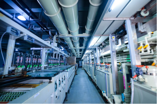
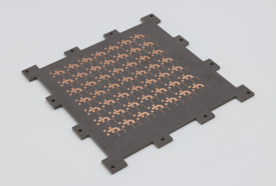
Vacuum Two-Fluid Etching (VTFE) is an advanced method used in PCB (Printed Circuit Board) manufacturing to etch precise and intricate circuit patterns onto the board. The process works by combining two fluids—an etching liquid and a compressed gas—inside a sealed vacuum chamber. This creates a fine mist that is directed onto the PCB to remove unwanted copper or other conductive materials with exceptional precision.
Unlike traditional etching methods, such as spray or immersion etching, which often lead to uneven material removal or over-etching, VTFE controls the etching process more precisely. The vacuum environment eliminates air bubbles and ensures the etchant mist is evenly distributed across the PCB surface, allowing for extremely small traces (as fine as 20 microns or less) and sharp, well-defined edges. This method minimizes defects and waste, making it ideal for modern electronics that require high-density, high-precision circuits.
How Does Vacuum Two-Fluid Etching Work?
Vacuum Two-Fluid Etching (VTFE) combines a vacuum-sealed chamber with a mist of two fluids: an etching liquid and a compressed gas. This combination allows for controlled and uniform material removal, resulting in accurate circuit patterns.
What Are the Core Principles of VTFE?
Vacuum Chamber and Two-Fluid Mist:
The core principle of VTFE lies in the use of a vacuum-sealed chamber. The chamber removes air from the system, creating a controlled environment for etching. Inside, a precise mixture of etching liquid (such as ferric chloride or cupric chloride) and compressed gas (typically nitrogen or air) is sprayed onto the PCB. The mist that forms is highly controlled, with droplets that are only 5-10 microns in size. This fine mist ensures even material removal across the entire PCB surface, even in tight spaces like between layers.
Consistent Spray Mist for Material Removal:
In VTFE, the mist is applied gently and evenly to the PCB, preventing over-etching or under-etching, which can occur with traditional high-pressure spray systems. The even distribution of the mist ensures that the etchant removes material at a consistent rate, achieving sharp, clean circuit patterns. This precise control prevents defects like uneven edges or "tapered" traces, which can compromise the performance of the final PCB.
What Are the Step-by-Step Processes in VTFE?
1. PCB Preparation: The first step in VTFE is to load the PCB into the vacuum-sealed chamber. The PCB is typically coated with a photoresist layer that defines the desired circuit pattern. This photoresist protects certain areas of the board, preventing the etchant from removing material from those sections.
2. Vacuum Activation: Once the PCB is in place, the chamber is evacuated to create a near-perfect vacuum environment (around -95 kPa). This step removes air and moisture, ensuring that no contaminants interfere with the etching process. The vacuum also helps to stabilize the PCB, ensuring that the etchant mist is distributed evenly across the board.
3. Two-Fluid Mist Generation: In this step, a high-precision nozzle combines the etching liquid and compressed gas to form a fine mist. The nozzle is designed to produce droplets that are uniform in size, typically between 5 and 10 microns. This fine mist is crucial for penetrating narrow spaces between multilayer PCBs and ensuring uniform material removal.
4. Controlled Etching Process: As the mist is directed onto the PCB, sensors monitor the etching depth in real-time. The system adjusts the mist pressure and temperature to maintain a consistent etching rate. This precise control ensures that the etching depth is uniform and that the traces have sharp edges. The result is highly accurate and consistent circuit patterns.
5. Rinsing & Drying: After etching, the PCB is rinsed with deionized water to remove any residual etching chemicals. This step ensures that the PCB is clean and free from any contaminants that could affect further processing. Finally, the board is dried using a vacuum-assisted drying process, which removes moisture without damaging the delicate traces.
What Are the Key Components of a VTFE Machine?
Vacuum Chamber:
The vacuum chamber is the heart of the VTFE system. Made from corrosion-resistant stainless steel, it creates a sealed environment where air and contaminants are eliminated. This chamber is crucial for ensuring even distribution of the etchant mist and preventing issues such as air bubbles that could affect the quality of the etching.
Dual-Fluid Nozzles:
The precision nozzle in VTFE machines is designed to spray a fine mist of etchant liquid mixed with compressed gas. These nozzles are ceramic-tipped, preventing clogging and ensuring consistent mist formation, even during continuous operation. The nozzle's design allows for precise control over the mist's pressure and flow, ensuring that the etching process remains uniform.
Real-Time Monitoring:
VTFE machines are equipped with sensors and cameras to monitor the etching process. These sensors track parameters like etching depth, mist distribution, and pressure. The real-time data allows the system to adjust automatically, ensuring consistent and accurate results. This monitoring system reduces the risk of defects and increases yield rates.
Etchant Recycling System:
One of the key advantages of VTFE is its ability to reduce waste. The etchant recycling system captures unused etchant and filters it for reuse. This not only makes the process more environmentally friendly but also reduces operating costs by conserving expensive chemicals. The recycling system ensures that the etchant is used efficiently, contributing to the overall cost-effectiveness of the process.
Why Is Vacuum Two-Fluid Etching Important for PCB Manufacturing?
Vacuum Two-Fluid Etching (VTFE) allows manufacturers to produce circuit traces as thin as 20 microns, far beyond the capabilities of traditional methods. This precision is crucial for industries like telecommunications, aerospace, and medical devices, where even the smallest defect can cause device failure. Additionally, VTFE improves production efficiency by reducing material waste and energy consumption, making it a cost-effective and eco-friendly solution for PCB fabrication.
How Does VTFE Improve Precision in PCB Etching?
Micron-level Precision:
One of the key advantages of VTFE is its ability to achieve micron-level precision in etching. VTFE can etch traces as small as 20 microns with edge accuracy of ±2 microns, which is significantly finer than traditional etching methods. This level of precision is critical for producing PCBs used in high-performance electronics, such as 5G modules and medical devices, where small and precise traces are necessary for optimal functionality. In contrast, traditional methods like spray or immersion etching often result in rough edges and less consistent trace widths, which can cause issues like signal loss or short circuits in sensitive electronics.
Comparison with Traditional Methods:
Compared to spray etching, which typically achieves trace widths of around 50 microns, and immersion etching, which can handle widths of 100 microns or more, VTFE stands out for its ability to achieve much smaller and more consistent trace sizes. Spray etching uses high-pressure nozzles that often cause over-etching, leading to rough edges and tapered traces. Immersion etching, on the other hand, can lead to uneven material removal, especially on multilayer PCBs. VTFE's fine mist and controlled vacuum environment eliminate these issues, resulting in sharper, cleaner edges and uniform etching across the entire board.
How Does VTFE Reduce Waste and Improve Efficiency?
30–40% Less Etchant Usage:
One of the major benefits of VTFE is its reduced etchant usage. The two-fluid mist technology targets only the areas of the PCB that require etching, using up to 30-40% less etchant compared to traditional methods like spray or immersion etching. In traditional etching processes, a significant amount of etchant is wasted either through over-spray or excessive chemical use. By using a controlled mist, VTFE minimizes waste, making the process more efficient and environmentally friendly.
Eco-friendly Benefits: Etchant Recycling and Reduced Chemical Disposal Costs:
VTFE also includes an etchant recycling system that captures unused etchant, filters it, and reuses it in future etching processes. This reduces the need for fresh etchant and significantly cuts down on chemical disposal costs. In addition to minimizing waste, this recycling process makes VTFE a more sustainable option for PCB manufacturers. By reusing etchant, companies can lower their environmental impact and meet stricter regulatory standards regarding waste management.
Energy Savings with Reduced Need for High-Pressure Pumps:
Another way VTFE improves efficiency is by reducing energy consumption. Traditional spray etching methods require high-pressure pumps to distribute the etchant over the PCB surface. These pumps consume a large amount of energy, especially in high-volume production. VTFE, on the other hand, uses a vacuum chamber to create a controlled environment for the etchant mist, reducing the need for energy-intensive pumps. This energy savings can lead to lower operational costs and a smaller carbon footprint for manufacturers.
Vacuum Two-Fluid Etching vs. Traditional Etching: Why is VTFE Superior?
Vacuum Two-Fluid Etching (VTFE) has several key advantages over traditional etching methods, like spray etching and immersion etching. VTFE is specifically designed to handle the challenges of modern electronics, where precision, efficiency, and material conservation are critical. Here’s a detailed comparison of VTFE against traditional methods:
How Does VTFE Compare to Spray Etching?
Trace Width and Edge Accuracy Comparison (20μm vs. 50μm):
One of the most significant differences between VTFE and spray etching is trace width and edge accuracy. VTFE can achieve trace widths as small as 20 microns (μm) with an edge accuracy of ±2μm. This level of precision is crucial for modern electronics, where even a slight deviation can lead to performance issues, such as signal loss or short circuits. In contrast, spray etching typically handles trace widths of around 50μm, with less precise edge accuracy (±10μm). This makes spray etching unsuitable for high-density, high-speed circuits found in applications like 5G and medical devices.
Waste Generation Differences (30–40% Less Etchant):
VTFE is significantly more efficient in etchant usage compared to spray etching. VTFE uses 30–40% less etchant, as it applies a fine mist directly to the areas of the PCB that need etching, minimizing waste. Spray etching, on the other hand, relies on high-pressure sprays that can lead to over-spray and unnecessary chemical usage, increasing waste. This reduction in etchant consumption not only cuts material costs but also makes VTFE more environmentally friendly.
Yield Rates: 99.8% for VTFE vs. 95–97% for Spray Etching:
VTFE's yield rate—the percentage of PCBs produced without defects—reaches up to 99.8%, a significant improvement over traditional spray etching methods, which typically yield only 95–97% defect-free boards. This higher yield is largely due to VTFE's precision and controlled environment, which reduces issues like over-etching and uneven material removal that can result in defects during spray etching. For manufacturers, a higher yield translates to lower rework costs and fewer defective products.
How Does VTFE Outperform Immersion Etching?
Minimum Trace Size Differences: 20μm vs. 100μm:
Another area where VTFE excels is its minimum trace size capability. VTFE can etch traces as fine as 20μm, which is far smaller than the 100μm minimum achievable with immersion etching. Immersion etching is a batch process where the entire PCB is submerged in an etching solution. This method is not precise enough to handle the fine, dense traces required for modern electronics, such as those used in smartphones or wearables. VTFE's fine mist allows for micron-level precision, making it ideal for high-performance applications.
VTFE’s Effectiveness with Multilayer and Non-Standard Materials:
VTFE outperforms immersion etching when it comes to handling multilayer PCBs and non-standard materials. Immersion etching typically struggles with multilayer PCBs, especially when there are blind or buried vias (holes that connect different layers). VTFE, however, can etch 8+ layer PCBs with ease, maintaining uniform etching across layers without damaging inner layers. Additionally, VTFE is highly effective on non-standard materials like ceramic or metal-core PCBs—materials commonly used in aerospace and high-power LED applications. Immersion etching, on the other hand, often causes uneven etching on these materials or leads to warping due to the chemical bath's temperature and pressure.
Comparison Table: VTFE vs. Traditional Etching Methods
Feature Vacuum Two-Fluid Etching (VTFE) Spray Etching Immersion Etching Minimum Trace Width 20μm 50μm 100μm Edge Accuracy ±2μm ±10μm ±15μm Etchant Usage 30–40% less than spray etching High waste High waste Yield Rate 99.8% 95–97% 90–93% Multilayer Support 8+ layers Up to 4 layers Up to 2 layers Non-Standard Materials Works with ceramic, metal-core Limited to FR4 Not recommended Cost per Unit (High-Volume) $0.15–$0.25/cm² $0.12–$0.20/cm² $0.08–$0.15/cm²
What Are the Key Advantages of Vacuum Two-Fluid Etching?
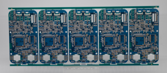
Vacuum Two-Fluid Etching (VTFE) is revolutionizing the PCB manufacturing process, offering several key advantages over traditional etching methods. These benefits include micron-level precision, efficiency in material use, reduced waste, and better handling of complex designs. By leveraging a vacuum environment and a gas-liquid mist, VTFE ensures cleaner, sharper, and more accurate etching results, making it the ideal choice for producing high-performance electronics. Below, we’ll explore these key advantages in more detail.
How Does VTFE Enable Micron-Level Precision?
Sharp Edges and Consistent Traces:
One of the standout features of VTFE is its ability to produce sharp edges and consistent traces at micron-level precision. This is achieved through a controlled mist of etchant, which removes material evenly across the PCB surface. The result is traces as small as 20μm with ±2μm edge accuracy—significantly better than traditional methods like spray etching, which can leave "fuzzy" or tapered traces. Sharp, clean traces are crucial for high-performance devices, where signal integrity and reliability are paramount.
Example Applications: 5G and High-Frequency Circuits:
VTFE's precision is especially important for 5G and high-frequency circuits. In these applications, the need for finely etched traces and sharp edges is critical to prevent signal degradation and interference. For example, 5G networks rely on PCBs with very fine traces to handle high-frequency signals (28 GHz and beyond). Traditional etching methods, which produce rougher edges, would impair signal quality and reduce the efficiency of high-speed circuits. VTFE ensures the clean, precise etching required for these applications, resulting in faster, more reliable connections.
Comparison with Traditional Spray Etching’s “Fuzzy” or Tapered Traces:
In contrast to VTFE, spray etching often leads to traces with tapered edges and uneven widths. These "fuzzy" or irregular traces can cause problems in high-speed circuits, where even minor imperfections can affect performance. VTFE’s precise, uniform etching prevents these issues, making it a superior choice for high-density, high-speed designs.
How Does VTFE Support Complex PCB Designs?
Capability to Handle 8+ Layer Multilayer PCBs and HDI Boards:
VTFE shines in its ability to handle complex PCB designs—especially multilayer PCBs (MLBs) with 8 or more layers. Traditional etching methods, such as spray or immersion etching, often struggle with multilayer designs, especially when it comes to blind vias (holes connecting different layers). VTFE, on the other hand, allows for precise etching through all layers of the PCB, ensuring uniform etching and alignment without damaging inner layers. This makes it perfect for applications that require intricate, multi-layered circuit boards, like smartphones, wearables, and high-end electronics.
Flexibility with Non-Standard Materials Like Ceramic and Metal-Core PCBs:
Another significant advantage of VTFE is its flexibility with non-standard materials. Traditional etching processes can damage or etch non-standard materials unevenly, such as ceramic or metal-core PCBs. These materials are commonly used in high-power or high-frequency applications like aerospace and LED lighting, where heat dissipation and durability are critical. VTFE, with its controlled mist, can etch these materials with precision, maintaining their integrity while creating the necessary circuit patterns. This capability expands design possibilities and supports a wider range of industries and applications.
Why Is VTFE More Cost-Effective in the Long Term?
Upfront Cost vs. ROI: High-Quality Output with Fewer Defects Reduces Rework:
While VTFE machines have a higher upfront cost compared to traditional etching systems, their superior performance leads to greater long-term savings. VTFE offers a yield rate of 99.8%, meaning fewer defective PCBs and less need for rework. For a manufacturer, this higher yield means reduced scrap rates, fewer warranty claims, and less need for manual corrections. Over time, this translates into significant savings in both labor and material costs. For example, a company producing 10,000 PCBs might save thousands of dollars by avoiding rework and improving production efficiency with VTFE.
Reduced Waste and Energy Savings Make VTFE a Smart Investment for High-Volume Production:
VTFE also helps manufacturers cut costs by reducing etchant waste and energy consumption. The method uses up to 40% less etchant than traditional spray etching, and it recycles the unused etchant, making it a more eco-friendly option. Additionally, VTFE requires less energy than spray etching, which relies on high-pressure pumps. By saving both on materials and energy, VTFE can lead to significant cost reductions over time, especially for high-volume production. For example, a manufacturer using VTFE could save $15,000–$20,000 in etchant costs annually, making the investment in VTFE equipment pay for itself in a matter of months.
Real-World Applications of VTFE Technology
Vacuum Two-Fluid Etching (VTFE) is transforming multiple industries by offering precision, efficiency, and versatility in PCB manufacturing. This innovative technology is making waves across various sectors, including aerospace, telecom, and healthcare. Below, we dive into how VTFE is shaping these fields and driving advancements in electronic design and production.
How Does VTFE Impact Aerospace?
Precision for Satellite PCBs and Aircraft Avionics:
In the aerospace industry, PCB precision is crucial, especially for satellite and aircraft avionics. These systems rely on circuit boards that must withstand extreme conditions while ensuring flawless performance. VTFE excels in creating precise traces for aerospace PCBs, ensuring reliable signal transmission even in the most demanding environments. For instance, VTFE can etch 20μm traces with ±2μm edge accuracy, essential for ensuring the integrity and functionality of avionics systems used in aircraft or space missions.
Ability to Withstand Extreme Conditions:
Aerospace PCBs face extreme environmental stress, such as thermal cycling (extreme temperature fluctuations) and vibration during flight. VTFE’s high precision ensures that the etching is uniform and the traces remain intact despite these stresses. This makes VTFE-etched PCBs ideal for use in satellites and space exploration vehicles, where reliability is non-negotiable. For example, VTFE is used in satellite communication systems, where the boards must survive temperatures ranging from -50°C to 125°C, without experiencing trace misalignment or failure.
Why Is VTFE Critical for Telecom and 5G?
Meeting the Requirements for Ultra-Dense Traces and High-Frequency Signals in 5G Modules:
As telecom companies roll out 5G networks, the demand for high-density PCBs with ultra-fine traces has skyrocketed. VTFE is ideally suited for this task because it can achieve trace widths as narrow as 20μm, with precise edge accuracy. These fine traces are necessary for 5G circuits, which carry high-frequency signals (e.g., 28 GHz and higher) without degradation. The ability to produce these tiny, micron-level traces ensures that 5G modules are capable of transmitting large amounts of data with minimal signal loss.
Example of a 5G Base Station PCB Requiring Trace Widths as Small as 30μm:
One example of VTFE’s importance in telecom is the etching of 5G base station PCBs. These modules must handle the demands of next-gen telecommunications, requiring traces as small as 30μm to fit high-speed signal paths in a compact, efficient design. VTFE’s precision allows manufacturers to produce these PCBs with clean, sharp traces, ensuring optimal signal integrity and minimized interference. Traditional etching methods, such as spray etching, struggle with such fine features, leading to higher signal loss and lower performance in 5G networks.
How Does VTFE Improve Medical PCB Production?
Tiny, Reliable Traces for Life-Saving Medical Devices Like Pacemakers and MRI Machines:
In the medical industry, PCBs are used in devices that are often life-saving, such as pacemakers, MRI machines, and implantable medical devices. These devices require extremely precise etching to ensure that the circuits perform correctly under critical conditions. VTFE enables the production of tiny traces as small as 20μm, essential for maintaining the performance of these sensitive medical devices. These devices depend on PCB circuits that must operate flawlessly for many years, so reliable, defect-free etching is essential.
Clean Etching Process for Sterile Environments:
VTFE’s controlled, vacuum-based process also provides a significant advantage in medical PCB production because it ensures a clean and sterile environment. Traditional etching methods can leave behind contaminants that can affect the safety and performance of medical devices. The vacuum chamber in VTFE eliminates dust, air bubbles, and other contaminants during the etching process, ensuring that PCBs are free from impurities that might interfere with their functioning. For example, MRI machines rely on PCBs that must maintain their precision and integrity without introducing contamination, which could compromise the equipment's effectiveness.
Conclusion: The Future of PCB Manufacturing with VTFE Technology
Vacuum Two-Fluid Etching (VTFE) has already revolutionized the PCB manufacturing process, setting a new standard for precision, efficiency, and sustainability. By enabling the production of highly detailed circuit boards with micron-level accuracy, VTFE is transforming industries such as aerospace, telecommunications, and healthcare. From creating small, reliable traces for 5G modules to ensuring the performance of mission-critical aerospace components and life-saving medical devices, VTFE is shaping the future of electronics.
The benefits of VTFE extend beyond its superior precision—it also reduces waste, minimizes energy consumption, and enhances overall production efficiency. For manufacturers looking to stay competitive, adopting VTFE technology means higher-quality output, fewer defects, and a more sustainable approach to PCB production. Companies like PCBMASTER are already leading the way by integrating cutting-edge technologies, including VTFE, to produce high-reliability PCBs tailored to meet the needs of industries that demand the best.
As the demand for smaller, faster, and more precise electronics continues to grow, VTFE is not just a technology of the future—it’s already paving the way for the next generation of advanced PCB manufacturing.
FAQs
Is VTFE more expensive than traditional etching methods?
Yes, VTFE requires a higher initial investment compared to traditional etching methods like spray and immersion etching. The machines are more advanced, and the setup costs are typically 2-3 times higher. However, the long-term savings make VTFE a more cost-effective choice for high-volume production. The technology results in higher yields, lower defect rates, and reduced rework costs, which ultimately offset the initial expense. Additionally, VTFE reduces etchant waste by 30-40% and energy usage, further improving the overall cost-effectiveness over time.
Can VTFE etch materials other than copper?
Yes, VTFE is highly versatile and can etch a wide range of materials besides copper. It works well with ceramic, aluminum, nickel, and other metals, making it suitable for various non-standard PCBs. This flexibility allows manufacturers to create PCBs with different materials tailored for specific applications, such as metal-core PCBs used in high-power electronics or ceramic PCBs used in aerospace components. Traditional etching methods often struggle with these materials, but VTFE maintains high precision regardless of the substrate.
What’s the minimum trace size VTFE can etch?
VTFE can achieve extremely fine trace widths as small as 15μm, with edge accuracy of ±1μm. This level of precision makes it ideal for high-density interconnects (HDI) and applications that demand the utmost precision, such as 5G and high-frequency circuits. Traditional etching methods typically fall short in achieving such fine details, often resulting in rough or tapered traces. VTFE’s capability to maintain sharp, clean edges ensures that critical signals are transmitted without distortion.
Can VTFE be used for small-batch production?
Yes, VTFE is flexible enough for small-batch production, including quick-turn prototyping. While it shines in high-volume PCB production, it can also be utilized for small-batch orders (e.g., 10-100 PCBs) with fast turnaround times. This makes VTFE an excellent choice for companies needing rapid prototyping and small production runs, allowing for customized, high-quality PCBs even in low quantities.
How does VTFE improve PCB reliability?
VTFE enhances PCB reliability by ensuring precision in the etching process, leading to cleaner, more consistent traces. This reduces the likelihood of defects like under-etching or over-etching, which can cause shorts, signal loss, or circuit failure. With VTFE’s micron-level accuracy and uniform material removal, PCBs are less prone to performance degradation. As a result, VTFE-etched PCBs offer long-lasting performance, even in critical applications like medical devices or aerospace systems, where failure is not an option.
Author Bio
Hi, I'm Carol, the Overseas Marketing Manager at PCBMASTER, where I focus on expanding international markets and researching PCB and PCBA solutions. Since 2020, I've been deeply involved in helping our company collaborate with global clients, addressing their technical and production needs in the PCB and PCBA sectors. Over these years, I've gained extensive experience and developed a deeper understanding of industry trends, challenges, and technological innovations.
Outside of work, I'm passionate about writing and enjoy sharing industry insights, market developments, and practical tips through my blog. I hope my posts can help you better understand the PCB and PCBA industries and maybe even offer some valuable takeaways. Of course, if you have any thoughts or questions, feel free to leave a comment below—I'd love to hear from you and discuss further!

