


PCB Burn-In Test Temperatures for Reliable Electronics: A Complete Guide
Reliability is essential in every electronic device, and PCBs are no different. Early failures in circuit boards can lead to costly repairs, customer dissatisfaction, and loss of trust. Burn-in testing helps identify weak components before they reach the consumer, but getting the temperature right is critical. If the temperature is too low, defects can go unnoticed; too high, and you risk damaging the board. Finding the right balance is key to ensuring that only the most reliable PCBs make it to the market.
What is PCB Burn-In Testing?
PCB burn-in testing is a method used to stress-test printed circuit boards (PCBs) by exposing them to elevated temperatures, and sometimes increased voltages, to accelerate the aging process of weak components. The purpose of this testing is to identify and eliminate early failures before the PCBs reach consumers or are integrated into products. By simulating real-world stresses, burn-in testing helps ensure that only reliable PCBs are shipped to the market.
The process works by exposing the PCB to conditions that mimic the operational environment, pushing the components to their limits. This helps reveal any latent defects, such as faulty solder joints, weak capacitors, or low-quality resistors, that might otherwise fail under normal use after a longer period.
For example, a PCB used in consumer electronics like smartphones might undergo burn-in testing at a temperature of 100°C for 16 hours. This stresses the components in a way that might reveal weak points, preventing those defects from causing failures in the field.
Why Does Temperature Matter in PCB Burn-In Testing?
Temperature plays a critical role in PCB burn-in testing because it accelerates the aging process of components. By increasing the temperature, weak or defective components fail faster, allowing manufacturers to identify potential issues before the product reaches the consumer. When components are exposed to higher temperatures, they experience more stress, simulating the conditions they would face during real-world use. This "stress testing" helps to uncover weaknesses like poor solder joints, low-quality capacitors, or faulty resistors that could cause the PCB to fail prematurely.
For instance, a PCB designed for a smartphone might have components that can handle typical operating conditions, but if exposed to higher temperatures during testing, the weaknesses in some components will show up more quickly. This allows the manufacturer to fix these issues early in the production process, ensuring only reliable units are shipped to customers.
What is the Ideal Burn-In Temperature Range for Different Applications?
Burn-in testing ensures that PCBs are reliable under real-world conditions, but the ideal testing temperature varies depending on the application. Each industry has specific standards that help balance defect detection and component protection. Below are the optimal temperature ranges for different types of PCBs and their associated goals.
Consumer Electronics: 90°C–125°C (IPC-9701 standards) for Phones, IoT Devices, and TVs
Goal: The primary goal in consumer electronics burn-in testing is to identify weak capacitors, solder joints, and microchips that could cause premature failure.
Why this range?
Consumer electronics, such as smartphones, smart home devices, and televisions, are often used in controlled indoor environments where the temperature rarely exceeds 30–40°C. Burn-in testing in the 90°C–125°C range simulates this typical use scenario while accelerating the failure of components that might be prone to early failures. This temperature range is high enough to push components beyond their normal operating limits but not so extreme as to damage the boards themselves.
Example:
For a smartphone PCB, burn-in testing at 100°C for 16 hours is common. This helps to catch issues like weak solder joints or defective capacitors before the device reaches consumers. A weak capacitor may not fail immediately but could cause system instability after months of use, so testing ensures only reliable devices are shipped.
Industrial Equipment: 100°C–135°C (MIL-STD-202G) for Factory Controllers, Sensors, Motors
Goal: In industrial settings, burn-in testing ensures that PCBs will perform reliably under the extended operational hours and stress of factory environments.
Why this range?
Industrial equipment, including factory controllers, sensors, and motors, operates in environments where equipment can be on 24/7, facing continuous cycles of heat and mechanical stress. The 100°C–135°C temperature range is ideal for identifying weak components in these high-stress, high-demand environments. It ensures the PCBs can withstand long hours of use without failures.
Example:
For factory controllers, burn-in testing at 125°C for 48 hours simulates extended operation. This ensures the PCB can handle the constant load of controlling machines, as well as temperature fluctuations that are common in industrial environments. Components like resistors and capacitors in these controllers are stressed to reveal latent defects, preventing future breakdowns.
Automotive PCBs: 125°C–140°C (AEC-Q100 standards) for Underhood Electronics
Goal: Automotive burn-in testing focuses on ensuring the PCB can withstand high engine heat and vibrations commonly found in underhood electronics.
Why this range?
Automotive PCBs, especially those used in engine control units or sensors, must be durable enough to survive the harsh conditions under the hood. The 125°C–140°C range is aligned with the AEC-Q100 standards, which cater specifically to automotive electronics. Testing within this temperature range helps identify weaknesses in components that could fail due to high heat or constant vibration over time.
Example:
An engine control unit PCB may undergo burn-in testing at 135°C for 72 hours. This helps simulate the extreme heat (up to 120°C under normal operation) and constant vibration that these parts are exposed to under the hood. By stress-testing at these temperatures, manufacturers can ensure that the components remain functional throughout the life of the vehicle.
Aerospace: 125°C–150°C (MIL-STD-202G) for High-Reliability Systems like Satellites and Radars
Goal: The goal in aerospace applications is to simulate extreme environmental conditions that the PCB may encounter in space, on aircraft.
Why this range?
Aerospace systems require the highest reliability because failure in these environments can lead to catastrophic results. 125°C–150°C is the ideal temperature range for burn-in testing in these applications, as it simulates extreme conditions such as high altitudes, rapid temperature changes, and exposure to radiation. Testing within this range ensures that the PCB can function reliably even in the most demanding and unpredictable environments.
Example:
A radar PCB might undergo burn-in testing at 150°C for 120 hours, ensuring it can withstand the harsh conditions of being in satellite. These components are exposed to extreme temperatures, vibrations, and potential radiation in space, so burn-in testing ensures that only the most durable, defect-free boards make it into these critical systems.
Comparison Table: Ideal Burn-In Temperature Ranges for Different Applications
Application Temperature Range Standards Goal Consumer Electronics 90°C – 125°C IPC-9701 Catch weak capacitors, solder joints, and microchips Industrial Equipment 100°C – 135°C MIL-STD-202G Ensure reliability in factory settings with extended operational hours Automotive PCBs 125°C – 140°C AEC-Q100 Withstand engine heat and vibration Aerospace 125°C – 150°C MIL-STD-202G Simulate extreme environmental stress conditions
How Do PCB Materials Affect Burn-In Testing Temperature?
The material used in a PCB plays a crucial role in determining the maximum temperature it can safely withstand during burn-in testing. Since different materials have varying levels of heat resistance, understanding how a PCB's Glass Transition Temperature (Tg) affects its burn-in limits is essential. By knowing the Tg of the material, manufacturers can set appropriate testing temperatures to ensure the board undergoes enough stress to identify defects without risking damage to the PCB itself.
Glass Transition Temperature (Tg): Understanding How Tg Determines the Maximum Safe Burn-In Temperature for Different PCB Materials
The Glass Transition Temperature (Tg) is the key factor that determines how much heat a PCB material can safely endure during burn-in testing. Tg represents the temperature at which the material changes from a rigid, glass-like state to a more flexible, rubber-like state. When a PCB is heated beyond its Tg, the material can soften, leading to warping, delamination (layer separation), or even total failure of the board. Therefore, knowing the Tg of the PCB material is critical to setting the correct burn-in temperature to avoid damaging the board.
Standard FR-4: 130°C–140°C Tg, Limits Burn-In to 90°C–125°C
FR-4 is the most common material used in consumer electronics and general-purpose PCBs. With a Tg in the range of 130°C–140°C, FR-4 can safely withstand burn-in temperatures between 90°C and 125°C. Going above these temperatures risks softening the material, which can cause physical damage to the board, such as warping or the separation of its layers. Therefore, FR-4 is ideal for standard applications like smartphones, televisions, and other consumer electronics that don't require extreme temperature testing.
Example:
A PCB made with standard FR-4 is often tested at 100°C for 16 hours in consumer electronics. This stress test identifies weak capacitors and solder joints without exceeding the material's safe thermal limits, ensuring that the board won't be damaged.
High-Tg FR-4: 150°C–180°C Tg, Allows Higher Temperatures Like 125°C–150°C
For applications that require higher burn-in temperatures, high-Tg FR-4 is used. This material has a Tg in the range of 150°C to 180°C, allowing for higher testing temperatures such as 125°C to 150°C. High-Tg FR-4 is typically used in industries like automotive and industrial equipment, where PCBs need to handle harsher conditions, such as elevated temperatures and prolonged exposure to stress. The higher Tg gives the material additional strength and heat resistance, making it suitable for more demanding applications.
Example:
A high-Tg FR-4 PCB used in an automotive engine control unit might undergo burn-in testing at 135°C for 72 hours to ensure the components can withstand extreme under-the-hood temperatures, vibrations, and other environmental stressors.
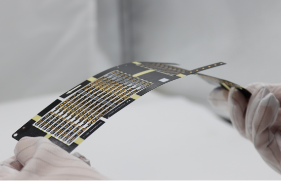
Polyimide & Ceramic Materials: Suitable for Extreme Conditions in Aerospace (Tg >250°C)
For even more extreme applications, polyimide and ceramic materials are used in PCBs that will operate in aerospace environments, where temperatures can reach very high levels. Both polyimide and ceramic materials have Tg values greater than 250°C, making them ideal for applications that experience extreme temperature variations, such as satellites, radar systems, and other high-reliability aerospace systems.
These materials are built to withstand temperatures far beyond what FR-4 can handle, allowing them to be tested at 150°C to 180°C during burn-in testing. This ensures that the PCBs will perform reliably even under the harshest conditions, such as those encountered in space.
Example:
In aerospace, ceramic PCBs used in satellites undergo burn-in testing at temperatures as high as 180°C for 72 hours to ensure they will remain stable in the extreme environment of space, where temperature fluctuations can be drastic.
80% Rule for Safe Temperature: Never Exceed 80% of the Material’s Tg to Avoid Warping and Delamination
A critical rule to follow when performing burn-in testing is the 80% Rule, which suggests that the temperature used during testing should never exceed 80% of the material’s Tg. This rule is designed to prevent the PCB material from reaching the point where it starts to soften, which can lead to warping, delamination, or other forms of damage. By following this rule, manufacturers ensure that the PCB is stressed enough to reveal weak components but not pushed beyond the material’s limits.
Example:
If a PCB is made from high-Tg FR-4 with a Tg of 160°C, the maximum safe burn-in temperature according to the 80% rule would be 128°C (0.8 × 160°C). Testing beyond this temperature could risk damaging the board, even if the components appear fine during testing.
Comparison Table: How Different PCB Materials Affect Burn-In Testing Temperature
PCB Material Glass Transition Temperature (Tg) Safe Burn-In Temperature Range Example Applications Standard FR-4 130°C – 140°C 90°C – 125°C Consumer electronics (smartphones, TVs, IoT) High-Tg FR-4 150°C – 180°C 125°C – 150°C Automotive, industrial equipment Polyimide & Ceramic >250°C 150°C – 180°C Aerospace
How Long Should Burn-In Testing Last?
The duration of burn-in testing plays a critical role in identifying potential weak points in a PCB without damaging it. While the testing temperature is essential, the length of time spent under these conditions is equally important. Too short a test may miss subtle defects, while too long can lead to unnecessary costs and potential damage. The right duration depends on the application, with different industries requiring different testing times to ensure reliability.
Consumer Electronics: 8–24 Hours at 90°C–125°C
Burn-in testing for consumer electronics typically lasts between 8 to 24 hours, depending on the temperature range of 90°C to 125°C.
Why this duration?
Consumer electronics, like smartphones, smart home devices, and TVs, have relatively lower reliability demands compared to more industrial. These devices typically undergo burn-in testing at temperatures ranging from 90°C to 125°C, with testing durations between 8 to 24 hours. This timeframe is long enough to stress the components and catch potential failures, like weak solder joints or capacitors, but short enough to avoid unnecessary costs.
Example:
A smartphone PCB might undergo burn-in testing at 100°C for 16 hours to ensure that weak components, such as faulty microchips or poorly soldered connections, are identified before reaching customers. If no failures occur within this window, the board is likely to be reliable for long-term use.
Industrial Equipment: 24–48 Hours at 100°C–135°C
For industrial equipment, burn-in testing should last between 24 to 48 hours at 100°C to 135°C.
Why this duration?
Industrial equipment, such as factory controllers, sensors, and motors, is subject to continuous, extended operation in often harsh environments. Burn-in testing in this case requires a longer duration to ensure that the components are robust enough to withstand long hours of stress. The 24 to 48-hour testing period at 100°C to 135°C helps simulate the extended operational cycles typical in industrial settings.
Example:
A factory motor controller might undergo 48 hours of burn-in testing at 125°C to ensure it will work reliably over extended periods in real-world factory settings, where machines are constantly running, and temperatures can fluctuate.
Automotive & Aerospace: 48–120 Hours at 125°C–150°C
Automotive and aerospace PCBs require burn-in testing for 48 to 120 hours at higher temperatures between 125°C and 150°C.
Why this duration?
PCBs used in automotive and aerospace applications must endure extreme environments, including high temperatures, vibrations, and other stresses. The longer burn-in test durations ensure that the components can withstand prolonged exposure to these conditions. For automotive electronics (e.g., engine control units) or erospace systems (e.g., satellites and radars), burn-in testing between 48 and 120 hours is necessary to validate the components' performance over extended operational periods.
Example:
A radar PCB could undergo 120 hours of testing at 150°C to simulate the extreme conditions of a combat zone or space environment. The longer duration ensures that the PCB will remain fully operational even under the harshest conditions.
Finding the Right Duration: Don’t Overtest—Test Until Failure Rates Plateau
The key to burn-in testing duration is to avoid overtesting. Testing should continue until failure rates plateau, meaning no new defects are identified.
Why is this important?
The main objective of burn-in testing is to catch weak components before they reach customers, but it’s crucial to avoid wasting resources by testing for longer than necessary. Once failure rates plateau, meaning no new failures occur after a certain time, further testing becomes redundant and costly. The ideal duration is the time it takes for failures to stop appearing, which varies depending on the complexity of the PCB and the application.
Example:
If a burn-in test at 100°C for 24 hours reveals no failures, it’s unlikely that continuing the test for another 24 hours will uncover additional defects. Therefore, testing should stop once the failure rate has stabilized, ensuring both efficiency and cost-effectiveness.
Comparison Table: Burn-In Testing Duration by Application
Application Temperature Range Duration Goal Consumer Electronics 90°C – 125°C 8–24 hours Catch weak solder joints, capacitors, and microchips Industrial Equipment 100°C – 135°C 24–48 hours Ensure reliability under extended operational hours Automotive/Aerospace 125°C – 150°C 48–120 hours Simulate extreme environmental conditions and ensure long-term reliability Finding the Right Duration Depends on failures Test until failure rates plateau Avoid overtesting and reduce unnecessary costs
What Are the Risks of Incorrect Burn-In Temperatures?
Choosing the right temperature for burn-in testing is essential for identifying weak components without damaging the PCB. Incorrect temperatures can lead to overstress, undertesting, or thermal management failures, all of which compromise the reliability of the PCB and increase costs. Let’s break down the risks of incorrect burn-in temperatures.
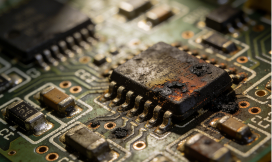
Overstress: The Consequences of Testing at Too High Temperatures (Delamination, Warping)
Testing at too high temperatures can cause physical damage to the PCB, such as delamination and warping, which compromises its integrity.
Why this happens:
When the burn-in temperature exceeds the safe limit for the PCB material, it can cause the board to soften, leading to delamination (separation of the layers) and warping (bending or distortion). This damage is permanent and can result in a non-functional or unreliable PCB. Materials like FR-4 and high-Tg FR-4 have specific temperature limits, and pushing these beyond their tolerance during testing risks damaging the PCB beyond repair.
Example:
Testing a standard FR-4 PCB at 150°C (above its safe limit of 125°C) could cause the layers to separate, rendering the PCB unusable. This could lead to significant production losses and delayed delivery times.
Undertesting: The Risks of Testing at Too Low Temperatures (Undetected Defects, Weak Components)
Testing at temperatures that are too low can result in undetected defects and weak components, leading to early failures once the PCB is in use.
Why this happens:
Low temperatures (below the recommended burn-in range) do not apply enough stress to the PCB, which means weak components—like poor solder joints, low-quality capacitors, or faulty microchips—may remain undetected. If the PCB doesn’t undergo sufficient thermal stress, these weak points won’t fail during testing, leading to early failures in real-world use.
Example:
Testing a consumer electronics PCB at 80°C instead of the required 90°C–125°C would likely leave weak capacitors or solder joints undetected. As a result, the product may fail within a few months after being shipped to customers, leading to costly warranty claims.
Thermal Management Failures: How Poor Heat Distribution Can Skew Results and Cause Inaccurate Conclusions
Poor heat distribution during burn-in testing can cause temperature imbalances, leading to incorrect test results and misleading conclusions about a PCB’s reliability.
Why this happens:
If the heat is not evenly distributed across the PCB during testing, certain components may experience higher temperatures than others, leading to hot spots. These temperature imbalances can cause some areas of the PCB to fail prematurely, while other areas may pass the test despite having weak components. This thermal management failure skews the results and makes it difficult to assess the true reliability of the PCB.
Example:
During a burn-in test for an industrial PCB, a voltage regulator could experience a hot spot if it is located near the edge of the chamber where the temperature is higher. While the rest of the board may remain at the expected temperature, this specific component could fail, but the test could incorrectly pass the entire PCB due to thermal inconsistency.
How Can Data from Burn-In Testing Improve PCB Reliability?
Burn-in testing doesn’t just help identify weak components—it also provides valuable data that can be used to enhance PCB designs, optimize component selection, and ultimately improve the long-term reliability of the product. Here’s how the data collected during burn-in testing can be leveraged to make these improvements.
Identify Weak Points: Pinpoint Common Failure Modes and Component Weaknesses
Burn-in testing data helps identify weak components like capacitors, solder joints, and microchips by tracking failures during stress tests.
Why this matters:
By analyzing failure data from burn-in tests, manufacturers can identify the common failure modes that occur under stress conditions. These failures could be related to specific components like capacitors, solder joints, or microchips. For example, poor soldering might result in joint fractures, or weak capacitors could lead to electrical instability. Pinpointing these weak spots is crucial for improving future designs and preventing these components from causing early failures in real-world use.
Example:
If burn-in testing of a consumer electronics PCB shows a high failure rate of solder joints, the data would indicate that soldering quality needs to be improved. Manufacturers might consider changing their soldering process or using a different soldering material to improve long-term durability.
Optimize Designs: Use Data to Refine PCB Designs for Better Heat Dissipation and Durability
Data from burn-in testing can help refine PCB designs by identifying areas for improved heat dissipation and better durability.
Why this matters:
PCBs often fail because certain areas overheat or lack adequate thermal management. By analyzing the data from burn-in testing, engineers can identify hot spots where temperature control is insufficient. This information can guide the redesign of the PCB to improve heat dissipation through the addition of thermal vias, heat sinks, or better component placement. A well-optimized design helps ensure that the PCB can withstand high temperatures without failing prematurely.
Example:
During burn-in testing, if a voltage regulator on a PCB repeatedly fails due to heat, the design can be modified to include thermal vias that redirect heat away from sensitive components. This would prevent future failures and enhance the PCB’s overall durability.
Improve Component Selection: Track Component Failure Rates to Improve Supply Chain Decisions
Tracking component failure rates during burn-in tests helps manufacturers make better decisions about component selection and supplier choices.
Why this matters:
By analyzing the performance of components under stress, manufacturers can identify parts that fail more frequently than expected. This allows them to make informed decisions when choosing suppliers and components for future production. If certain components show a high failure rate during testing, manufacturers can switch suppliers or opt for higher-quality alternatives to avoid potential problems in the field.
Example:
If resistors from a particular supplier fail frequently during burn-in testing, manufacturers might choose to switch to a different supplier with a better track record for reliability. This helps prevent defects from being built into future PCB assemblies and ensures long-term reliability.
What Are the Key Burn-In Testing Best Practices?
Burn-in testing is a crucial step in ensuring the reliability of PCBs, but to achieve accurate and meaningful results, best practices must be followed. These practices ensure that the testing process is thorough, consistent, and effective in identifying weak components while avoiding damage to the board. Below are the key burn-in testing best practices to follow.
Control Temperature Accurately: Use Closed-Loop Chambers to Maintain Precise Temperatures (±2°C) and Avoid Hot Spots
Accurate temperature control is vital in burn-in testing to avoid skewed results and damage to PCBs. Closed-loop chambers maintain a stable temperature to ensure uniformity.
Why this matters:
Temperature is the most important variable in burn-in testing. Closed-loop chambers are designed to maintain a precise temperature, typically within a ±2°C range, ensuring that the entire PCB is subjected to consistent thermal conditions. This accuracy prevents hot spots—areas where components experience much higher temperatures than the rest of the board. Hot spots can lead to premature component failure or incorrect test results, as some parts of the PCB may fail while others appear fine.
Example:
In a consumer electronics burn-in test, using a closed-loop chamber ensures that all components on the PCB experience uniform temperatures, avoiding misleading results caused by parts of the board being subjected to temperatures that are either too high or too low.
Use Thermal Management Tools: Implement Thermal Vias, Heat Sinks, and Proper Component Placement to Improve Heat Distribution
To prevent heat buildup in critical areas, thermal management tools like thermal vias, heat sinks, and strategic component placement are essential for balanced heat distribution during burn-in testing.
Why this matters:
Heat distribution across the PCB is crucial to accurately assess component reliability. Poor thermal management can lead to uneven heating, where certain components may overheat while others remain cooler. Thermal vias help conduct heat away from hot components, while heat sinks absorb and dissipate excess heat. Additionally, placing heat-sensitive components away from heat-generating components, like voltage regulators or power transistors, can help maintain a uniform temperature distribution.
Example:
During a burn-in test for industrial equipment, thermal vias can be added to redirect heat away from sensitive capacitors that are prone to failure due to overheating. Similarly, heat sinks attached to microprocessors help distribute heat evenly across the PCB, ensuring that the testing is not biased by thermal hotspots.
Track Key Metrics: Log Temperature, Voltage, and Failure Rates Throughout the Testing Process for Data-Driven Insights
Recording temperature, voltage, and failure rates during the burn-in test allows for detailed analysis and improvements to the PCB design.
Why this matters:
Logging key metrics throughout the burn-in test is essential for tracking performance and identifying potential weaknesses. By capturing temperature, voltage, and failure rates, manufacturers can analyze the data to detect patterns in component failures and pinpoint weaknesses. This allows for improvements in component selection, design adjustments, and thermal management to avoid future failures.
Example:
In an automotive burn-in test, tracking temperature data along with the failure of specific components, such as solder joints or resistors, can highlight weaknesses in the design that lead to heat-induced failure. By regularly logging and analyzing this data, manufacturers can refine the PCB's design for better reliability under high-stress conditions, like those found in automotive environments.
Ensure Gradual Temperature Ramping: Avoid Thermal Shock by Gradually Increasing Temperature (10°C/Hour)
Gradually increasing the temperature during burn-in testing (about 10°C per hour) prevents thermal shock, which could cause sudden component failures or damage.
Why this matters:
Thermal shock occurs when temperature changes too rapidly, causing stress on the PCB and its components. This can lead to cracked solder joints, delamination, or even component failure. To avoid thermal shock, it’s important to ramp the temperature slowly, around 10°C per hour. This gradual increase allows components to adjust to the rising temperature without undergoing sudden stress, improving the accuracy of the test and preventing unnecessary damage to the board.
Example:
In a aerospace PCB burn-in test, where high temperatures of 125°C–150°C are required, increasing the temperature too quickly could cause stress to polyimide materials and result in delamination. By slowly ramping up the temperature at a controlled rate, the risk of damaging the PCB and its components is significantly reduced, ensuring reliable test results.
What Are the Common Challenges in Burn-In Testing and How to Fix Them?
Burn-in testing is a vital step in ensuring PCB reliability, but it comes with its share of challenges. These challenges can affect the accuracy of the test results, damage components, or lead to inefficiencies. Below are the most common issues faced in burn-in testing and effective strategies to address them.
Overtesting and Damaging PCBs
Overtesting happens when temperatures exceed the material’s safe limits, which can cause warping, delamination, and other damage to the PCB. To avoid this, always adhere to the material’s limits, use the 80% rule for safe temperature, and ramp the temperature slowly.
Why this matters:
Testing at temperatures higher than what the PCB material can handle leads to irreversible damage. Overtesting can cause delamination (layers of the PCB separating) or warping (bending of the board) that make the PCB unusable. Every material used in PCB manufacturing has a glass transition temperature (Tg), and pushing the temperature beyond this limit risks compromising the integrity of the board.
How to fix it:
Follow the 80% Rule: Always keep the testing temperature below 80% of the PCB material’s Tg. For instance, if the material has a Tg of 150°C, don’t exceed 120°C for burn-in testing.
Gradually Increase Temperature: Avoid thermal shock by ramping the temperature up slowly—around 10°C per hour. This gives the PCB time to adjust to the changing thermal environment.
Example:
For a high-Tg FR-4 PCB with a Tg of 150°C, you should set the maximum testing temperature to 120°C to avoid warping or delamination. A slow temperature ramp will ensure the components aren’t subjected to thermal shock, preserving their functionality.
Undertesting and Missing Defects
Undertesting occurs when the temperature is set too low, which fails to stress components enough to identify weak parts. Ensure the test temperature is at the minimum required for your application, and extend the duration if needed.
Why this matters:
Testing at too low a temperature means that weak components (like capacitors, solder joints, or microchips) may stay hidden and not fail during the test. As a result, defective parts might pass the test but fail in the field, leading to early failure rates and warranty claims.
How to fix it:
Set the Minimum Temperature for Your Application: For example, consumer electronics typically require a 90°C–125°C range, while aerospace PCBs may need 125°C–150°C.
Extend the Test Duration: If temperatures are limited due to material constraints, you can extend the test duration to compensate for the lower temperature. For example, run the test for 48 hours at 90°C instead of 24 hours at 125°C to ensure components have enough time to fail.
Example:
For consumer electronics like smartphones, testing at 90°C for 24 hours ensures weak parts like solder joints and capacitors are stressed enough to reveal flaws. If you were to test at 80°C or lower, weak parts might not fail, leading to hidden defects.
Poor Thermal Management
Poor thermal management during burn-in testing can result in uneven heat distribution across the PCB, which can lead to false test results or overheating of sensitive components. Using thermal vias, heat sinks, and thermal cameras can help manage heat more effectively.
Why this matters:
Uneven heating (also called hot spots) occurs when certain areas of the PCB experience significantly higher temperatures than others. This makes it difficult to assess the true reliability of the board. For example, a voltage regulator might overheat, but other components might remain at a safe temperature, leading to misleading results.
How to fix it:
Use Thermal Vias and Heat Sinks: Thermal vias help transfer heat away from high-power components, and heat sinks provide an additional path for heat dissipation.
Use Thermal Imaging: During testing, use thermal cameras to spot hot spots on the PCB. This ensures that all areas of the board are heated uniformly.
Example:
In an automotive PCB test, where high-power components like voltage regulators and motor controllers are involved, thermal vias should be used to direct heat away from the sensitive areas. Additionally, using heat sinks on high-power chips helps balance heat distribution and reduces the risk of localized overheating.
Cost Overruns
Burn-in testing can become costly if the duration of the test is unnecessarily extended. To keep costs manageable, follow industry standards, balance the test duration and cost, and use accelerated burn-in techniques where appropriate.
Why this matters:
Extending the burn-in test duration unnecessarily increases testing costs, both in terms of time and energy consumption. At the same time, short tests may fail to identify defects, while excessively long tests only add costs without offering significant additional value.
How to fix it:
Follow Industry Standards: Stick to the recommended test durations for your application (e.g., 8–24 hours for consumer electronics, 48–120 hours for aerospace). This ensures the testing is thorough yet efficient.
Use Accelerated Burn-In: In some cases, you can use higher temperatures for shorter durations (e.g., 125°C for 16 hours instead of 90°C for 48 hours) to achieve similar results in less time.
Example:
For consumer electronics like smartwatches, testing at 90°C for 8 hours is sufficient to identify weak components, while extending the test to 48 hours would be inefficient. Instead, using accelerated burn-in techniques could offer a balance between cost and testing effectiveness.
Conclusion: Why Burn-In Testing Temperature Is Critical for PCB Reliability
Choosing the right burn-in temperature is crucial for ensuring the long-term reliability of your PCB. By aligning the temperature with the material's Tg, industry standards, and the specific application, you can avoid early component failures and ensure that your PCB performs under real-world stresses. Whether you're working with consumer electronics, industrial equipment, or automotive systems, selecting the correct temperature is a key step in stress testing and quality assurance.
Investing in accurate burn-in testing pays off in the long run. The initial time and cost spent on precise temperature control and testing will help you reduce warranty claims, minimize returns, and build a strong reputation for quality. Manufacturers who prioritize burn-in testing see fewer defects and stronger, more reliable products. At PCBMASTER, we are committed to delivering high-quality PCBs that undergo rigorous burn-in testing and comprehensive quality checks. Our products are designed to perform reliably across various industries, ensuring durability and performance for every application.
FAQs About PCB Burn-In Testing
Can I use the same temperature for all my PCBs?
No, the burn-in temperature varies based on your PCB’s material and its intended application. Different materials have different glass transition temperatures (Tg), which dictate the maximum safe burn-in temperature. For example, standard FR-4 (Tg 130°C–140°C) can be safely tested up to around 100°C–125°C, while high-Tg FR-4 (Tg 150°C–180°C) can handle higher temperatures of 125°C–150°C. Additionally, the specific application also plays a role in determining the burn-in temperature. Consumer electronics typically use temperatures from 90°C–125°C based on IPC-9701 standards, whereas aerospace or military applications require higher temperatures (up to 150°C) as specified by MIL-STD-202G.
How long should a burn-in test last?
The duration of a burn-in test varies depending on the application, ranging from 8–24 hours for consumer electronics to 48–120 hours for aerospace systems. Details are as follows:
Consumer Electronics: For devices like smartphones or TVs, burn-in tests typically last 8–24 hours at temperatures between 90°C and 125°C. This is sufficient to expose any weak capacitors, solder joints, or microchips that might fail under normal use.
Industrial and Automotive: Industrial equipment, factory controllers, and automotive PCBs are subjected to 24–72 hours of testing at temperatures between 100°C and 135°C. The extended duration simulates the prolonged operational hours that these devices will endure in harsh conditions, ensuring reliability.
Aerospace: For high-reliability applications like satellites or radar systems, burn-in tests last between 48–120 hours at temperatures ranging from 125°C to 150°C. These tests simulate extreme environmental stresses like deep cold or intense heat that these devices face in space or during flight.
What if my PCB has components with different temperature ratings?
If your PCB contains components with different temperature ratings, always test at the lowest rated component temperature to avoid damaging sensitive parts. For instance, if one component is rated for 105°C and another for 125°C, it’s essential to test at 105°C to ensure the lower-rated component doesn’t fail. This approach ensures that the weakest component, regardless of others, won't be overstressed, helping prevent early failure of the entire PCB.
Do I need burn-in testing for low-cost PCBs (e.g., toys)?
The need for burn-in testing for low-cost PCBs depends on the level of risk associated with failure. For non-critical applications like toys or simple household items, burn-in testing may be skipped, but you can expect higher failure rates. If the failure of a component in a low-cost product could cause safety concerns (e.g., toys with batteries), it's advisable to conduct some form of burn-in testing to ensure the product's reliability. For non-essential devices, skipping this step could result in increased returns or poor user experiences, but the impact is often less severe than with mission-critical devices.
Author Bio
Hi, I'm Carol, the Overseas Marketing Manager at PCBMASTER, where I focus on expanding international markets and researching PCB and PCBA solutions. Since 2020, I've been deeply involved in helping our company collaborate with global clients, addressing their technical and production needs in the PCB and PCBA sectors. Over these years, I've gained extensive experience and developed a deeper understanding of industry trends, challenges, and technological innovations.
Outside of work, I'm passionate about writing and enjoy sharing industry insights, market developments, and practical tips through my blog. I hope my posts can help you better understand the PCB and PCBA industries and maybe even offer some valuable takeaways. Of course, if you have any thoughts or questions, feel free to leave a comment below—I'd love to hear from you and discuss further!

